Week8
Embedded programming
Embedded programming
Compare the performance and development workflows for other architectures.
Here is the MSP430
read a microcontroller. data sheet program your board to do something.
In this week, I read a little bit of the data sheet of Attiny 212/412(It is so so long 😭!)In this section I figure out some answers about the In-Aystem Peprogrammable Flash Program Memoty . There is 2/4 KB On-Chip for program storage and the Flash is organized as 4K x 16 . For write protection, the Flash Programmemory space can be divided into three sections: Bootloader, Application code and Application data section .
In this procedure I also figure out the difference and the mean between RAM,ROM and SRAM as well as EEPROM.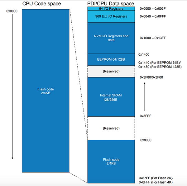
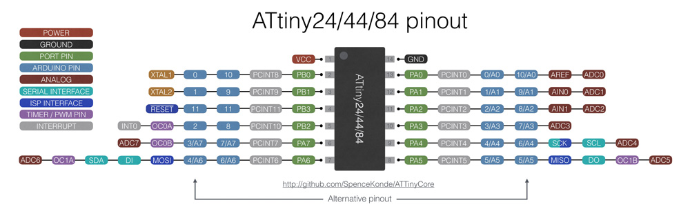
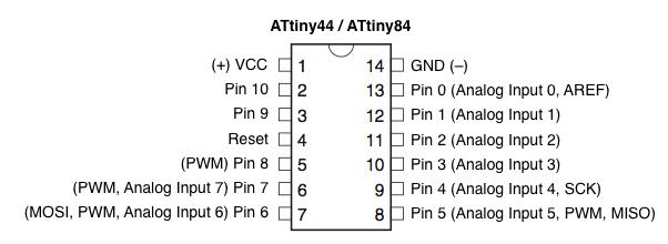
I had written code in arduino IDE and used the Fab ISP to upload the code to my Hello board that has a chip of Attiny 44. So in the fist read the data sheet of Attiny 44 try to understand the function of each pins.
I also read the data sheet of ATTINY 44 that the CMU of my hello board. Here is the map of pin founction of Attiny44.