laser-exposed PCB etching
The general idea is the following: like with other PCB etching processes, we are going to use an acid to etch away the parts of the solid copper surface we do not want to keep. To protect the parts we do want (traces and pads), they need to be covered in paint. Instead of transfering paint from another medium (like with toner transfer), we are going to spraypaint the whole board and then remove the paint in the areas we want to etch using a lasercutter.
Benefits:
- higher resolution than milling
- flatness is not an issue
- files are easy to prepare
Drawbacks:
- requires a lot of consumables
- etchant and residues are hard to dispose of
- can be hard to etch evenly on large boards
- still requires milling for outline, holes
You will need:
- copper-clad PCB stock
- spraypaint
- some solvent to remove the paint
- a PCB etchant (e.g. ferric chloride)
- a small, flat-bottomed container (check for acid compatibility)
- single use gloves (check for acid compatibility)
- a laser cutter
The first step is to clean the PCB stock to make sure it will etch evenly. Without this step, it is likely that some areas on the board are more oxidized than others and will etch slowlier, so that some parts of the board will be either over- or underdeveloped at the end.
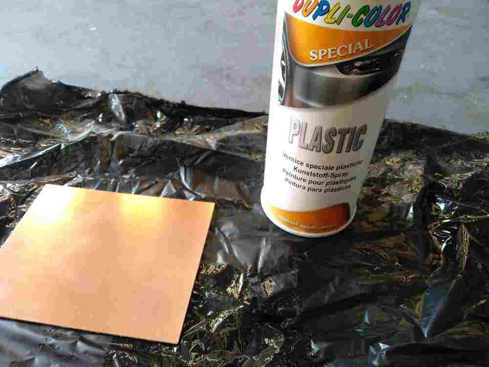
Once the board is clean and the cleaning solvent is removed, the board is coated in a thin layer of spraypaint. It’s best to go with quick, light passes to try and obtain the most even coating possible.
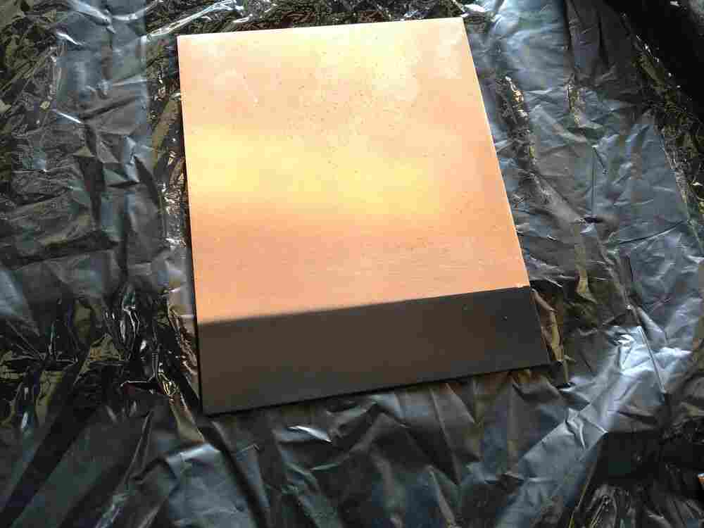
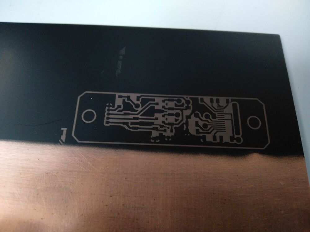
Once the board is fully dried and the (flammable!) solvent has evaporated fully, the board can be put into the lasercutter. Now the paint in the areas that should be etched can be ablated using a raster pass. Try to use the highest resolution your lasercutter supports and try different settings on a scrap piece before attempting a full design. Also make sure to take kerf into account when designing your file.
For our GLS laser, the maximum resolution is 1000dpi and I let it engrave at maximum speed and around 50% power.
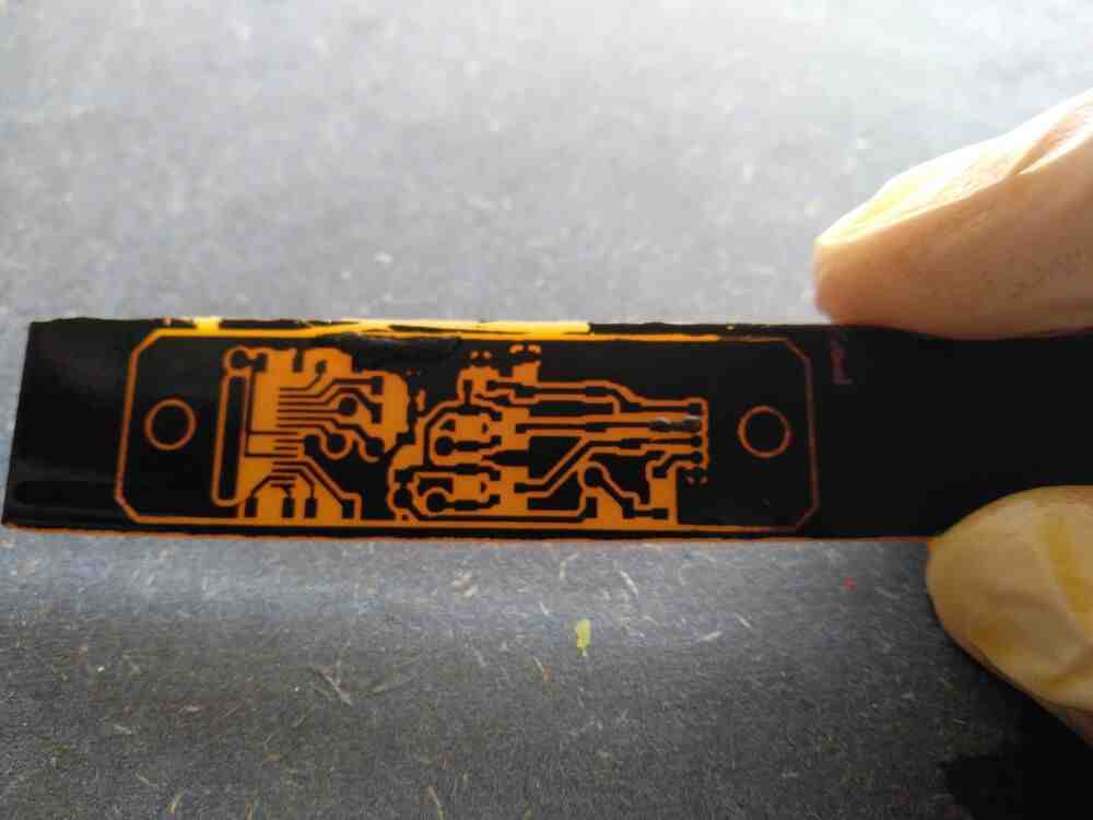
When the laser is done, there is some paint residue left on the board.
I used some regular soap and a paper towel to carefully wipe it off, but I am not sure this step is actually necessary. While cleaning the board, I also broke small details in two places, so I would recommend trying it without or doing this part very carefully.
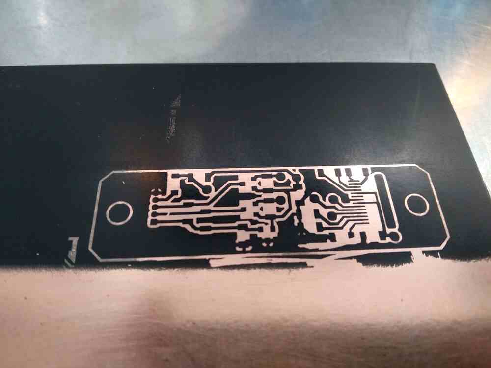
To fix the two parts I broke, I used some rubber putty to cover up the parts where I had scratched off too much paint.
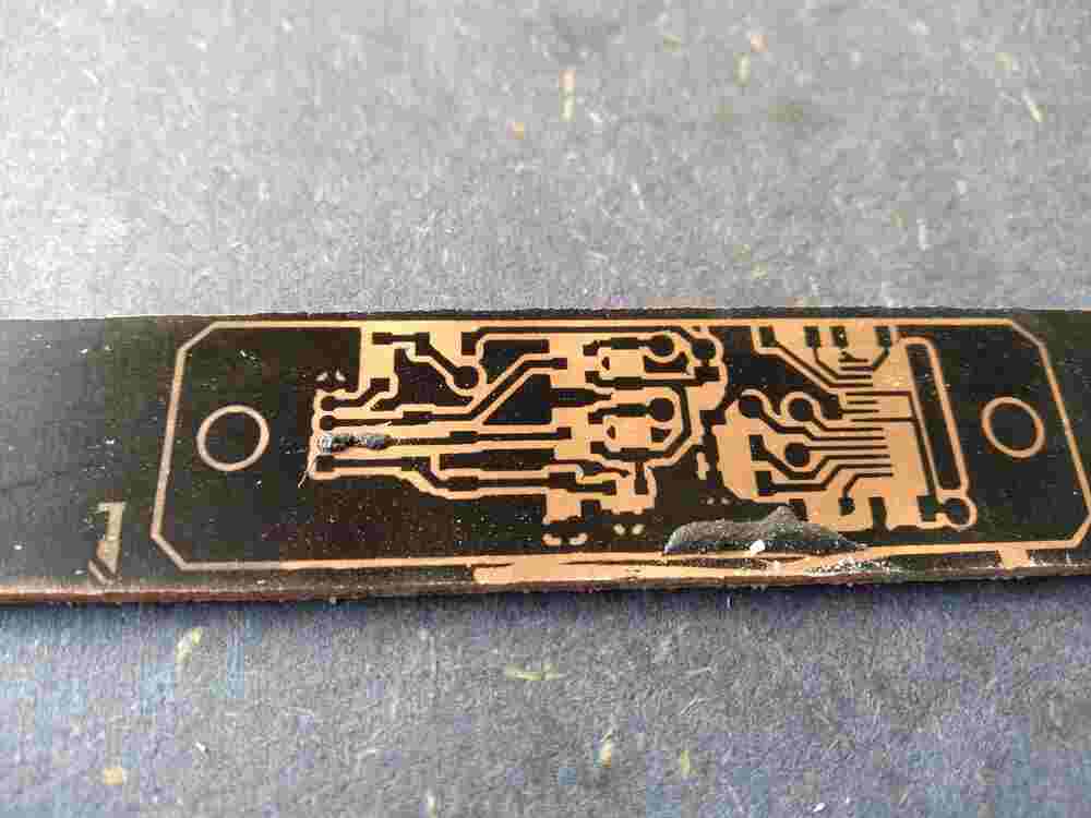
Now the board can go into the etchant. Use as little acid as necessary to fully submerge the top of the board and swirl the container around lightly to keep the acid flowing over the exposed copper evenly to speed up the process.
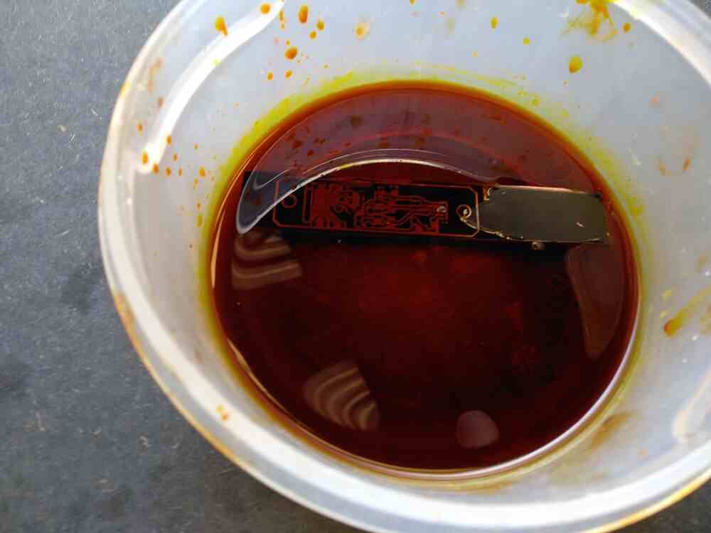
For single-layer boards, the progress can be checked easily by taking the board out and looking at it against a light-source.
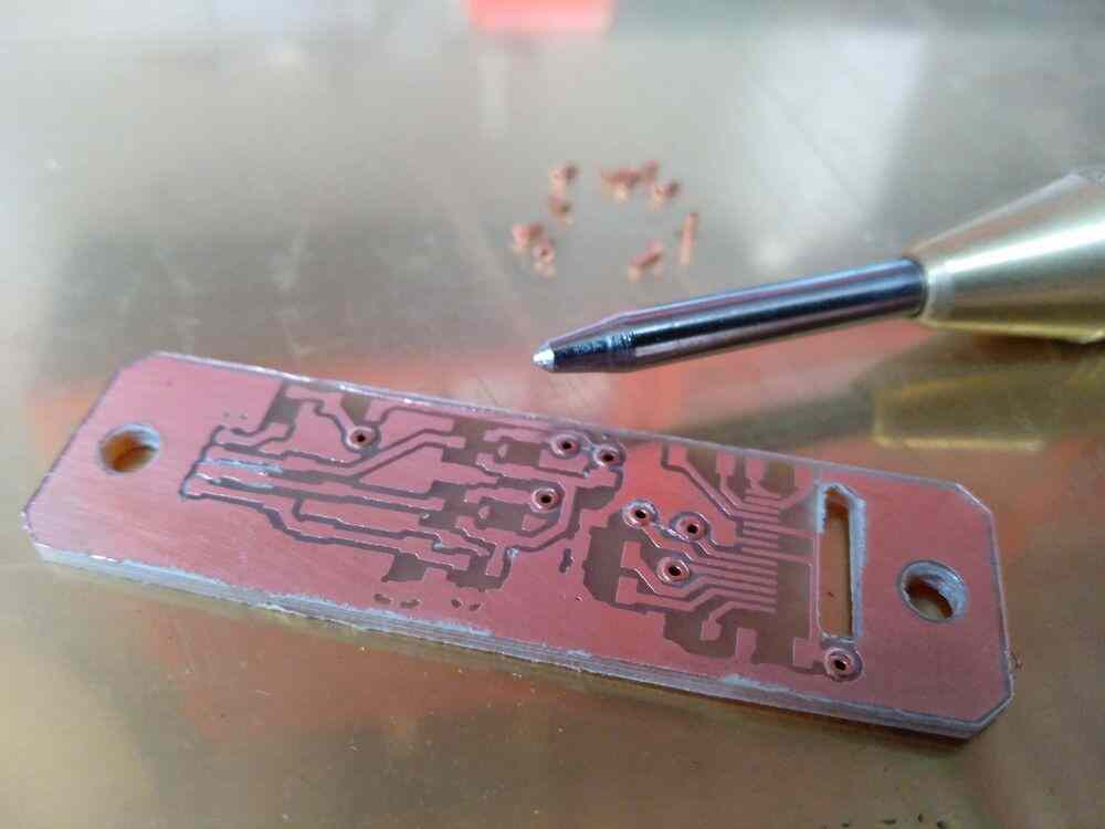
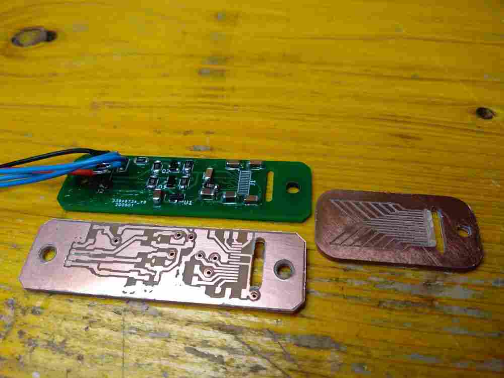
Once the board is done, the acid can be washed off and disposed according to environmental health and safety guidelines. Here is my result:
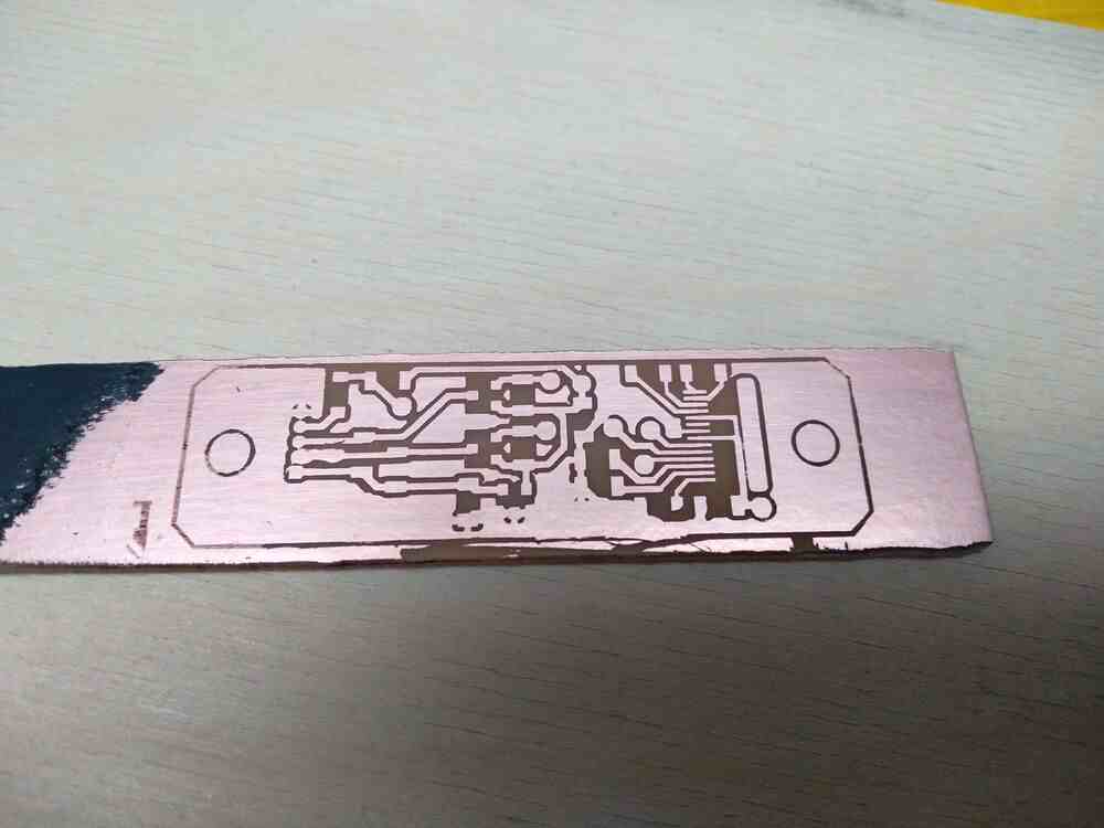
For size reference, the FFC connector on the right has a pitch of 0.6mm and the passives used are 1206 packages.
To drill out the slot and vias I used a CNC mill. I drilled out the two holes that had been marked as part of the etching process by hand and had the mill create two matching holes in the sacrifical layer to screw the board into. This way the board could be aligned rather precisely.
I would however recommend to mark the holes using center marks rather than the hole outline I used to be able to drill them out more accurately.
My design required some vias on the board, so I drilled those holes out as well and used copper PCB rivets to make a connection to the other side.