Week 6- Electronics Design
Overview
For this week we have two assignments:
- Group assignment
- Individual assignment
to use the test equipment in our lab to observe the operation of a microcontroller circuit board. minimum, check operating voltage on the board with multimeter or voltmeter and use oscilloscope to check noise of operating voltage and interpret a data signal.
Redraw one of the echo hello-world boards or something equivalent, add (at least) a button and LED (with current-limiting resistor) or equivalent input and output, check the design rules, make it, test it.
My Assignment Steps:
Step (1):Design The board (Sch- PCB Layout)
Step (2):Milling and solder the board.
Step (3): Test the board and program it.
The Process
Individual Assignments
This week is a complementary work to week 4 where we learned the Electronics Production, Now it is time to make our own PCB :).
Choose your Software
When it comes to electronics design, there is a huge number of software that we can use Eagle, EasyEDA, Kicad.. etc.
As an electronics engineer I'm pretty familier with bunch of them and my recommendation is either to use Eagle or Kicad
Kicad
Kicad is a cross platform open source Electronics Design Automation Suite.it's a little bit complex comparing to Eagle but, it's a full package program in which you are gonna find everything you need. for me it's my no.1 choice.
Eagle
EAGLE is a flexible and expandable EDA schematic capture, PCB layout, autorouter and CAM program. EAGLE is popular among hobbyists because of its freeware license and rich availability of component libraries on the web.
for the Redrawing assignment I' gonna use Eagle but, for my own board I'm gonna use Kicad.
Download Fab-library
Step 1:
you can find a fab-library with all the inventory component Here. download it then create a folder wherever you want the .lbr file to be kept.
Step 2:
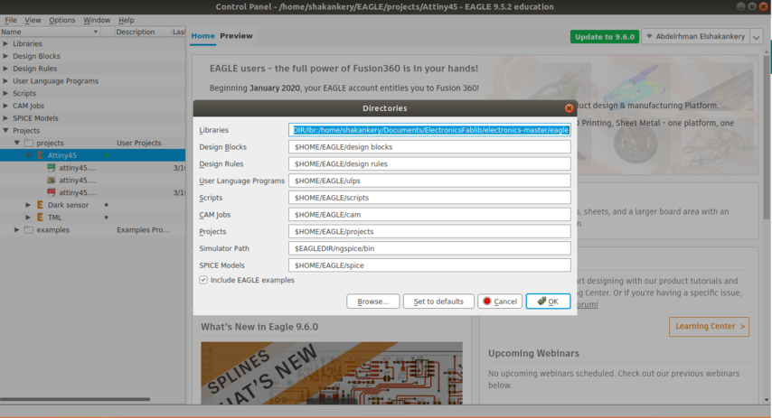
open Eagle form option choose Directories
modify the libraries path location to tell Eagle exactly the folder location and name where it will find the library.
The path must look like -> $EAGLEDIR/lbr:/Users/yourUserName/FileLocation/LibName
Step 3:
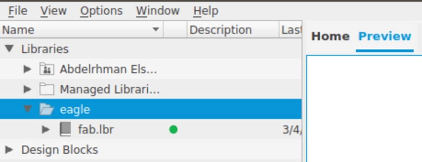
finally from Libraries right click on lib-name andd choose use all.
Board Design
Eagle has two windows that you use simultaneously to design a board:
A schematic in electronics is a drawing representing a circuit. It uses symbols to represent real-world electronic components.
The board layout shows how the electrical components and traces will be laid out on the board.
you need to keep both open all the time as closing one view while the other view is open (and making edits) will break the link between the two
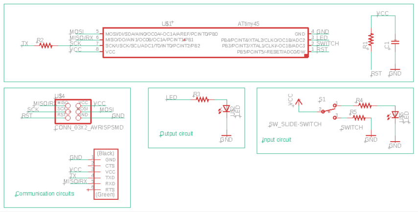
Schematic Design
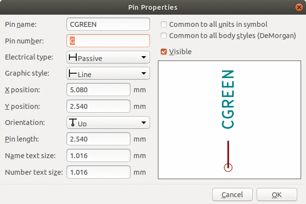
I choose to redraw the Attiny45 circuit and add an indicator LED for power. plus an switch as a sensor to start the main led to blink.
First I add all the component I'm gonna use:
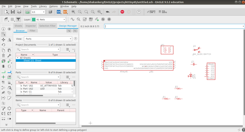
Then it's time to wire the circuit. There are two ways to connect components in a schematic:
I wire my circuit using the second methods.
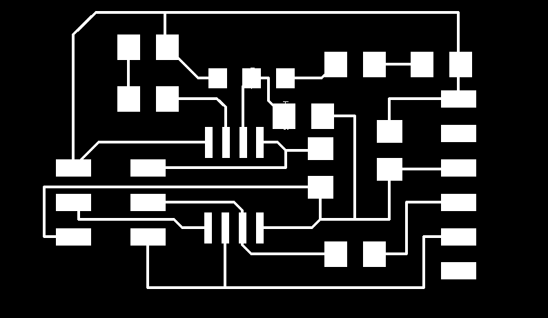
PCB Layout
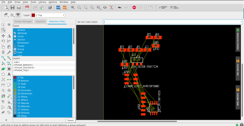
Switch to PCB layout, the components you just added will be jumbled up in a corner with yellow unrouted traces attached.
Start move, organize, route the component as you need.
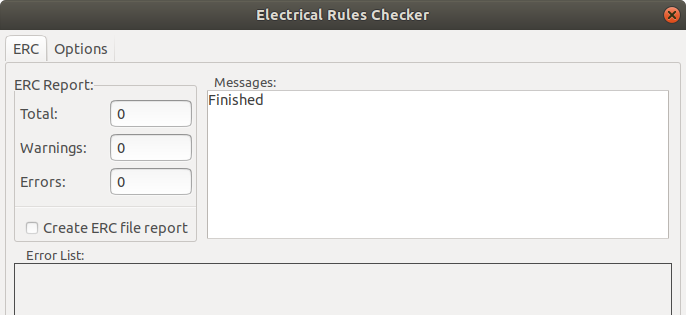
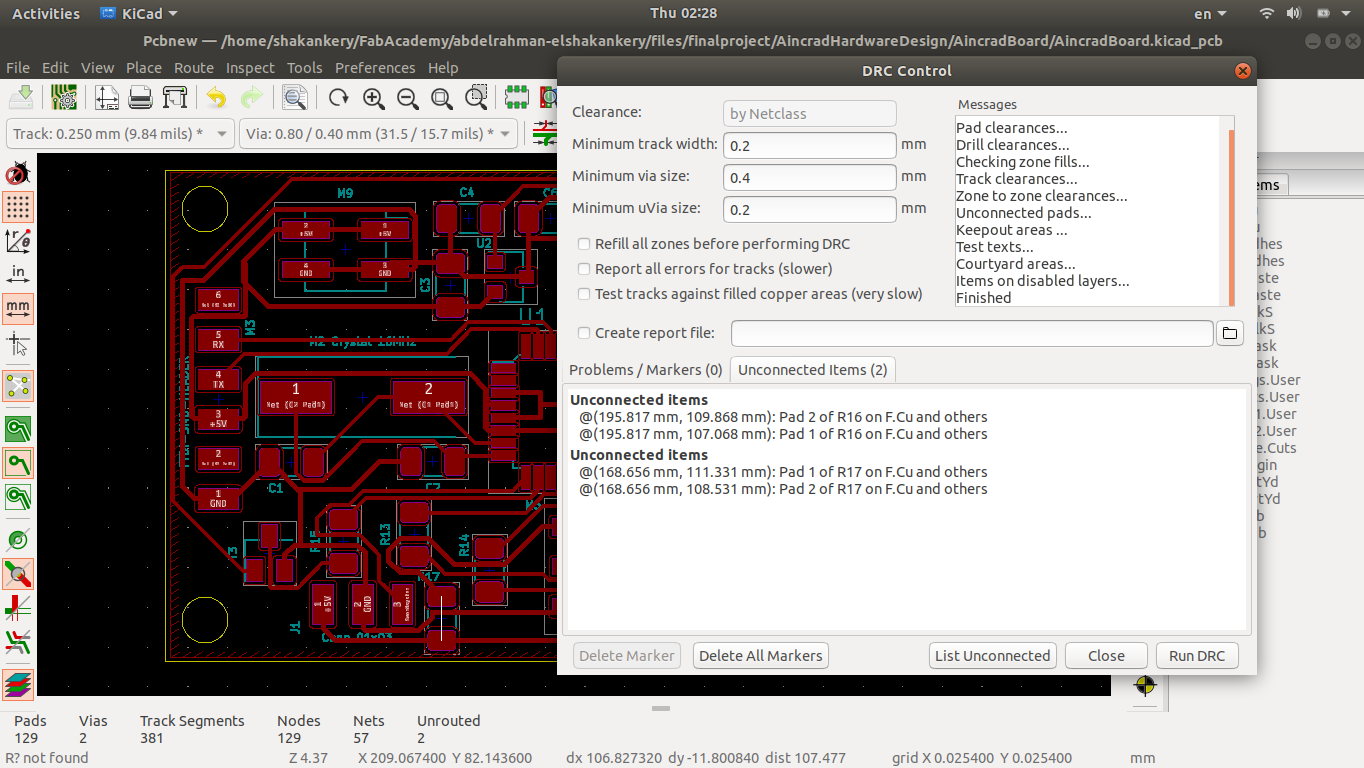
Design Rule check
After designing our board we need to check that the endmill we are using (1/64 usually) is able to go between and around all the traces so the machine is able to cut successfully the board.
a mill-bit with the diameter of 1/64 inch (~16 mil) is used; So I opened the DRC from The "Tools" menu. Then in the "Clearance" tab, I wrote "16mil" to all the fields there.
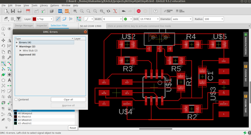
I came up with 4 errors and 2 warnnings. time to fix the circuit :)
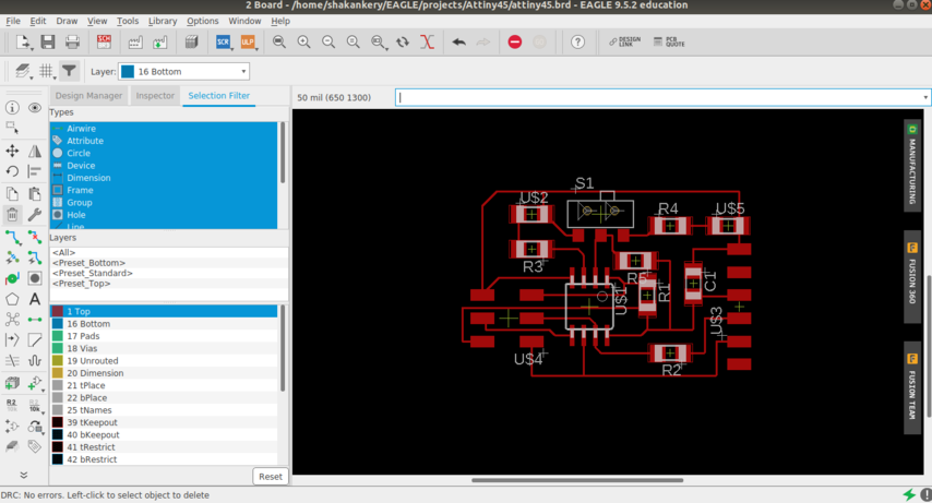
To make sure all is good I run DCR one more time and it came out with no error as you can see in the left corner.
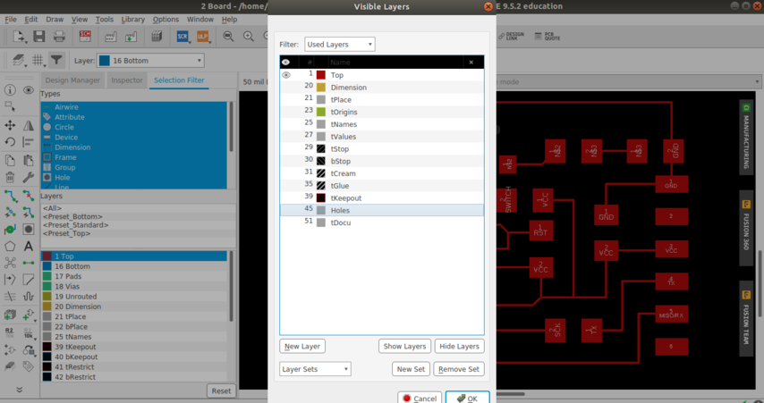
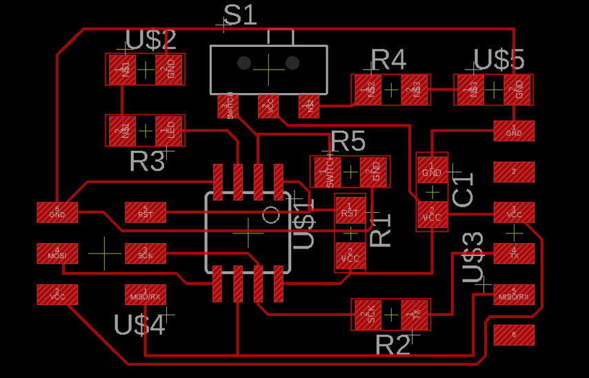
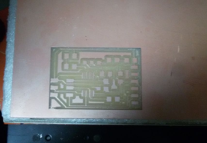
Hide all the layer except for the TOP in order to export the circuit as PNG.
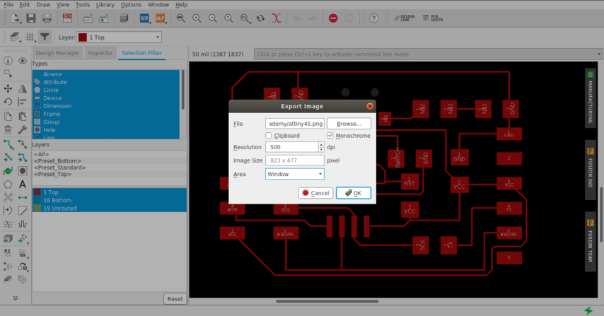
(file -- export -- image),settings should be MONOCHROME and 500 DPI - this will export a image with white traces.
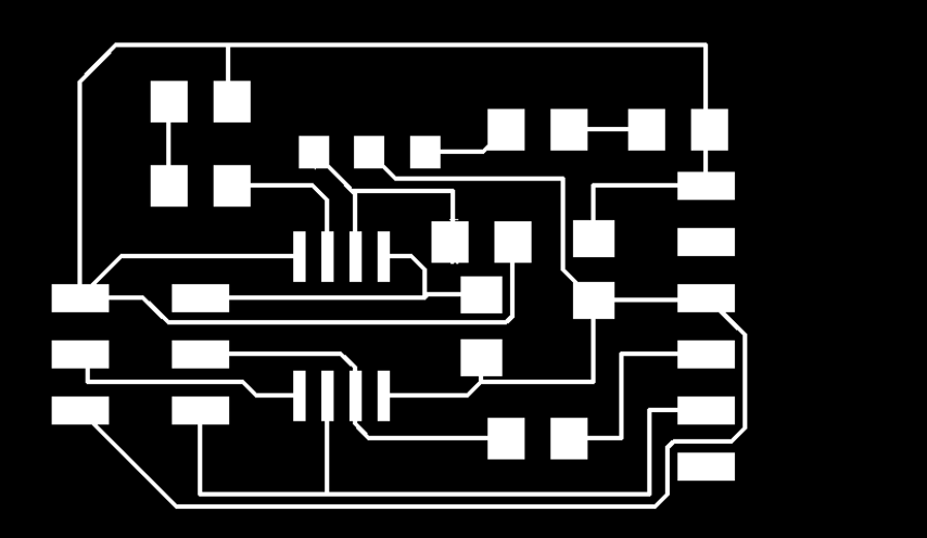
The final output ready to edit in GIMP.
Edit image using GIMP
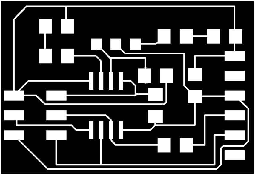
crop the image, add text if you want, from image choose Flatten image and export as PNG.

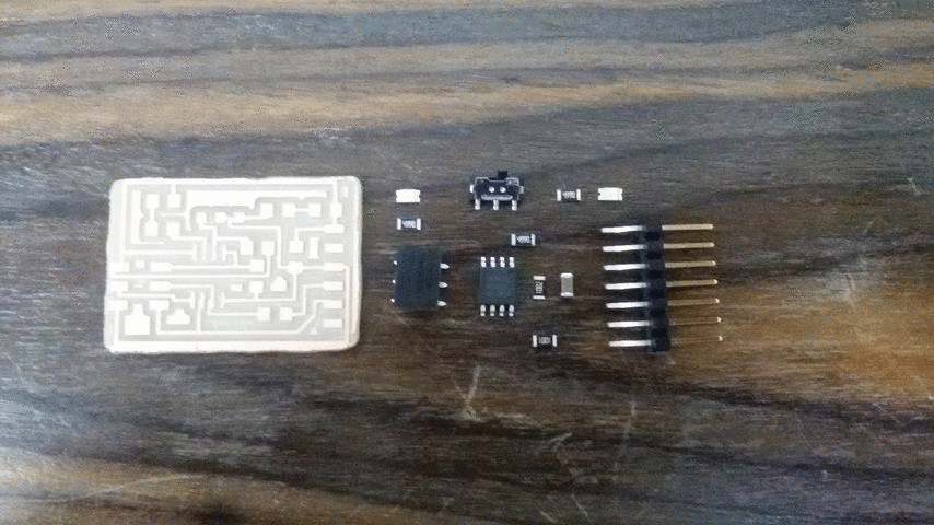
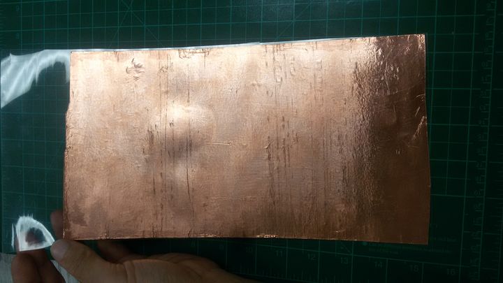
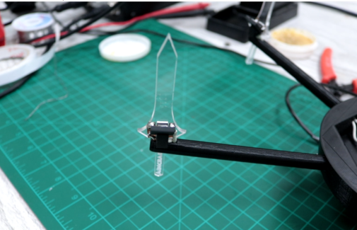
Milling and solder the circuit
following the same steps we did in Electronics production week I was able to solder and mill the circuit.
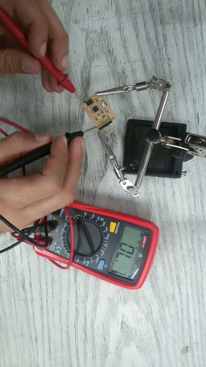
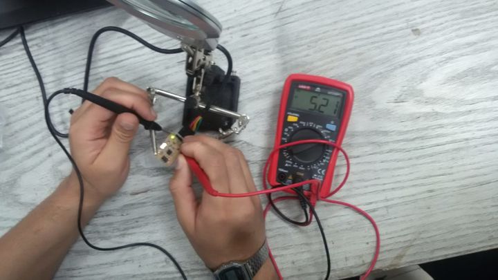
I use the multimeter to verify the continuity of the tracks and to check the operating voltage on the board.
Testing the circuit
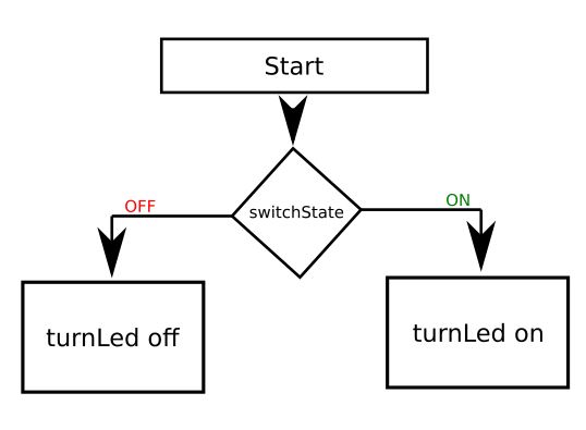
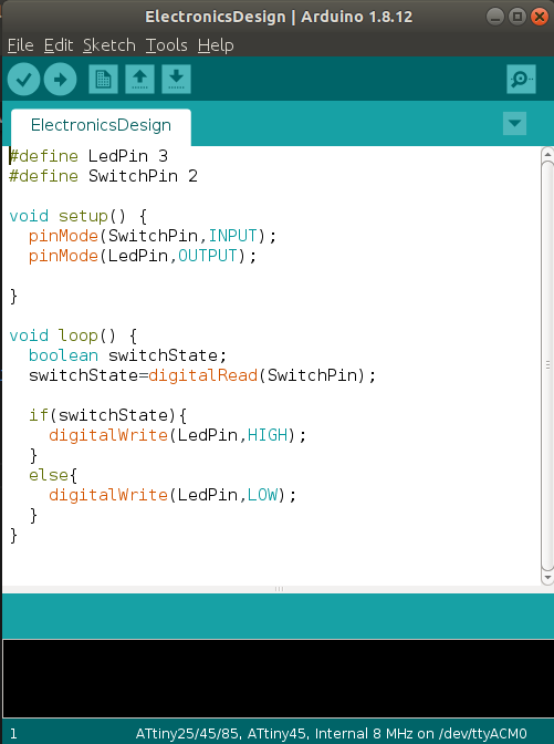
1) The Code:
The idea of the board is really simple we have a switch that work as an input to the Attiny 45 in the case it's high we aria-control any kind if output to be sent to our Led.
for rapid test I choose to write the code in ArduinoC and to use Arduino IDE to upload the code to my board.
#define LedPin 3
#define SwitchPin 2

void setup() {
  pinMode(SwitchPin,INPUT);
  pinMode(LedPin,OUTPUT);

}

void loop() {
  boolean switchState;
  switchState=digitalRead(SwitchPin);

  if(switchState){
    digitalWrite(LedPin,HIGH);
  }
  else{
    digitalWrite(LedPin,LOW);
  }
}
2) Program The board
Time to focuse now !!
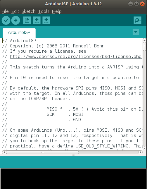
we will going to upload the code to our board using arduino IDE and using arduino as our programmer as we did in Electronics production week
1- Install Attiny library support for Arduino IDE
https://raw.githubusercontent.com/damellis/attiny/ide-1.6.x-boards-manager/package_damellis_attiny_index.json
2- Prepare the arduino Board as a programmer
3- Upload the Bootloader
slave reset: 10
MOSI:        11
MISO:        12
SCK:         13
4- Upload the Code
Final Project
Well first spiral it's all about hardware design and embedded programming by the end of it I should be able to :
so without further ado let's jump to the steps.
ELECTRONIC CIRCUITS (PCB) DESIGN AND FABRICATION
I need to design 3 board for Aincrad:
- The Master board that control the sound sensor and the lighting system
- Sword lighting board 5 total.
- Sword lighting - Master interface board.
1) Aincrad Master Board:
Specifications (Electrical)
- Output drive capacity = 5V.
- Input signal from any sound sensor and ""bluetooth in future""
- Output signal to lighting system consist of 3 RGB led/castle body and 5 Led for each sword.
- PWM channels to control the lighting system and the "motor in future"
- Assume in all power calculation that copper layer is only “1 oz thickness”
Depend on this specification I could use either 2 Attiny-family board one for the input and the other for the output and let them communicate with each other through serial bus. or an atmega-family board with all in on system.
I go for the second option in order to save space and for more neatness in the final connections.
Specifications (Mechanical)
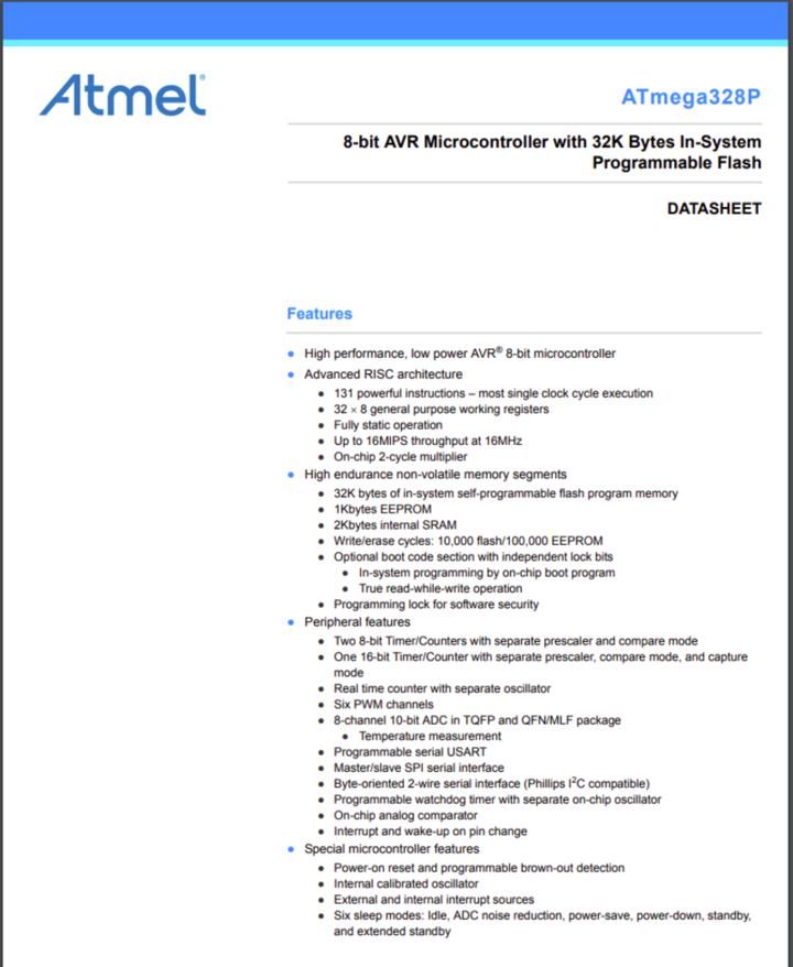
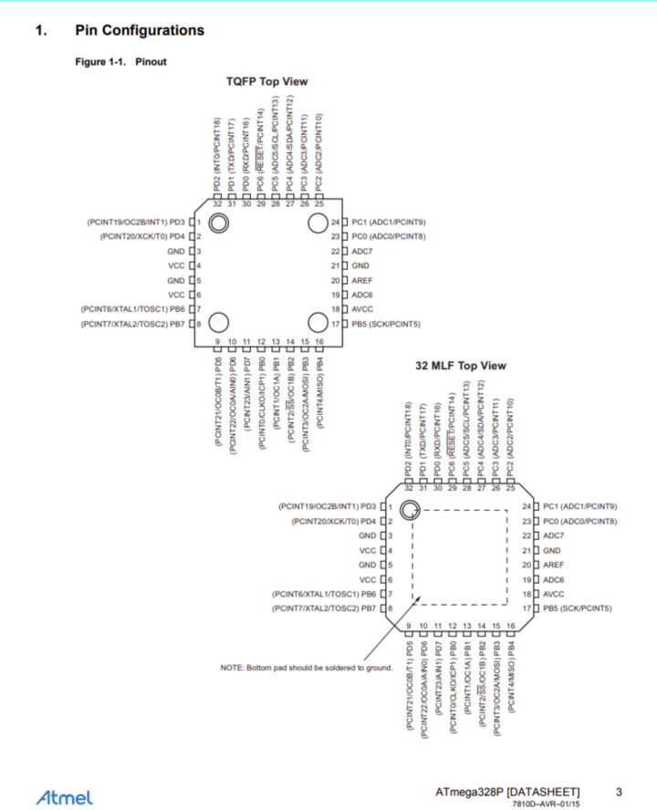
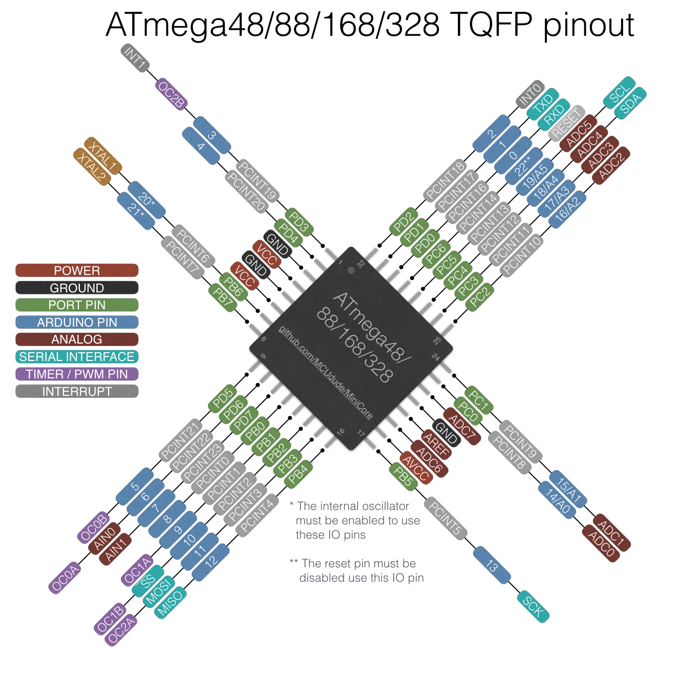
- Use 32-pin TQFP For Atmega328p-au know more about it from datasheet
- Board dimensions with curved angels
2) Block Design

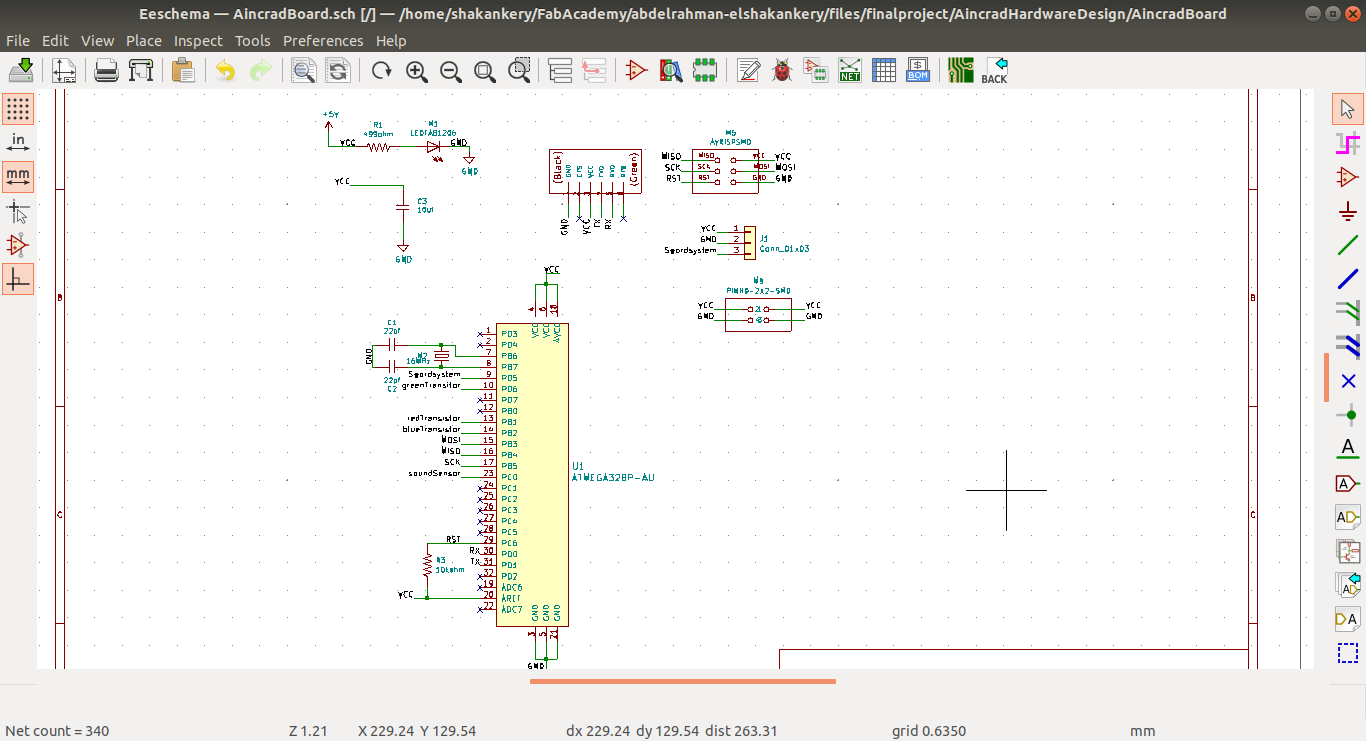
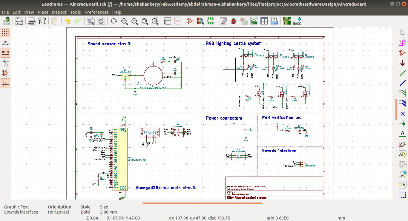
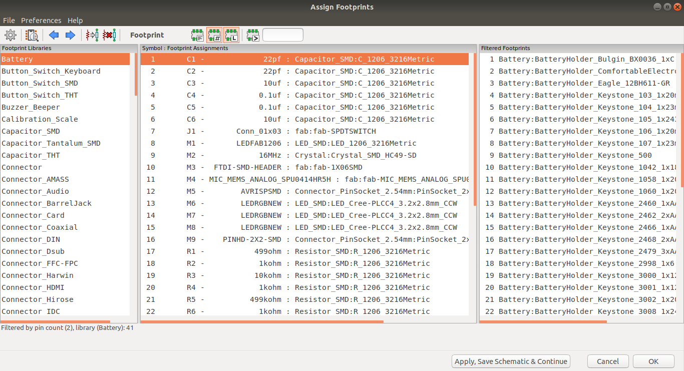
3) Schematic Design using Kicad
I divided the master board into 3 main functioning citcuits
- Atmega328p-au circuit + interface
- Sound sensor circuit
- Castle RGB lighting circuit
Atmega328p-au circuit + interface
your number one friend through this step is the datasheet. So from the Atmega328 datasheet I was able to
know:
Atmega328p-au specifications
Circuit Components
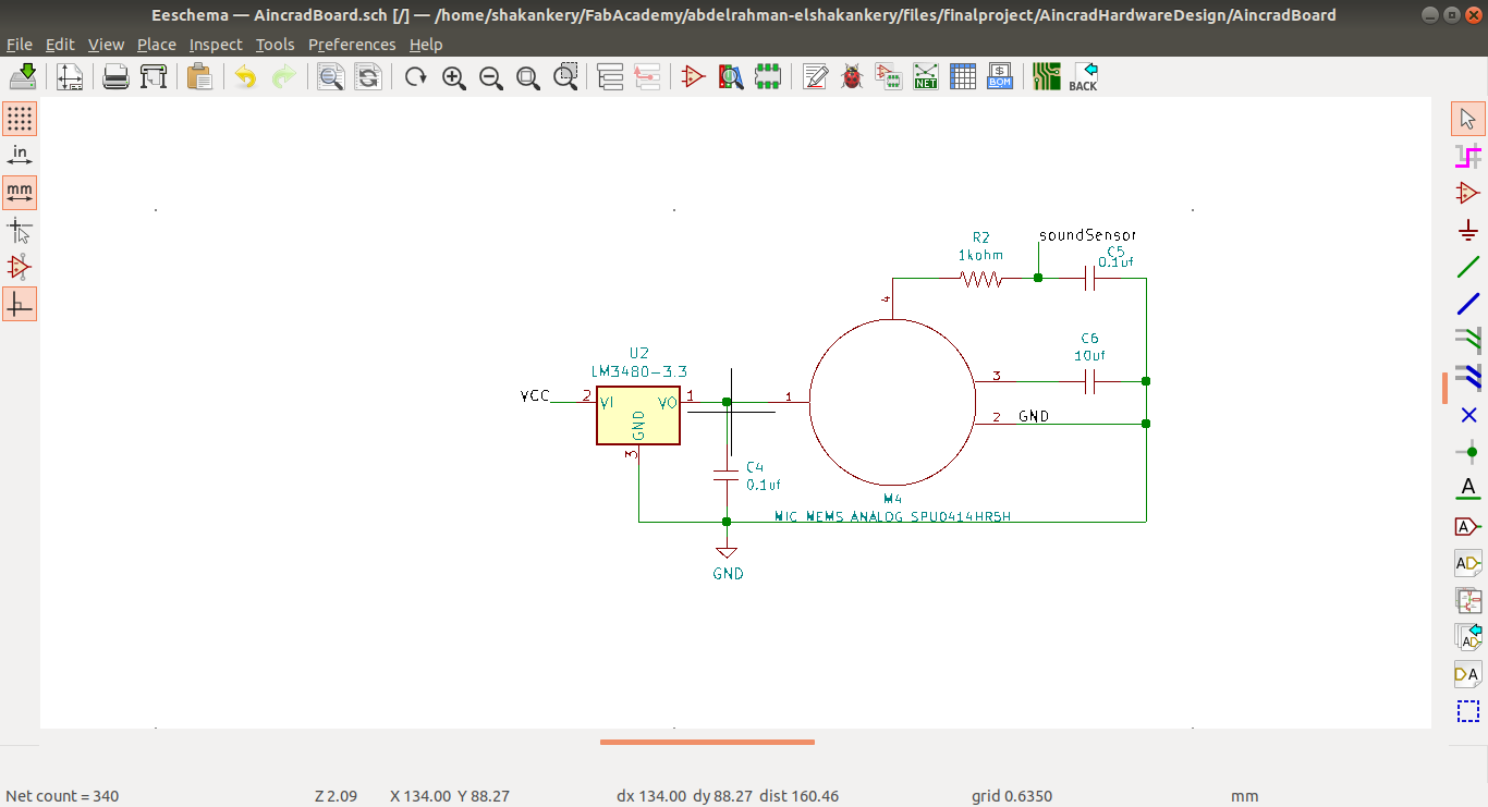
Sound sensor circuit
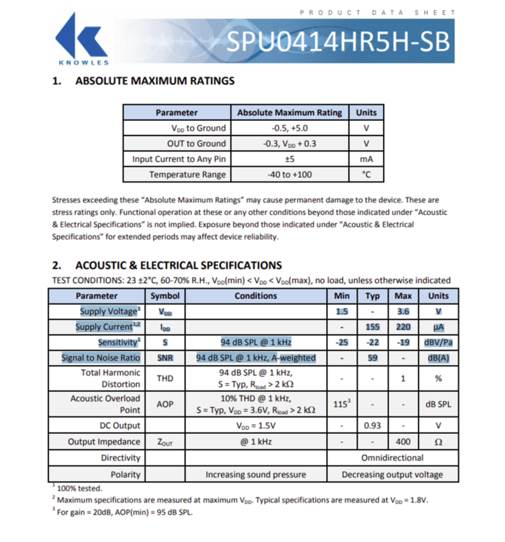
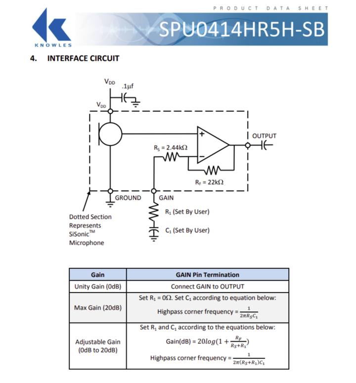
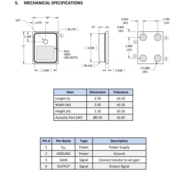
SPU0414HR5H-SB MIC for sound sensor specifications
- Up to 20dB of Gain
- Maximum supply voltage 3.6V
- Maximum Low Current 220uA
- Signal to Noise Ratio SNR 94 dB SPL @ 1 kHz, A-weighted
- RECOMMENDED REFLOW PROFILE Peak Temperature (TP) 260°C
This specification means I will need to use a voltage regulator with the sensor in order to convert the 5V power to 3.5V
Circuit Components
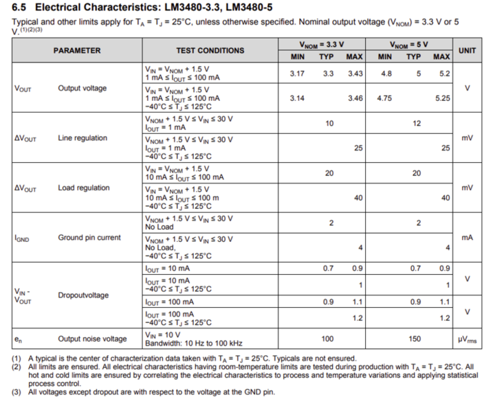
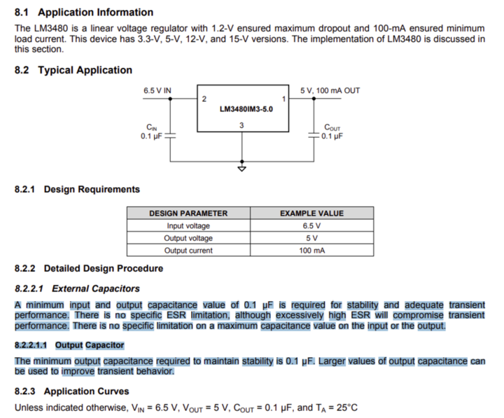
So now in order to design the circuit I need to choose a voltage regulator to convert 5V power to 3.5V I go with LM3480 Low-Dropout Linear Voltage Regulator
LM3480 Linear Voltage Regulator specifications
from the datasheet
- Input Voltage Range: up to 30 V
- 3.3-V, 5-V, 12-V, and 15-V Versions Available
- 100-mA Ensured Minimum Load Current
- SOT-23 Package
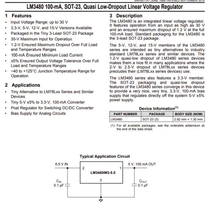
Vout= 4.8-1.5= 3.3V
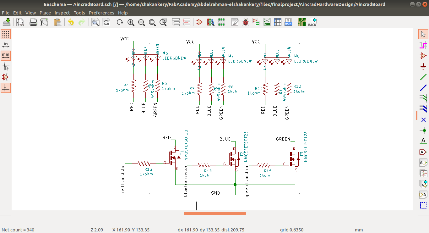
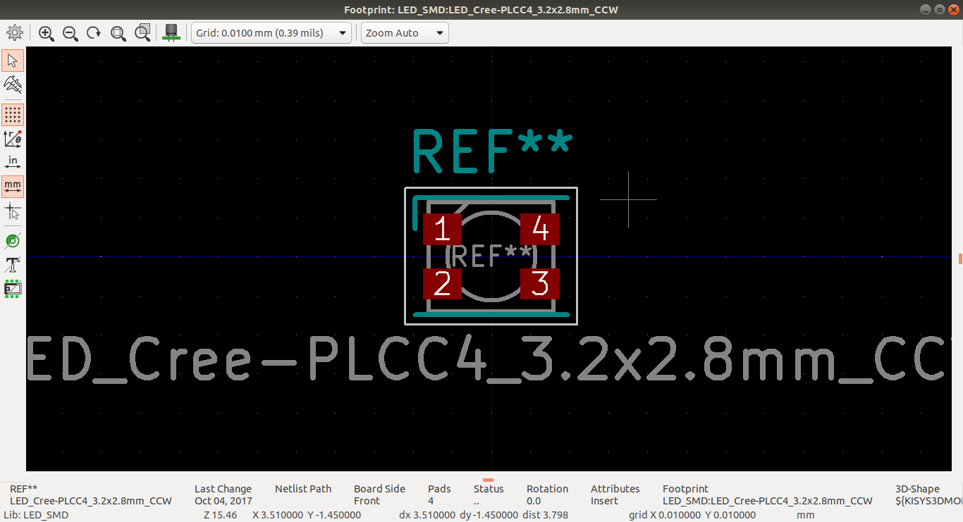
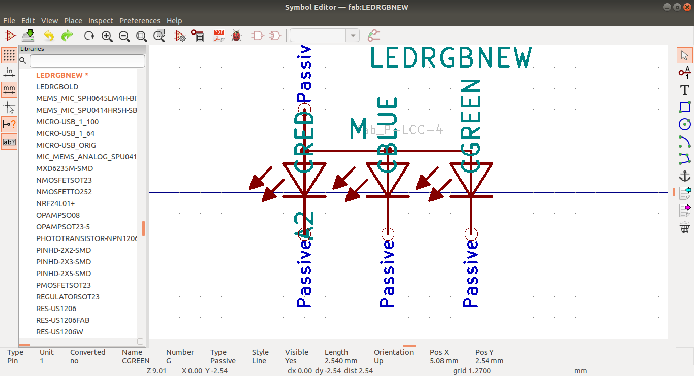
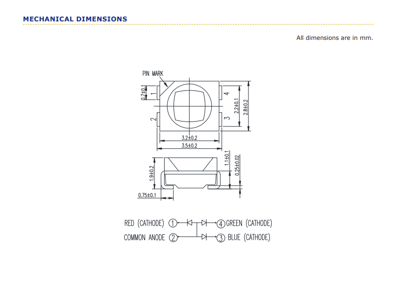
Castle RGB lighting circuit
Cree PLCC4 3 in 1 SMD LED specifications
from RGB LED datasheet
- Size (mm):3.2 x 2.8
-
Dominant Wavelength:
- Red (619 - 624nm)
- Green (520 - 535nm)
- Blue (460 - 475nm)
-
Current= 20mA/Led when
- Red (2V)
- Green (3.2V)
- Blue (3.2V)
Circuit Components
However I would like to add 2 more LED's to my project, but I don't want to take up every single
PWM. So I'm going to use n-channel transistors and duplicate per color channel pin
At 20mA per led, 3 per channel, that's only 60mA. so make sure your power supply can support
that.
60 * 3, that's 180mA on the leds alone, not including the rest of the board.
Then for the master board:
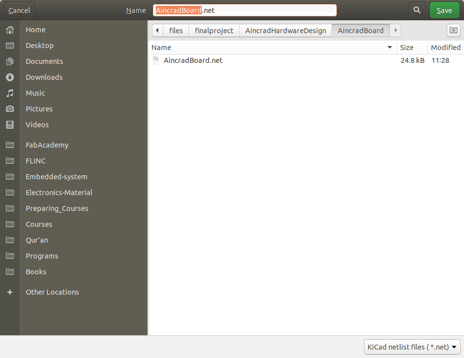
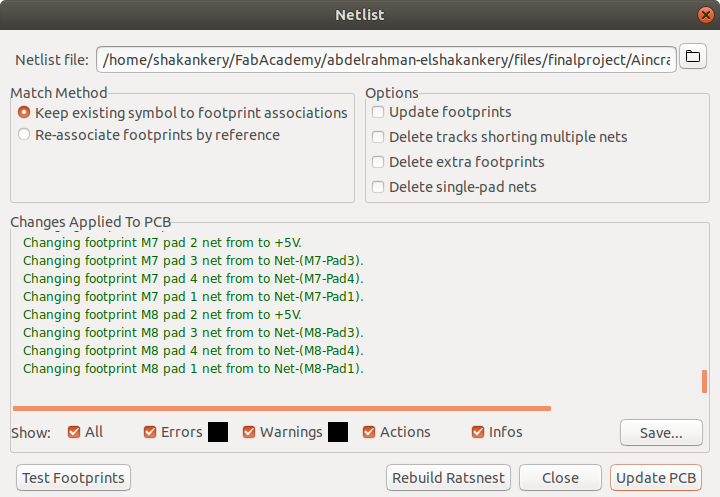
Generate the Netlsit is the final step after finishing all the design. This step is really important in order to connect the schematic with PCBnew in which we will going to create the PCB layout. Now it's time for the layout design.
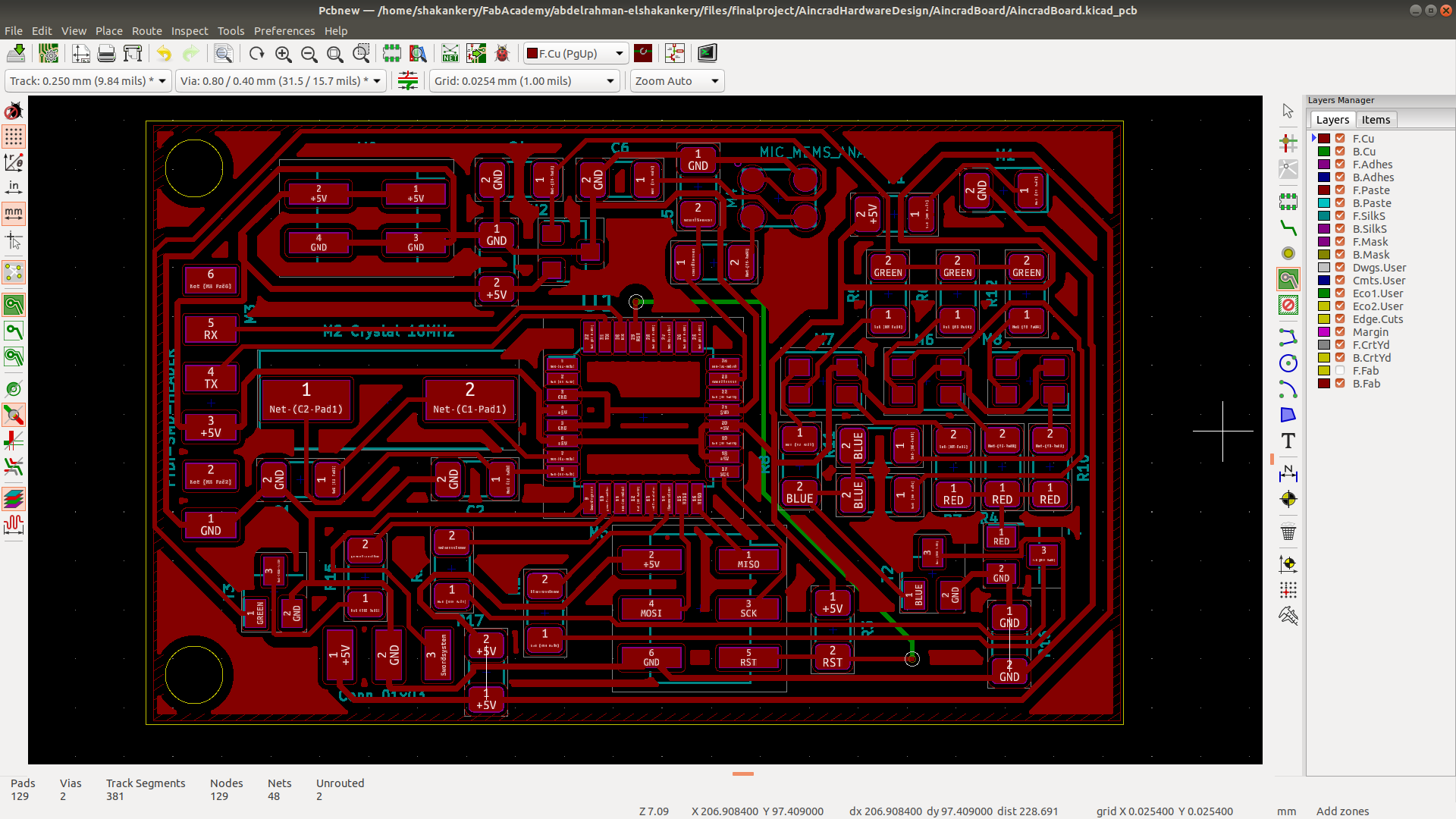
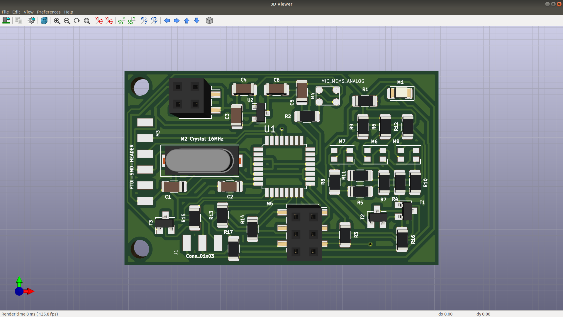
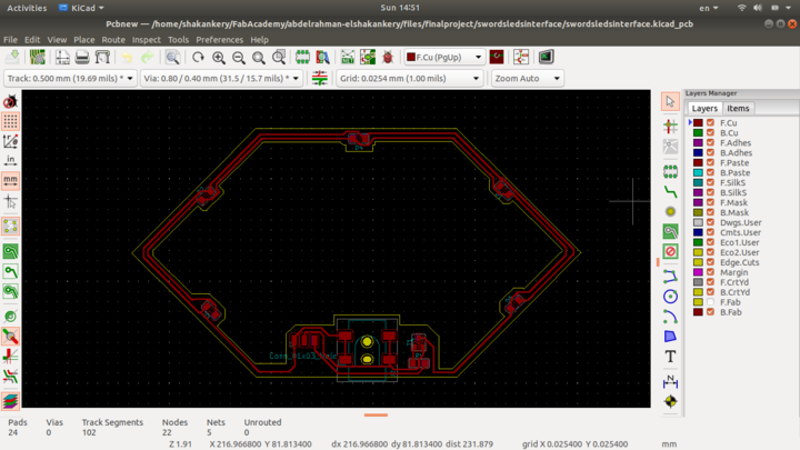
4)PCB layout
Challenge time
As soon as I start reading the Netlist I got an error message about the rgb-led Pads. at first I
didn't understand it's meaning then I found the issue once I move the rgb-led away It's not
connected to any other component of the circuit.
So in this section I will walk you through the steps in which I was able to solve this Challenge
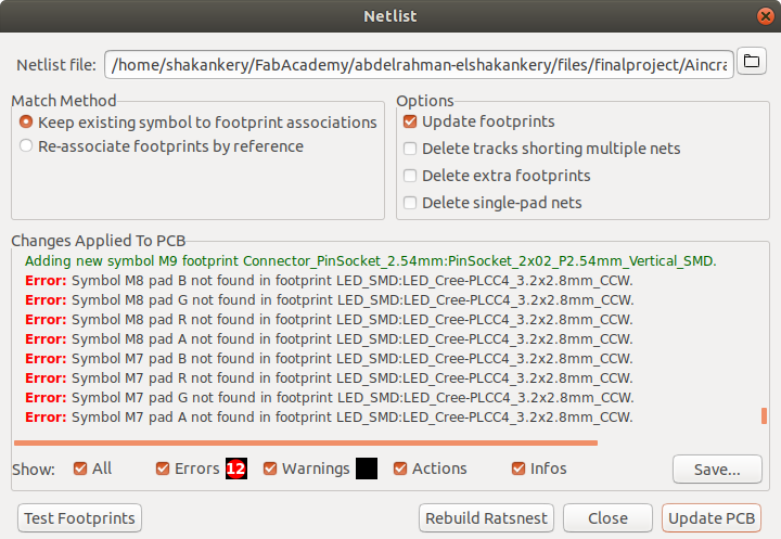
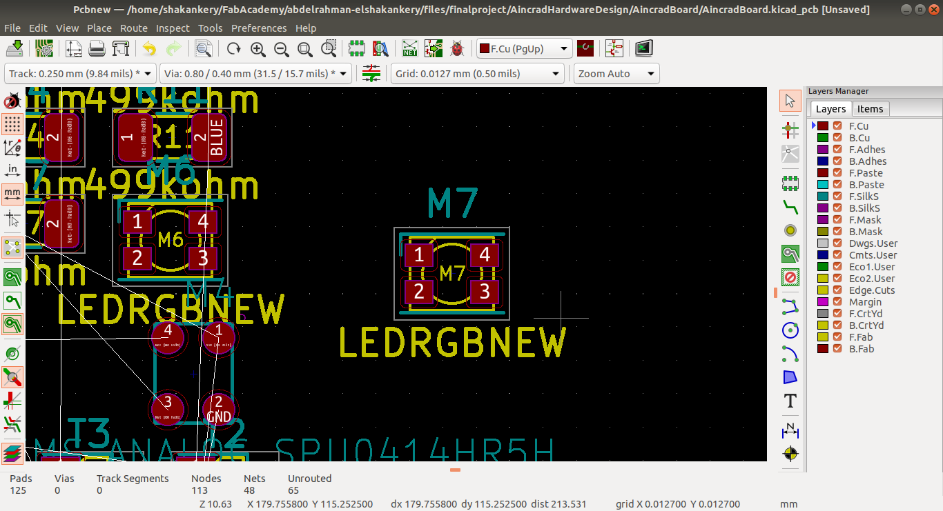
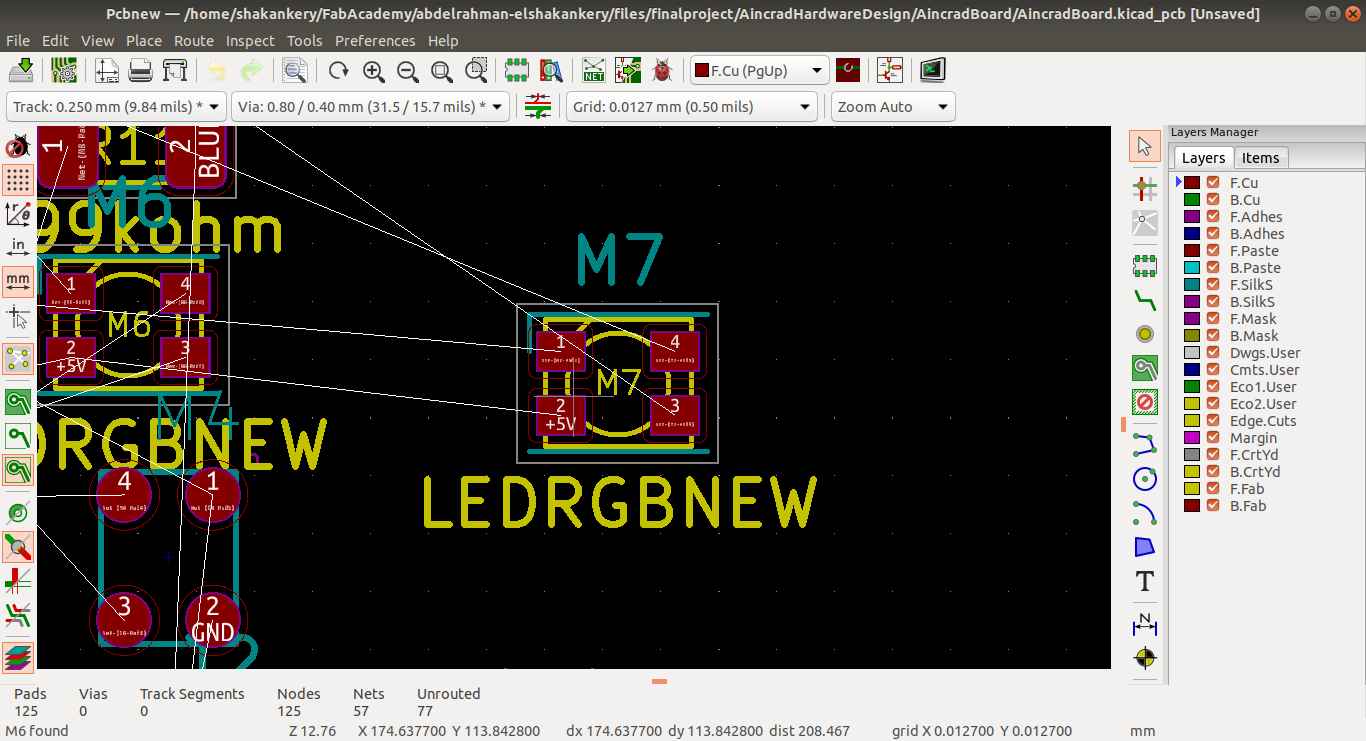
Following the same process we did in electronics design weeks and After 12 hr of routing and component placment adjustment I was able to finish all the board in 1.5 layer + RST pin.
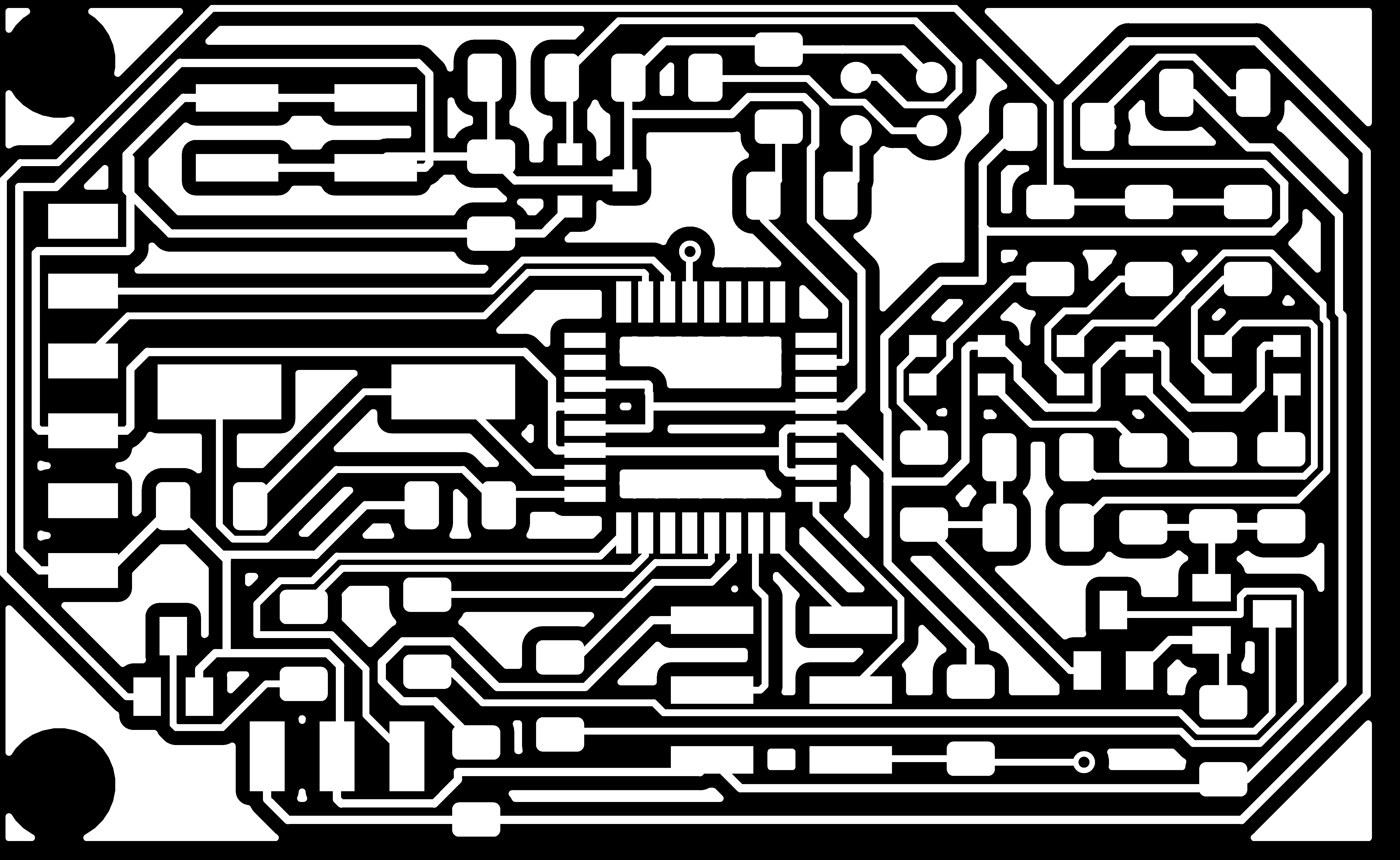
Export .svg file from kicad for the board and Edgecut layer then run our Automatic conversion using imagemagick to get the .png files ready to be used in mods.

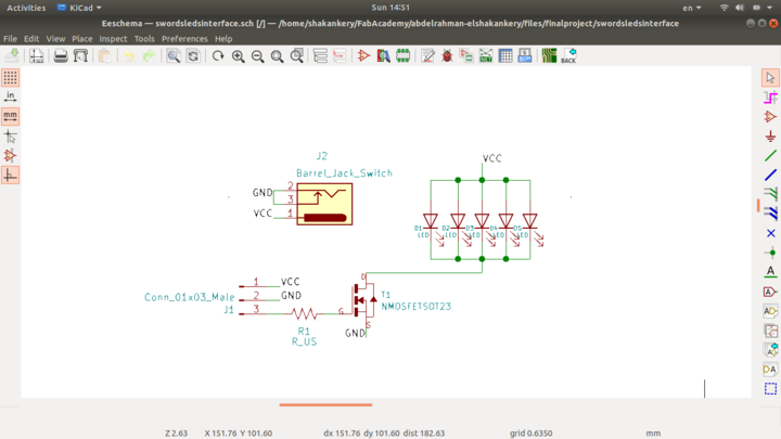
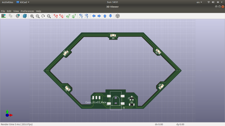
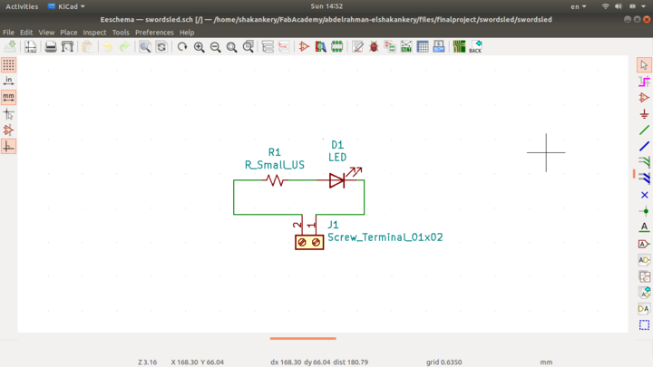
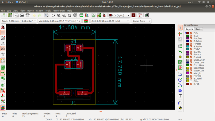
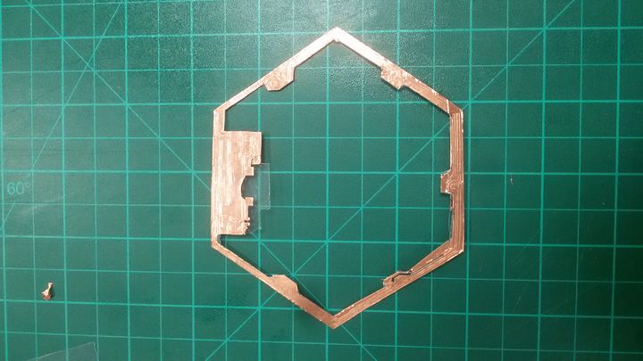
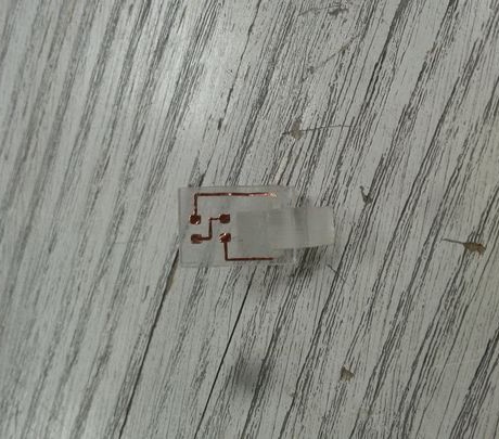
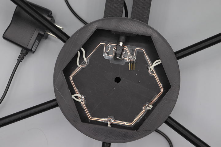
Integration hexagon and led sword interface boards
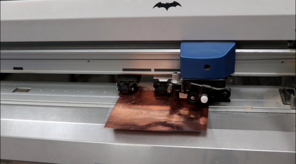
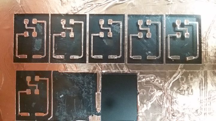
following the same process I have created 2 boards using Kicad and implement them using the vinyl cutter following this AMAZIGN TUTORIAL
-
led sword interface circuit.
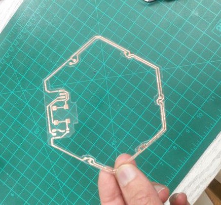
- integration hexagon circuit.
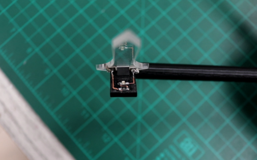 system assemply (1).
 system assemply (2).
 system assemply (3).