Electronics Design
Week06
Electronics design refers to understanding the process of creating a pcb from scratch. This process usually starts with the requirements to the board by the intended application. As an example, we use a standard board with an ATmega88 microcontroller that may be used for a variety of different applications. The ATmega88 microcontroller (pinout from data sheet see Fig.01) forms the centerpiece of the board to be designed in Eagle. There, the design starts with opening a new project in schematic view, then importing the relevant libraries: FAB_Hello and fab (Fig.02).
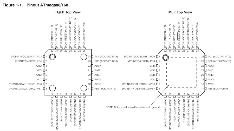 Fig.01: Pinout ATmega88, retrieved from data sheet. |
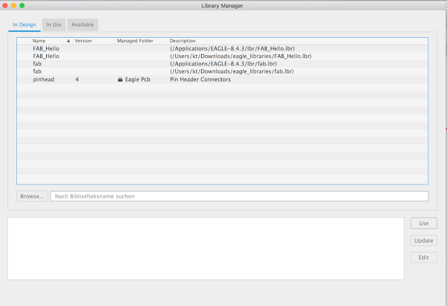 Fig.02: Eagle library manager. |
Apart from the ATmega88, the assignment required the exposure of as many of the ATmega's pinouts as possible (or useful) - plus the regular connectors to the power source (5V/VCC and ground/GND), the programmable pinouts (MOSI/MISO), the pinouts to the interruptors, and adding a reset button and a LED to the board.
The design starts in Autodesk Eagle with the schematic view (Fig.03), into which the board components are imported from abovementioned libraries. Being specific about those components is rather important, since they come with exact properties including dimensions - which is one of the key factors for the subsequent design in Eagle's board view. In schematic, the board's components are only to be arranged logically, the exact position does not matter here. In fact, the position matters so little in this view, that connections between two components may simply be indicated by a label (Fig.04); the arrangement of the traces is left for the next step in board view.
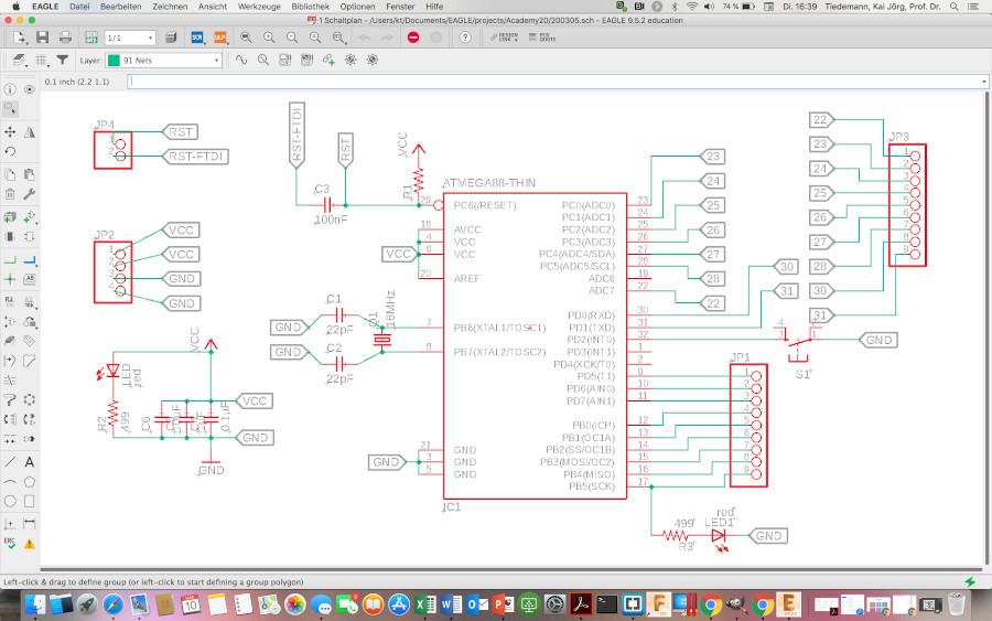 Fig.03: Eagle schematic view for logical arrangement of components. |
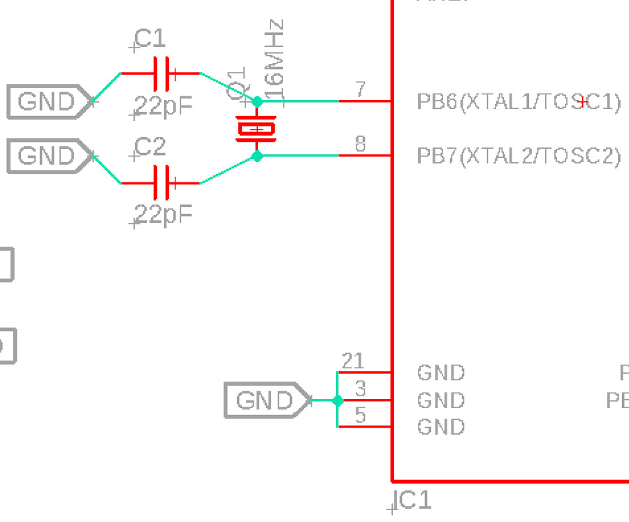 Fig.04: Cutout from previous with labels indicating trace connections. |
After all the components are added to the schematic view and properly connected, we switch to the board view, where initially all those components are placed somewhere in the lower left corner. The layouting process typically begins by placing the largest part, our ATmega88 microcontroller. Once the ATmega was placed, the remaining parts follow. Some general rules should be considered, though:
- the board should be designed efficiently, i.e. in order to minimize the use of material;
- functional units should be placed in immediate proximity;
- the capacitors in general should be placed as closely to the microcontroller as possible;
- the capacitors to the crystal should be placed in close proximity to the crystal.
This is a trial-and-error puzzle process that (according to our instructors) becomes easier with experience. For a first-timer, though, it takes a while for the pieces to fit out little puzzle. Eventually, eveything seems to fall into place (Fig.05).Before proceeding to the generation of the gcode for the milling process, Eagle can check the configuration using the command tools > test layout (DRC) (Fig.06). This is a quite useful function, for it reveals Air Wires, i.e. unconnected and/or illogical traces. In my case, it discovered various air wires due to
- isolated GND "islands" that had formed, disconnected from the ground plate, and
- missing connections due to an error in the schematic view, where I copied labels instead of placing a new one; for a copied label, Eagle does not ask where to connect them.
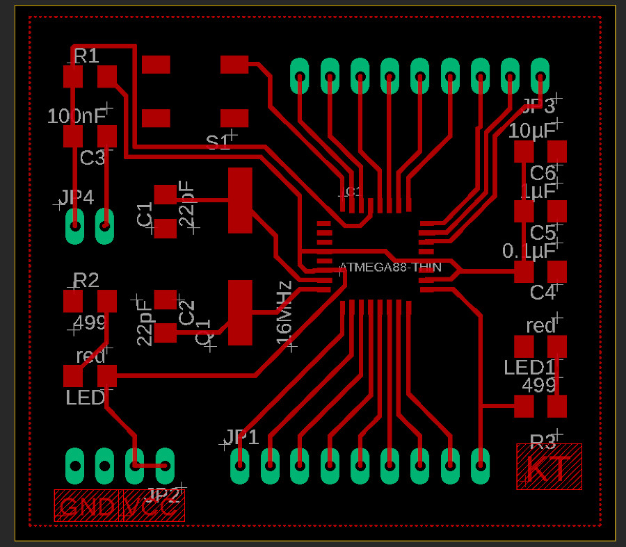 Fig.05: Eagle board view after arrangement of components. |
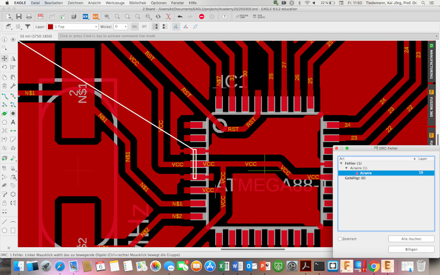 Fig.06: Air wire indication as result of layout test. |
After the board view is confirmed to be error free, it must be converted into black&white pictures in preparation of the gcode generation with FabModules. Using GIMP2.10 I produced three bw pictures in .png format: one pic for the traces (Fig.07), one for the outline (Fig.08), and one for the holes that will hold the pin headers (Fig.09). It is important to choose a high resolution for those images (between 1000 and 1500 dpi; I chose the latter) to make sure that the milling process finds an adequate resolution for high-end precision milling. Due to an uneven copper board, the milling did not produce a satisfiyng result neither after the first nor after the second run with an adjusted (deeper) z-home. Hence, I produced a forth pic, a cropped version of the traces where only the insufficiently milled parts of the board appear (Fig.10).
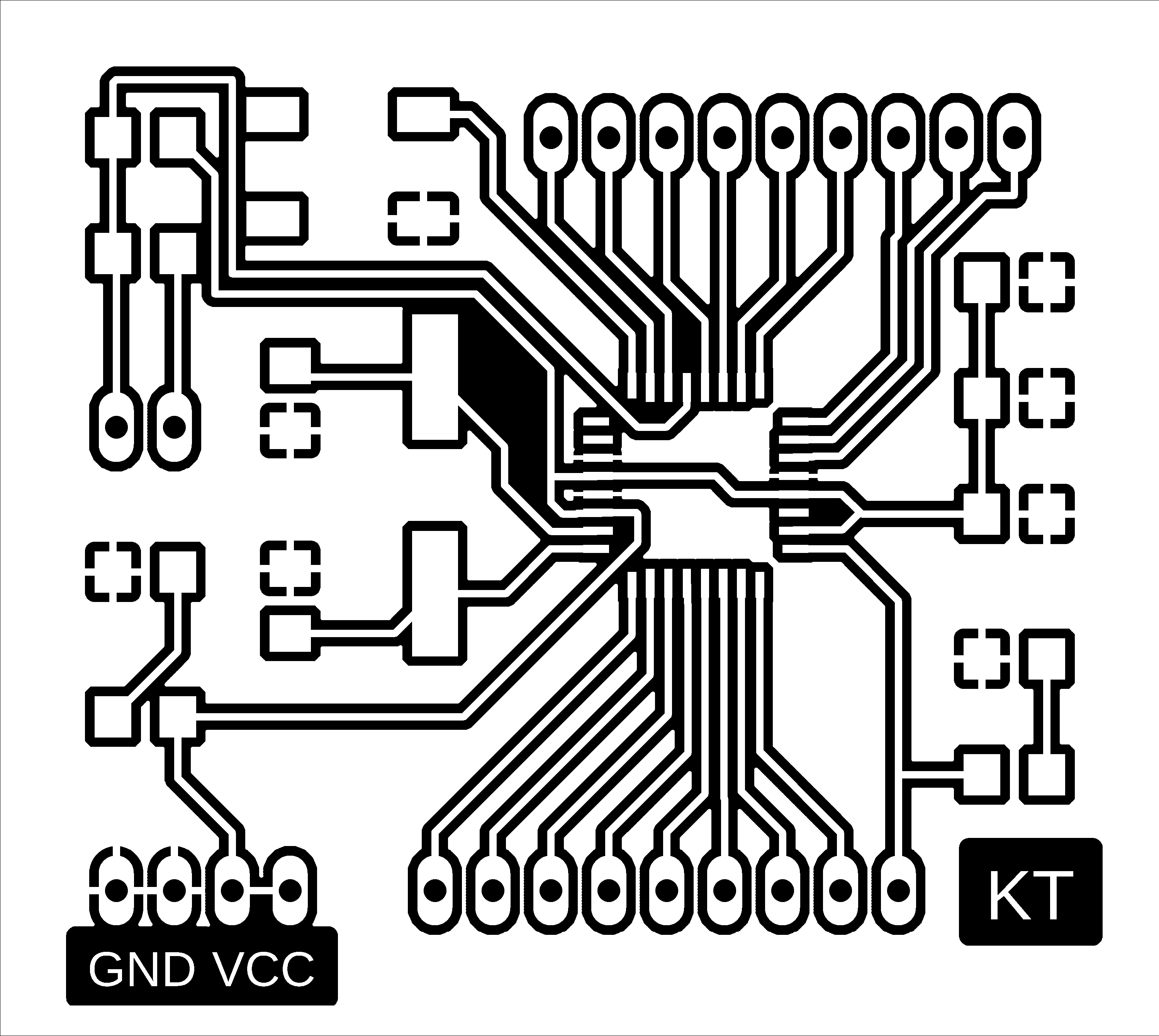 Fig.07: BW .png image of traces. |
 Fig.08: BW .png image of outline. |
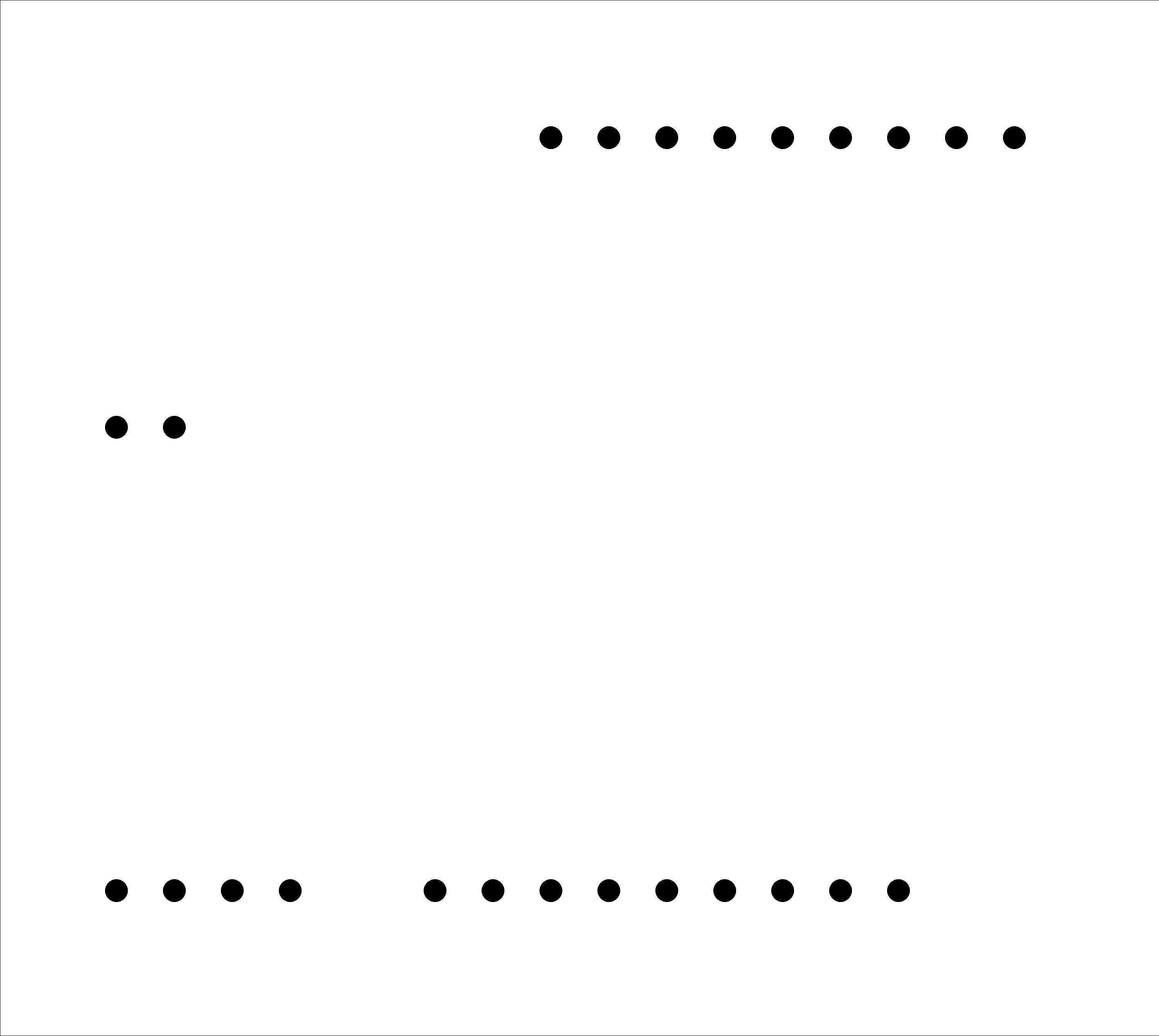 Fig.09: BW .png image of holes. |
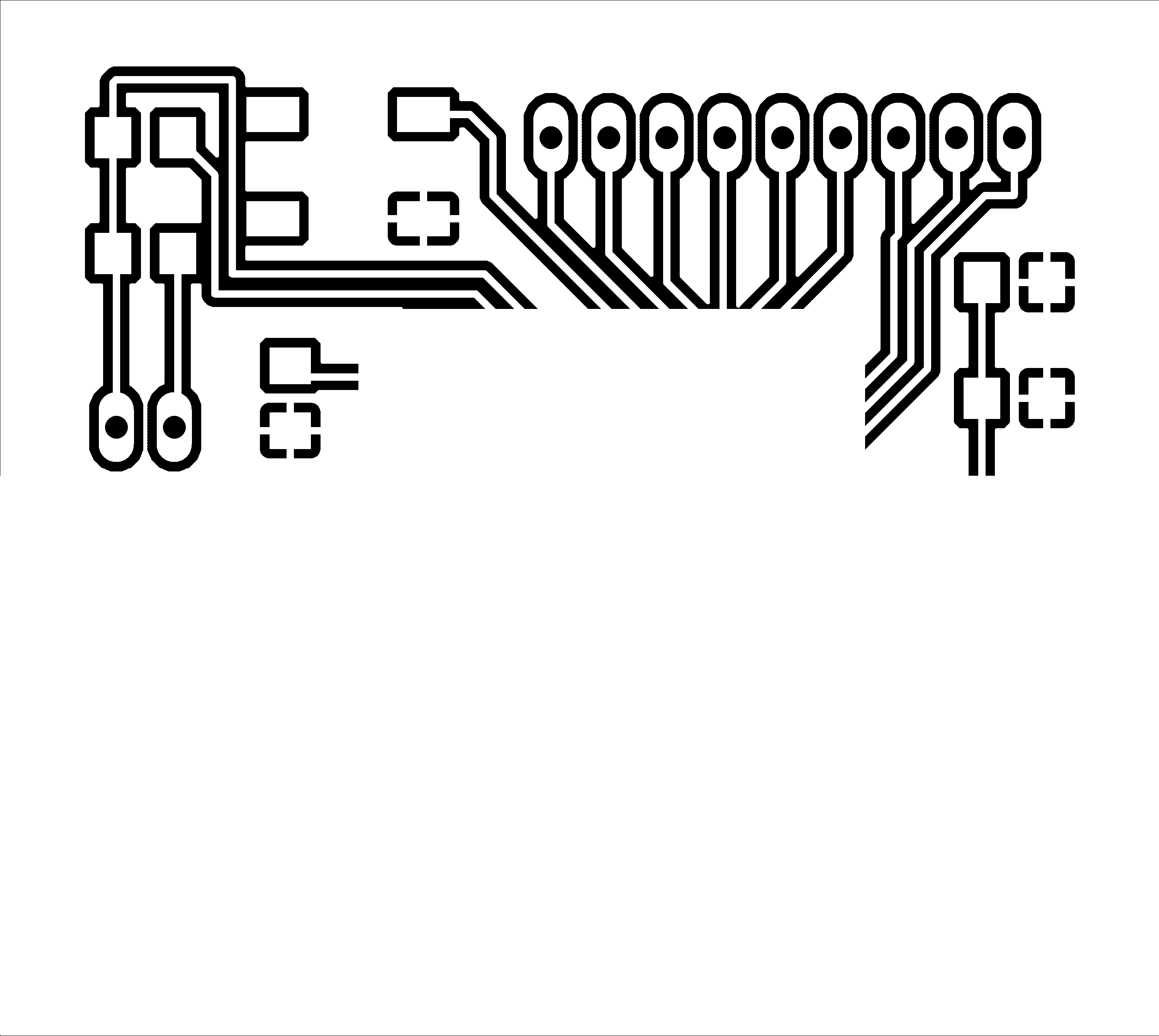 Fig.10: BW .png image of cropped traces. |
As previously mentioned, the gcodes were generated using FabModules. After choosing input format (.png image), output format (Roland mill), and the process (PCB traces 1/64), there were extremely few adjustments to be made in the parameter list: defining the exact machine type (Roland MDX-40), and setting x-zero and y-zero to 0mm (Figs.11-14). Starting the calculation provided me with 4 gcodes that I transferred to the computer that is connected to our Roland mill one by one.
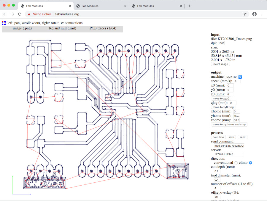 Fig.11: FabModules screenshot of traces. |
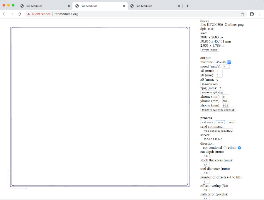 Fig.12: FabModules screenshot of outline. |
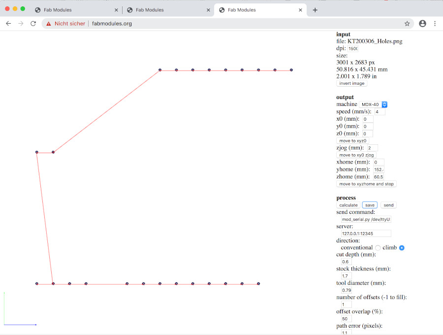 Fig.13: FabModules screenshot of holes. |
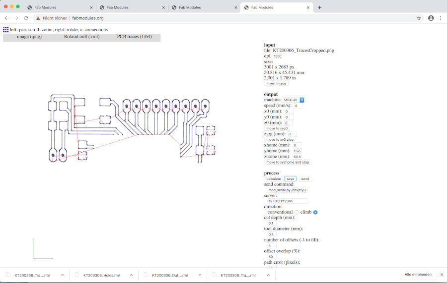 Fig.14: FabModules screenshot of cropped traces. |
After the third run, the milling eventually produced a decent enough pcb (Fig.15) which I checked under the magnifier (Lynx EVO Vision Engineering, Fig.16). This final check before soldering revealed some tiny bridges I could clean out with a tweezer (Fig.17).
I made a list of the disired components (Tab.01) and glued them with double-sided tape on paper for the final step of my assignment. Soldering still does not come easy to me, but after a lot of cursing I had my board ready (Fig.18). Although checking the traces for connection with the multimeter made some re-soldering necessary, in the end everything worked.
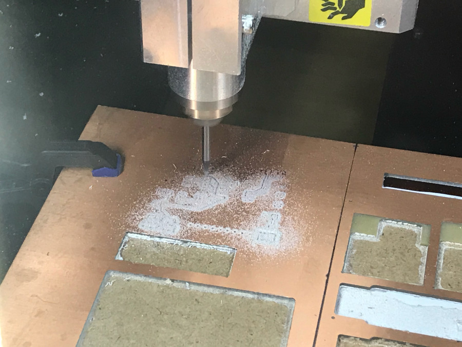 Fig.15: PCB milling process in action. |
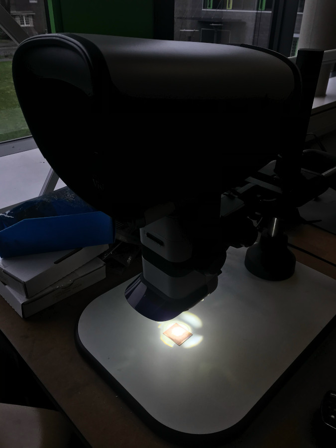 Fig.16: Lynx EVO magnifier at the FabLab Kamp-Lintfort. |
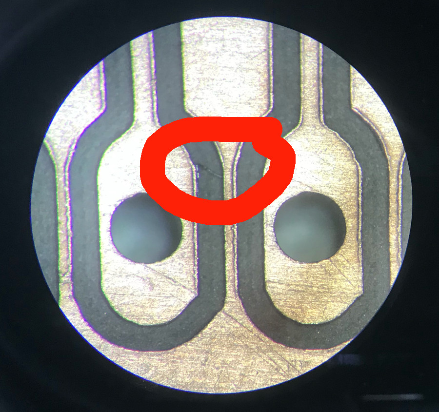 Fig.17: Magnified pad with microbridge (highlighted in red). |
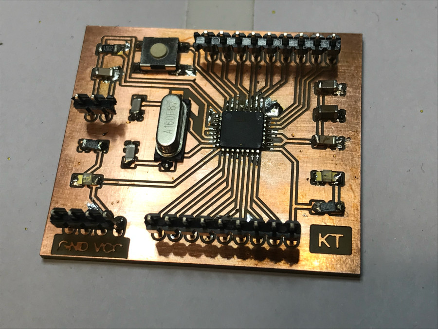 Fig.18: Soldered and error-checked board. |
Tab.01: Component list for soldering.
|
|