Embedded programming
individual asiignment
Read a microcontroller datasheet and program your board to do something
group assignment
Update 07/07/21
compare the performances and developemnet of diferent workflows
you can go here to see what i did on this week group assignment
Bloopers
if you´re looking for the individual assignment it 's below this section.
embedded programming
in order to fabricate an ISP it should be simple to solder the components, easy to programm and shoud have enough memory.
To fabricate an ISP for the electronics production class the Attiny 45 is more than enough for this task and it’s easier to solder than the ATmega328P even if this last one has 8 times more programmable memory to use.
in order to understand a little better i made a little comparison chart on MSword wich i'll be hosting here.
here you can download the comparison chart i've made during this week to define the diferences between all of the microcontrollers in our lab.
First i'd like to begin by saying that for me this was the most dificult assignment due to my lack of knowledge in programming and such basic electronic concepts.
Now that we have finished all of the modules on the Fabacademy course i 've made the design on my board but it was quite hard to make it do something.
i will divide this assignment in pieces so it has a little bit of order in the chronological order.
About the datasheet
the only thing i knew about the board i needed to design was that i needed to integrate an LCD display, three tactile buttons, one bluetooth module, one dc motor, a phototransistor and the UV lights.
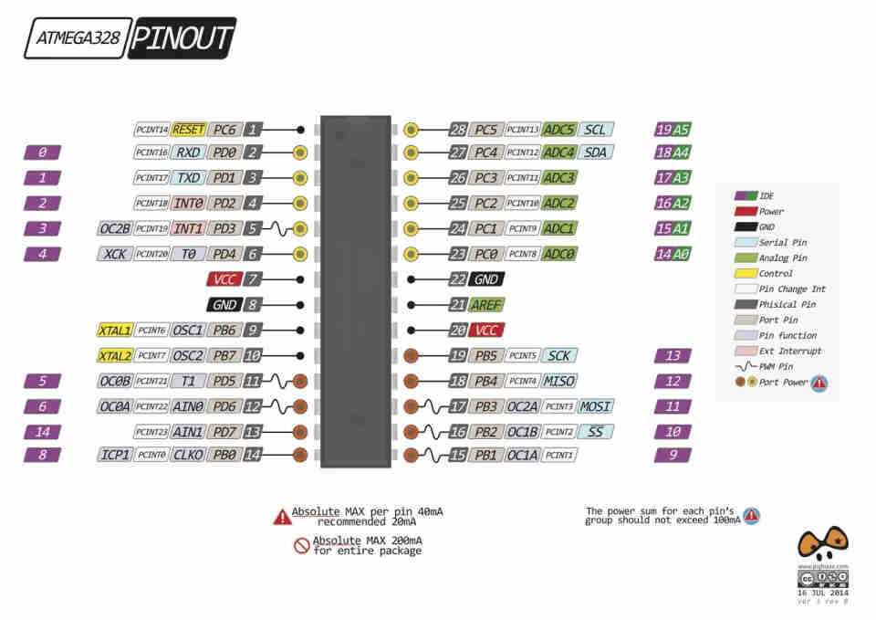
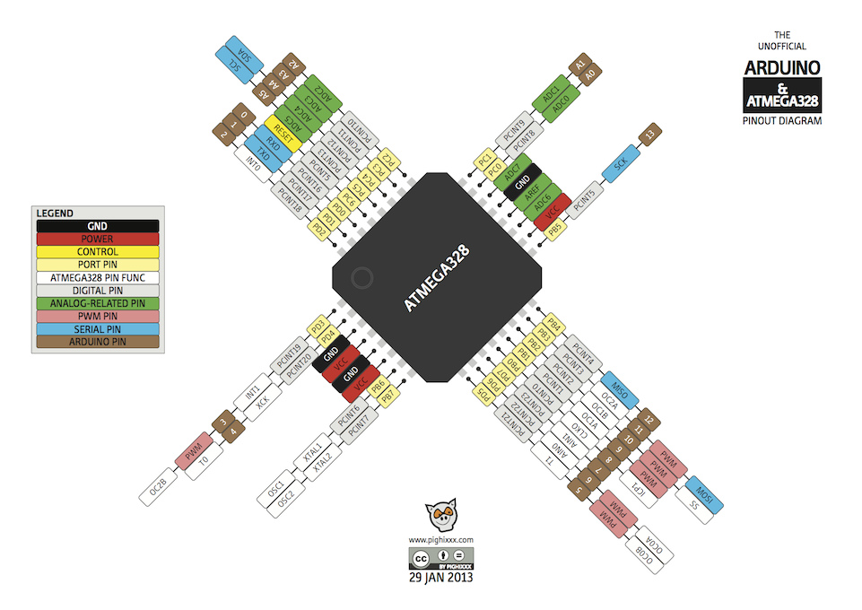
after making a comparison table on the group assignment i figured out that i needed to use the atmega 328p which i have in the lab.
this because the amount oif pins it has and the amount of memory for sketches it can hold up.
in the reference section at the bottom of this assignment you can see the link to download the datasheet.
the search
after looking how to program a atmega328p TQFP package on the internet i realized that all of the info was about the DIP package and after looking at the pins on both them figured out that was the same procedure all that changed was the pins on each package.
 Atmega328p DIP package
 Atmega 328p TQFP package
so i went ahead and designed my board knowing that i needed to integrate the board inder the motor and all of the inputs and outputs shall be all arround the machine. thats why i used diferent footprints because i needed to drill some holes in order to solder wires in the the board.because we don't have smd header in our lab yet.
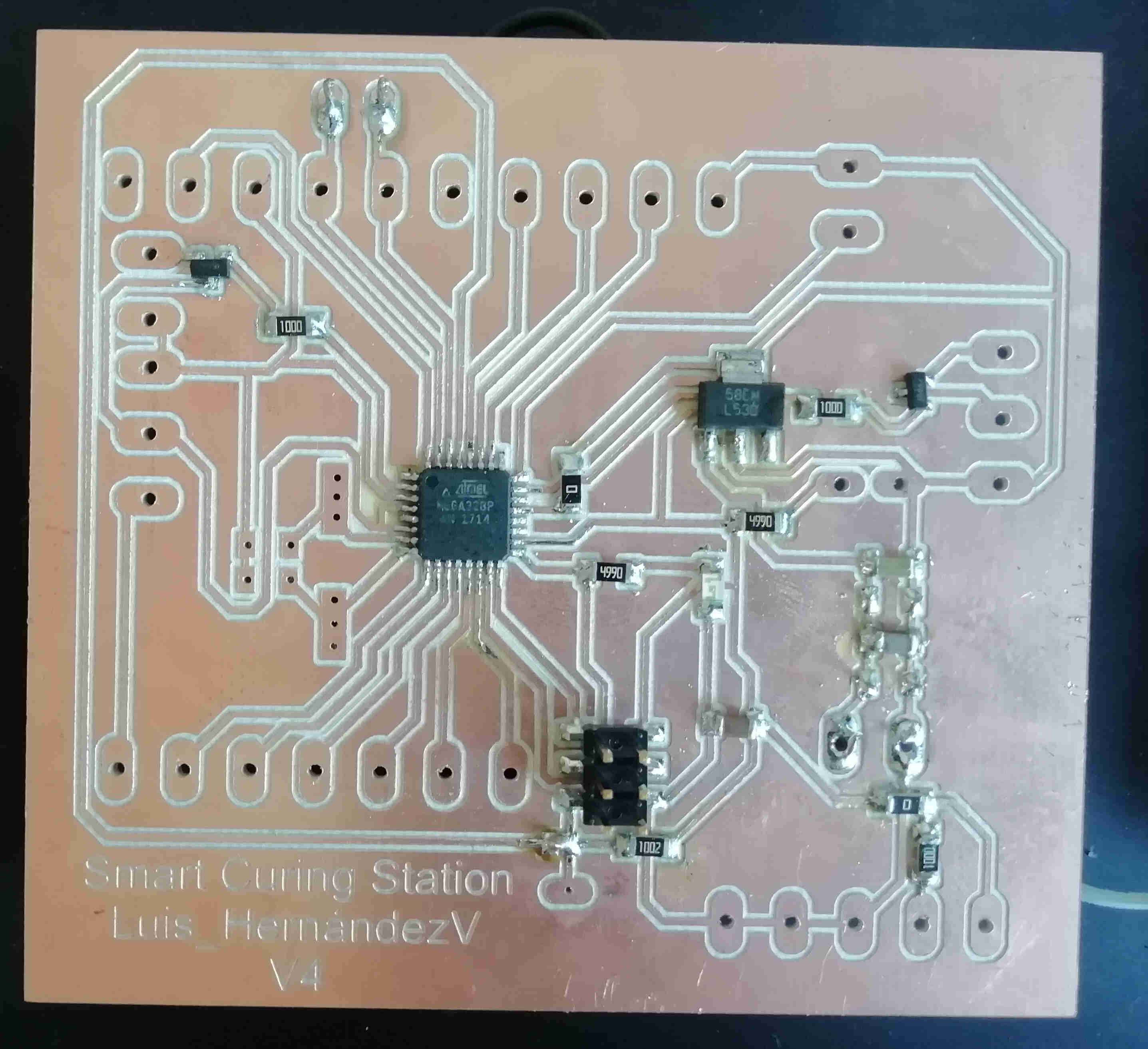 Smart Curing Station V4 control board
after milling 5 times the board finally made it to work without using external jumpers or burning the chip.
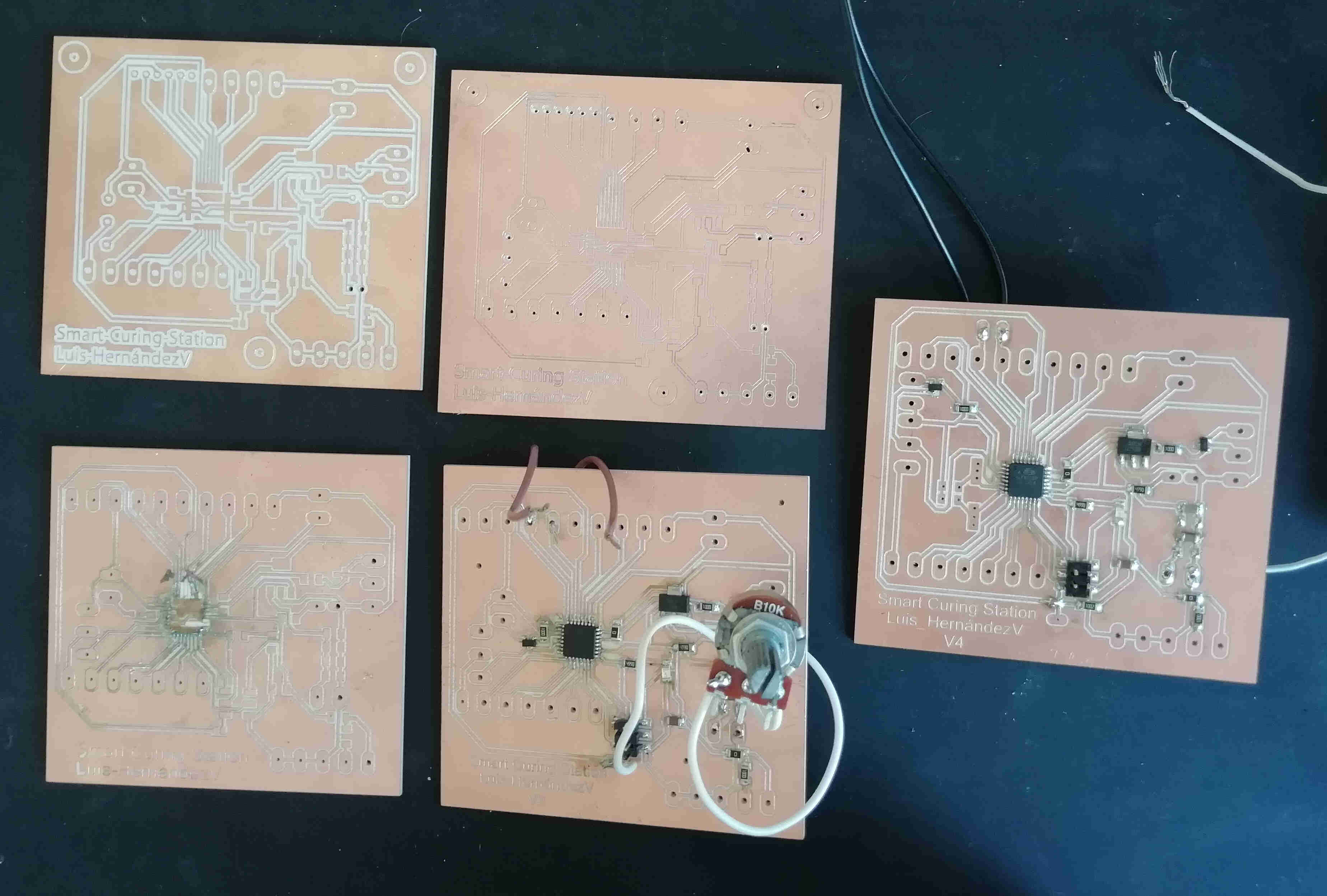 all five attempts of making the control board
a failure is only something bad when you don't learn anything from it.
in each version and failure before the V4 board i learned something thing new.
About the bootloader
i did not reinvented the wheel i just tried to apply a tutorial from a DIP package to a TQFP package.
the first thing to do with a new chip is to burn the bootloader in order to be able to load sketches on it.
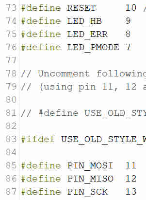
Ussually the tutorial on this topic uses the 16Mhz xtal pins as a clock. but i wantet to use the 8Mhz internal clock so i had to configure the the arduino IDE to use a diferent board than the standard arduino uno you can download the file i used at the bottom under "links and references" and here
And i made a tutorial on my youtube channel on how to "install" it on the arduino IDE you can check it out in the "links and references" section
here is just a short clip with low resolution on how to do it
video on how to install the breadboard file on you PC (using windows 10)
then you have to load the arduinoISP sketch on the arduino UNO board like any other sketch under file/examples/11ArduinoISP/ArduinoISP
load it to the board using the standard settings in my case board: Arduino UNO Port: COM10 (Arduino UNO) Programmer : AVR ISP.
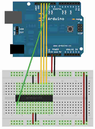
once thats done have to do the wiring acording to the sketch on the Arduino ISP like the image
 Arduino ISP variable pins
wich correspond to the wires on the ISP header on my board like this
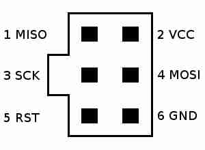 ISP Header
it looked like this in my case
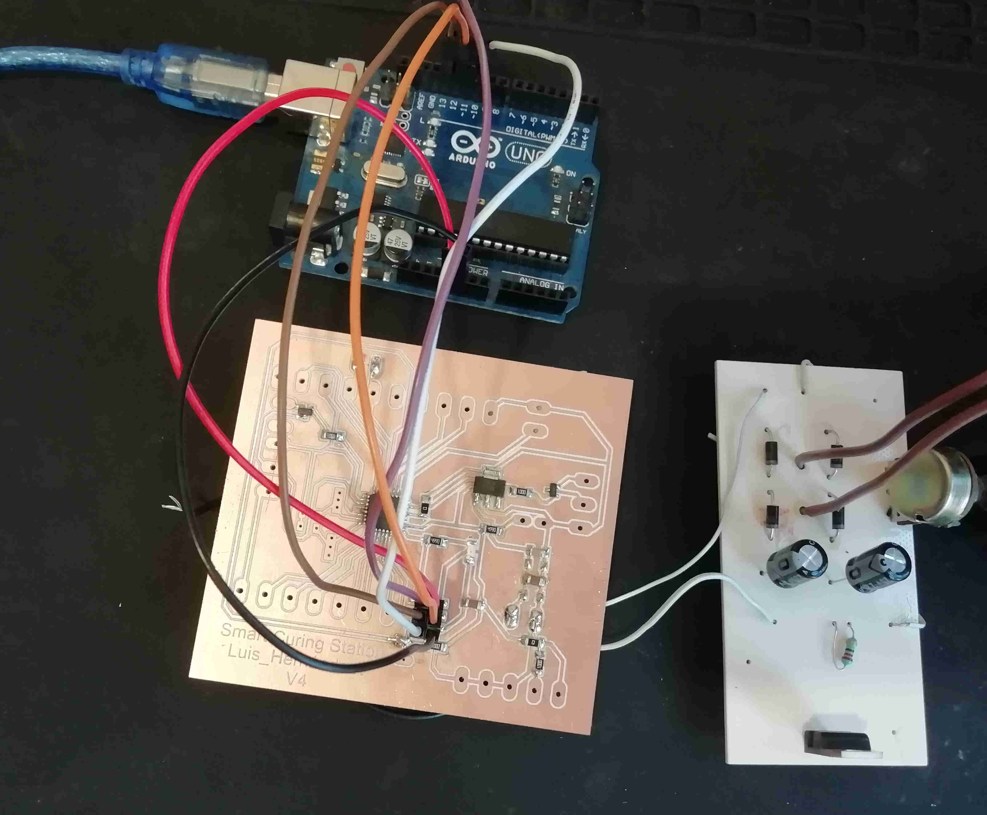 Arduino as ISP
in the original tutorial image looked like this but i used my own power supply and a diferent package
 original diagram on tutorial
Now it is time to burn the bootloader.
first thing is to change the board on the IDE under tools/ Board/ATmeega328p on a breadboard(8MHz internal clock)
then change the programmer under tools/programmer/Arduino as ISP.
now burn the bootloader by clickin on tools/burn Bootloader
if done correctly you should see a message on the arduino IDE status bar saying bootloader has been burned.
about uploading programs
since i wanted to test if the board was right i placed an LED conected to the SCK pin on the atmega328p which is the same digital pin on the arduino in (pin 13) with this Led i should load a simple blink and see it the code has been recived from the IDE.
but first i need to wire the comunication converter from the arduino uno to the board.
since i did not have FTDI headers to mount on my board in the lab i milled some holes directly to rx and tx pins on the ATmega in my board.
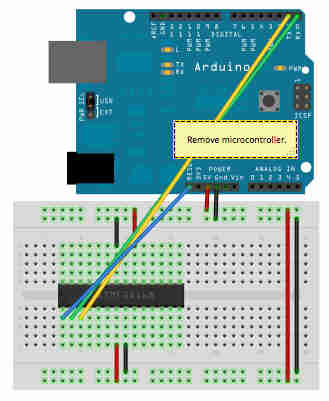
in order to use only the serial converter chip on the arduino board y need to remove the atmega328p dip packeged chip on the arduino uno board like in this video
remove the atmega328p on the arduino board to use only the serial converterthen i needed to wire the RX of my board to the RX from the arduino board .Now the TX on my board to the TX on the arduino board the RESET pin on the SPI header of my board to the RESET pin on the arduino board and the GND of my board to the GND pin on the arduino board
it looked like this in my case
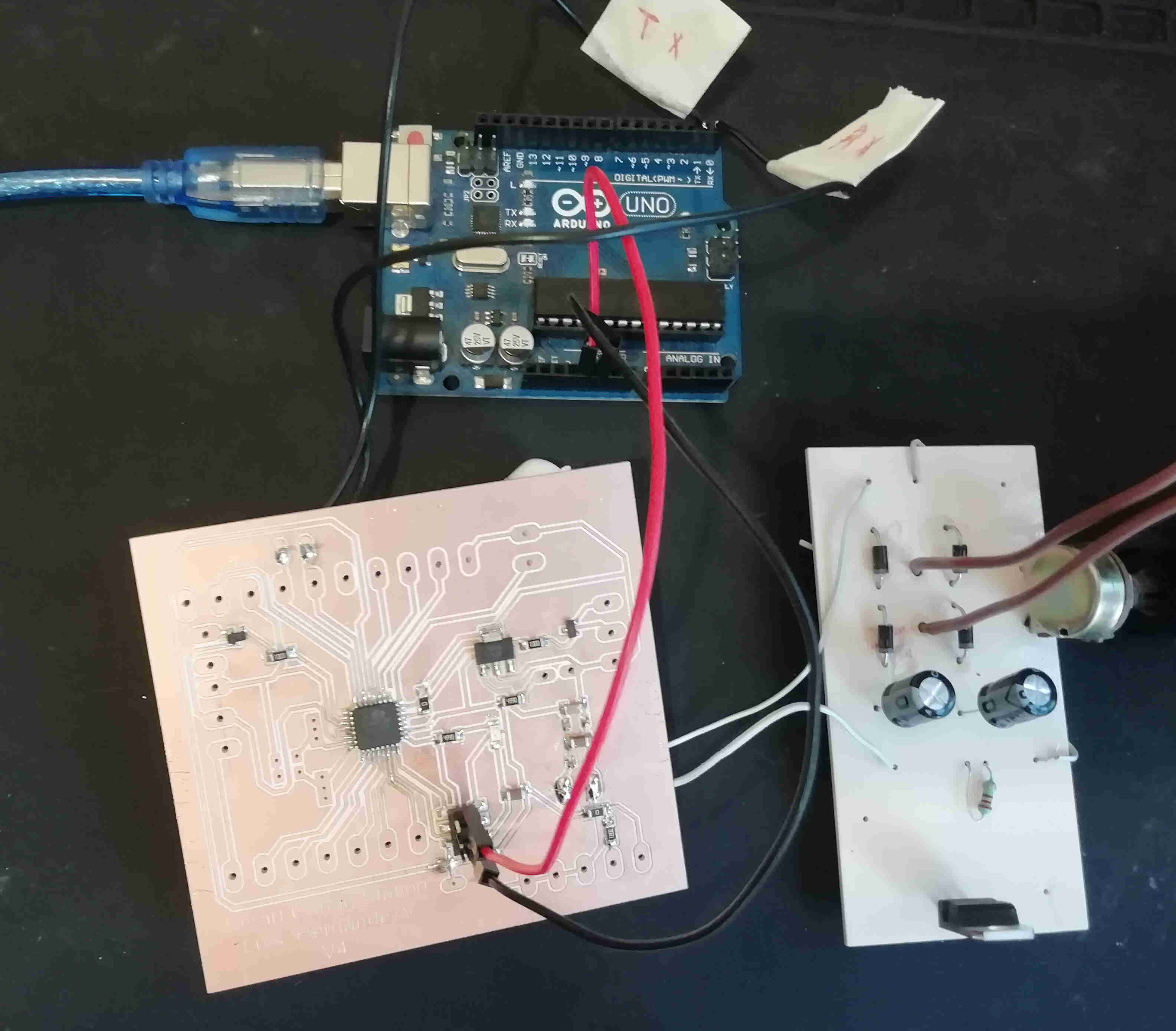 picture of the wiring while loading a program to the board
but in the original tutorial looked like this
 original diagram for loading a program
after doing all of this wiring it was time to load a program. So i opened arduino IDE once more and opend the blink code under file/examples/01Basics/blink
and load it using the following scheme board:ATmega328p on a breadboard Port: COM10 (Arduino uno) programmer: AVR ISP
after doing it right you should see the led blinking in my case it did
blinking led on my final project boardsorry i could not upload it on my repo but i could not compress it in less than 10MB.
as you can clearly see in the arduino example even had a name prewritten "pinMode(LED_BUILTIN, OUTPUT);"that's more user readable than "DDRB=32;"
HERE You can download the text file for the blink sketch using low level progamming
Even in this example are more comments (all of the text after // or between /* this is a comment */ ) than code
HERE You can download the ino file for blink i first loaded on the final project board.
HERE You can download the ino file for final sketch i did for my final project.
individual assignment
Update 13/07/21
first blink using FabtinyISP
Finally i have a completly functional USBtinyISP.
i can't wait to use it in all of my projects.
certanly the first test was to upload a sketch and that's what i did.
i used the attiny45 to make the brian's version of the ISP.
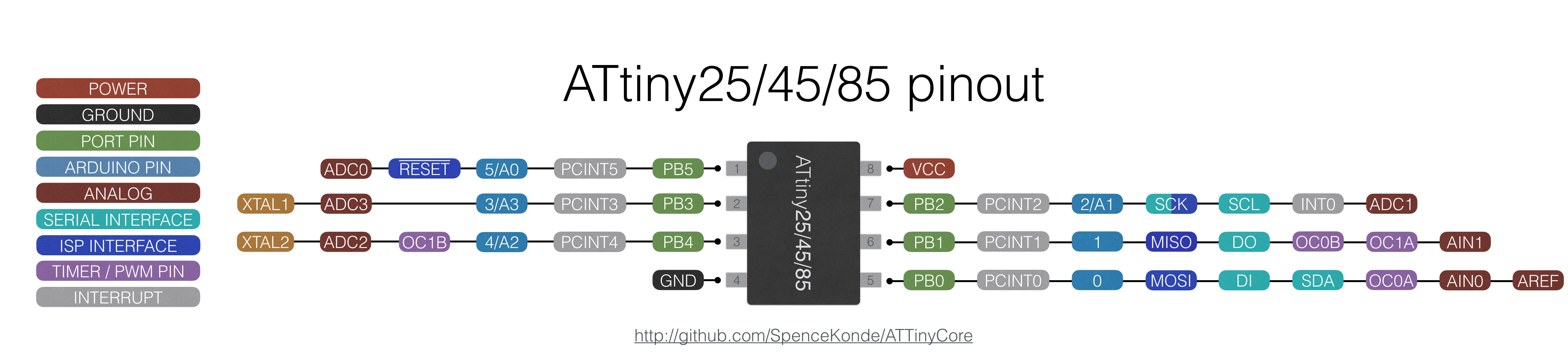
HEREyou can download picture of the pinout including the arduino ide pins for the ATtiny45
since i've already made my echo board previously but i used a dev board to upload the sketch.
and sure enough stop blinking and started using the button to control the led.
This is the code i used to control the button on my echoboard
HERE You can download the ino file for the button sketch on the video i did with the echoboard.
The design on this board and another using the attiny44 are documented on the electronics design week
conclusion
to this day a not know why on my windows 10 PC the commands refused to work properly.
I hope to get it to work on windows soon an will share it on youtube.
The diference between digital only pins and Analog/digitalPins.
the diference between volatile and non-volatile memory.
LINKS AND REFERENCES
here i will link the documents on this week assignment and tutorials.
HERE is the file i used to define the atmega 328p (8MHz interal clock) on the arduino IDE.
HERE datasheet on ATmega 328p.
HERE tutorial i followed (in english).
HERE tutorial i followed (in spanish)
HERE SPI Header Pinout
HERE FTDI Header Pinout
HERE Atmega 328p DIP package pinout
HERE Atmega 328p TQFP package pinout 1
HERE Atmega 328p TQFP package pinout 2
HERE Video tutorial on how to burn the bootloader and load a program on a standalone atmega328p dip chip
HERE my video on this
here you can download the comparison chart i've made during this week to define the diferences between all of the microcontrollers in our lab.
here you can download the datasheet on the attiny25/45/85 i used to make the Fabtinyisp
here you can download the datasheet on the attiny 24/44/84
here you can download the datasheet on the Atmega328p
HERE You can download the ino file for the button sketch on the video i did with the echoboard.
HERE You can download the ino file for blink i first loaded on the final project board.
HERE You can download the ino file for final sketch i did for my final project.
HERE you can check the repo created to integrating the attinny family to arduino enviroment
HEREyou can download picture of the pinout including the arduino ide pins for the ATtiny44
HEREyou can download picture of the pinout including the arduino ide pins for the ATtiny45
HERE you can download the text file for the over complicated blink sketch
HERE you can see a playlist of videos on how to have a better understanding on the pin adresses and types of memories and low level prgramming skills. using the ATmega328P that comes within the arduino.
HEREGIT hub repo where you can find more about the atmega328p tqfp integration with arduino IDE pins