
6.
Electronics Design
Assignments
group project
Use the test equipment in your lab to observe the operation of a microcontroller circuit board (in minimum, check operating voltage on the board with multimeter or voltmeter and use oscilloscope to check noise of operating voltage and
interpret a data signal)
Document your work (in a group or individually)
individual project
redraw an echo hello-world board
add (at least) a button and LED (with
current-limiting resistor)
check the design rules, make it, and test it
extra credit: simulate its operation
Download files
Download all the files from this week's adventure.
Download all filesTable of contents
-
Introduction
-
Designing a PCB Board
-
Digitising your design
-
Eeschema in Kicad
- For most of this I followed the (loose) instructions on the local lab’s page.
- Laying out the ATtiny1614 and other components we’ll need
- Calculating the resistance needed for the RGB LEDs
- Calculating the resistance needed for the buttons (not essential)
- What is Common Anode and Common Cathode?
- UPDI is missing? Modify the FTDI component with fab.mob and fab.lib
- Wiring them up in Eeschema
-
Send the board for layout and trace in PCBeditor
- Understanding which elements connect with which
- Shortcuts (U, E, M) & using the Route Tracks tool
- Pre-defined sizes for track & Grid snap
- Comparing size of physical components to the real size on screen (button and switch were too big)
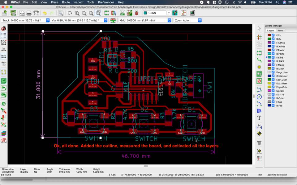
- Drawing the outline / routing of the board
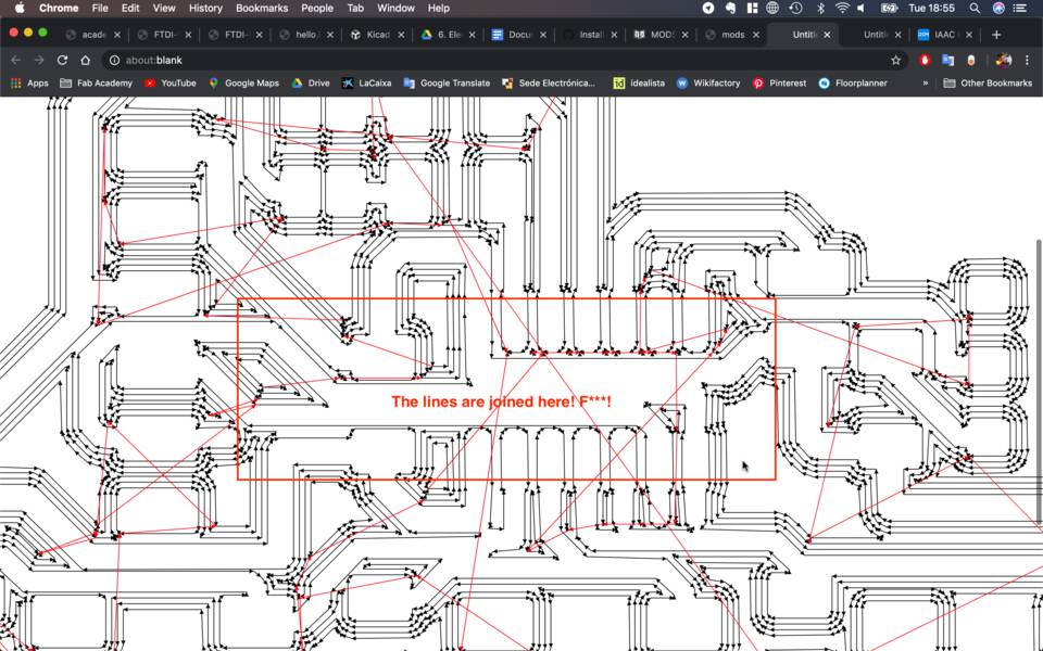
- Noticing the traces are too close and they join
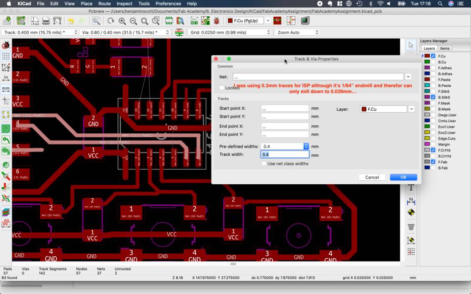
- Making the traces for the entire board 0.4mm
- Adding a jumper to solve all the problems
-
Creating the files to the milling machine
-
Soldering the board
-
Programming the board
-
Have you?
Group assignment
We didn't get to do the group assignment as COVID-19 decided to come along and close down the Fab Lab.
Unfortunately I don't have a spare oscilloscope or logic analyser on me to analyse the microcontroller I have.
Introduction
My final year project idea is a SmartWindow which switches on depending on the weather and time of day outside, using either RGB LED strips or just a mix of warm white and cold white LED strips.
Let’s have three buttons that can control the RGB channels of an LED. Each time you press a button it increases how fast the color channel of the LED it is associated with blinks and therefore how bright it is.
Designing a PCB Board
Thinking and theory
Three buttons that each control an RGB channels of an LED
- Components needed for the circuits:
- 3 x buttons (temporary switches)
- 1 x RGB LED
- 1 x switch
- 7 resistors (for each element above)
- 1 capacitor between VCC and GND to smooth out interference
Drawing up the layout of the board
From the start I knew I needed 3 LEDs and 3 buttons, and that they needed to wire them to inputs and outputs of the boards.
It’d be simple: connect one end of the LEDs to an OUTPUT, which would act as VCC and then connect the other end of the LED to a resistor which then goes to GND… easy. For the button I got confused…
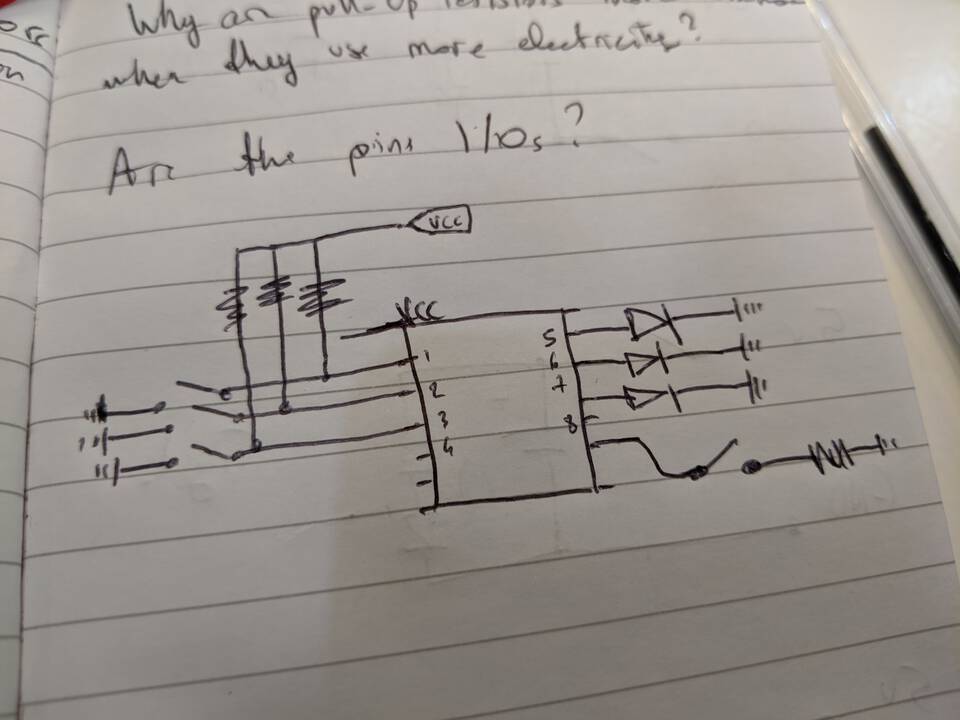
How to wire 3 buttons through with one common VCC source?
I got confused because we’d need to wire a circuit between VCC and 3 inputs (with a resistor, of course) so that the inputs stay in HIGH mode.
Then when you press a button the current “ends” its journey into GND… but the start of the current for all 3 circuits comes from the same VCC... Doesn’t it mean that when one button is pressed then the current from all the inputs gets “sucked” into GND as well, and therefore change to a LOW value?
That’s when I read this article and this article about pull-up and pull-down resistors. It was a very interesting read which helped me understand a lot how the circuit and chip works. It says that the I/Os in the chip also have an internal resistor, called input impedance. It usually has a very high resistance.
Below is a drawing of how the current travels through the circuit when the switch is closed or opened. On the
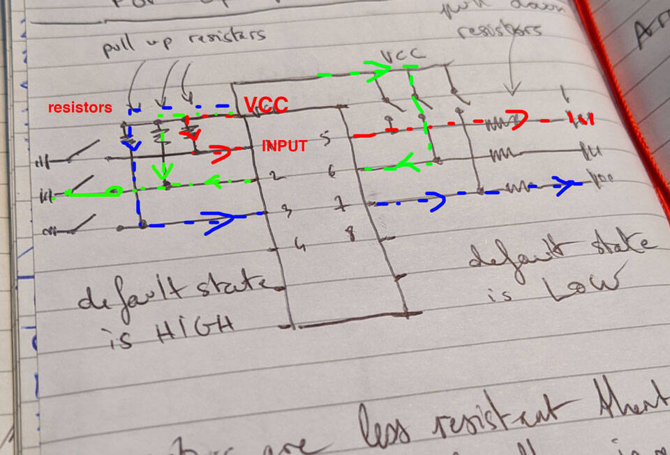
A question… ?
I had a question, which went something like: “Why are pull-up resistors the most common one when it means you keep the state of the pin as HIGH all the time rather than keeping it as LOW? Doesn’t it consume more power?”
Oscar answered something like: “No, it actually doesn’t consume any power, it’s just the state of the pin that is HIGH. It has voltage going through, but it doesn’t actually use it for anything”.
Choosing the ATtiny1614
I chose the ATtiny because it has 9 I/Os which allowed me to have 3 for each button and 3 for the LED's RGB channels. Then I used another one for a switch, because why not.

If you search “Ratings” it shows General Operating Ratings under the Electrical Characteristics header.
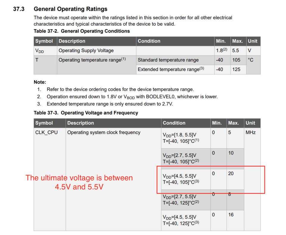
You can see that it’s optimum range is from 4.5V to 5.5V, in other terms at 5V.
You can see it’d work with a voltage down to 1.8V, which would result in the MCU running at a speed of 5MHz. As we have a very simple circuit we could work with that, but because we might use the board later for more advanced functions, we’ll stick with 5V.
Note //
That’s also the power that provided by USB, and therefore it avoids from having to convert the power.
Digitising your design
Eeschema in Kicad
I followed the (loose) instructions on the local lab’s page
The tutorial runs you through everything from installing the libraries of components, to placing them in the Eschema and then connecting them in PCBeditor.
Laying out the ATtiny1614 and other components we’ll need
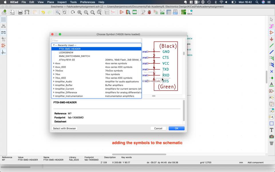
Adding symbols to the schematic.
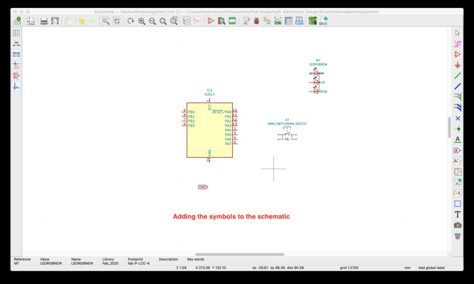
The Symbol window.
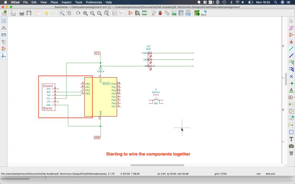
Starting to wire the board together.
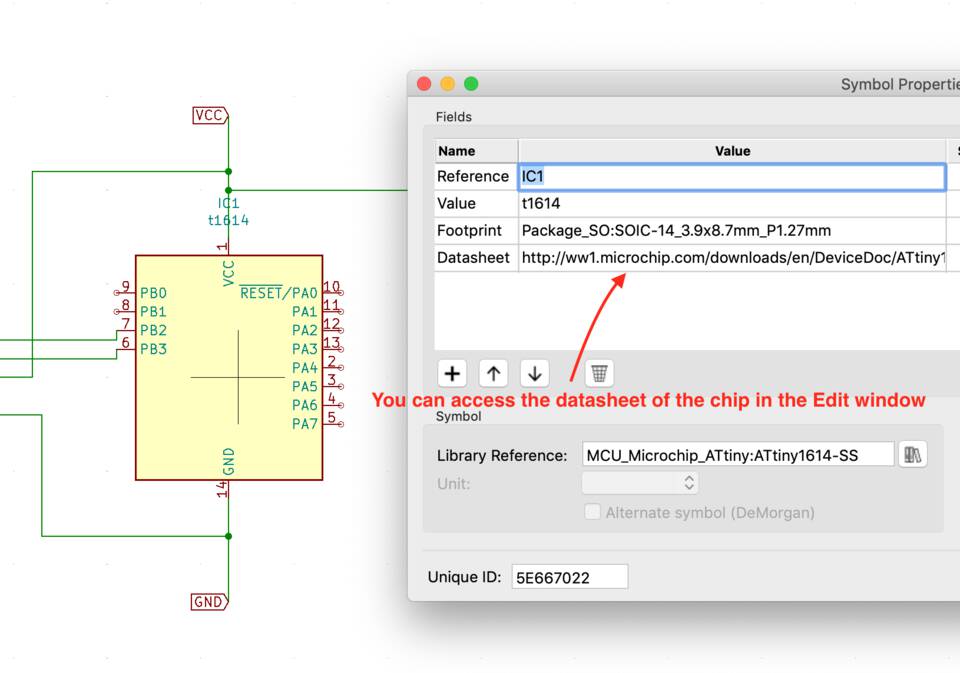
Pressing the E key over a component shows its value. In the ATtiny1614 componenent you also have a link to its datasheet.
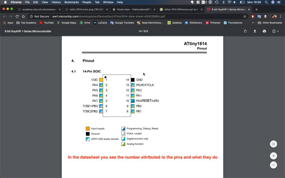
In the datasheet there is all the information you could possibly need to know about the chip. There are also the I/Os layout so you can connect them properly on Eeschema. On Eeschema the VCC is on top, the GND is at the bottom and the I/Os are on both side.
Adding and calculating the resistance needed for the RGB LEDs
Below is the amperage consumption of the individual LEDs in the RGB LED. You notice that the red led consume twice as much as the other two.

Ohm’s Law says that V = I * R, where V is in Volts, I in Amps and R in Ohms. The figures from the datasheet are in mA and therefore need to be converted in Amps for the equation.
We want to calculate the Resistance needed, so we can flip the equation around to R = V / I.
RR LED = 5 / 0.05 = 100Ω
RB&G LED = 5 / 0.025 = 200Ω
Here we are. We need to use 100Ω resistors for the red LED, and 200Ω for both the green and blue LEDs.
Calculating the resistance needed for the buttons (not essential)
The general rule is to use a pull-up resistor (R1) that is an order of magnitude (1/10th) less than the input impedance (R2) of the input pin.
Quote from Pull-up Resistors - learn.sparkfun.com
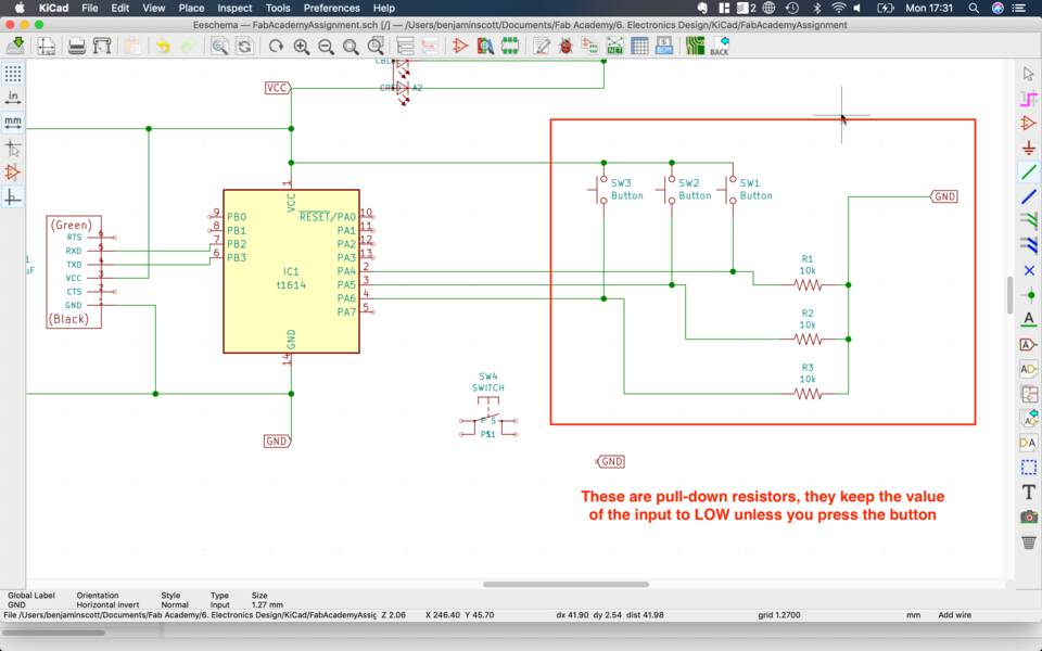
It doesn’t need an exact resistance as all it needs to do is avoid the circuit to short. A common value to use is 4.7KΩ.
If you use a resistance that is too high, the pin might take longer to register the change in value, and that is not good for circuits that need speed. If you use a resistance that is too low it will consume unnecessarily amount of power for such a simple task, and possibly create a short / burn the pin.
What is Common Anode and Common Cathode?
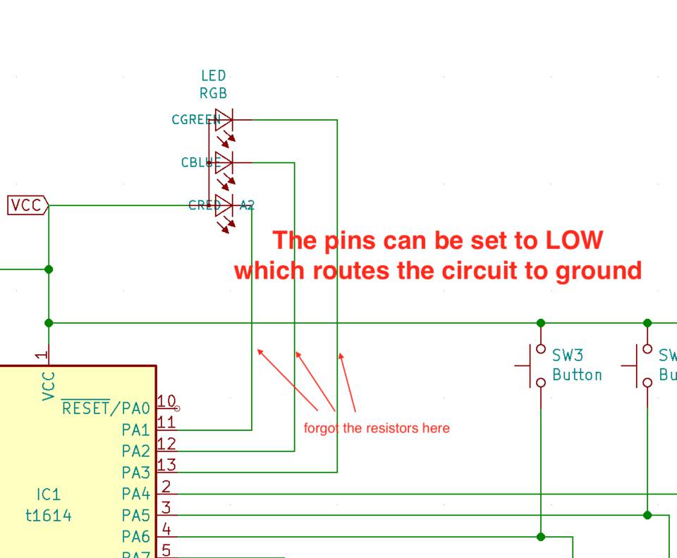
The one that is given on the Eeschema is a common anode one, which means that the three “feet” for the channels go to GND. I thought that if you wanted the channels to light then you’d need to connect it to ground with a switch… but that switch would then need to be controlled programmatically via the I/Os.

I asked Oscar but he said that the pins by default act as VCC, but if you put them to LOW then it acts as a ground, so you only need to connect the cathode side of the LEDs to the I/Os to control the channels.
UPDI is missing? Modify the FTDI component with fab.mob and fab.lib
There wasn't any Symbol or Footpring for the UPDI in the Fab Library. I asked Josep what was up, and he explained how to modify the FTDI component to create the UPDI. I screenrecorded the conversation we had.
Wiring everything up in Eeschema
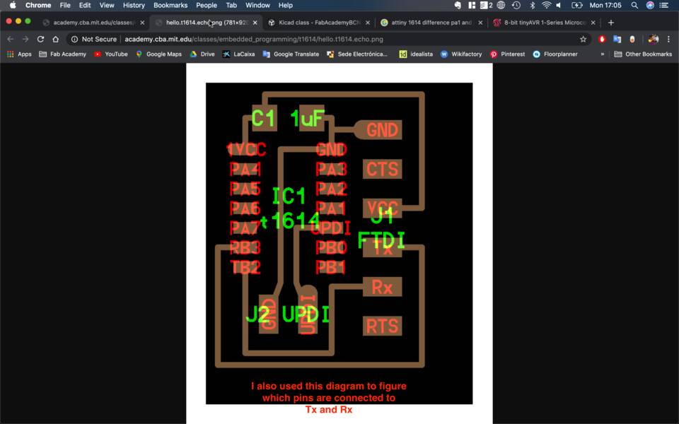
I used the image below to figure which pins needed to connect where, at least for VCC, GND, TX, RX & the RESET pin.
After wiring up all the components in Eeschema.
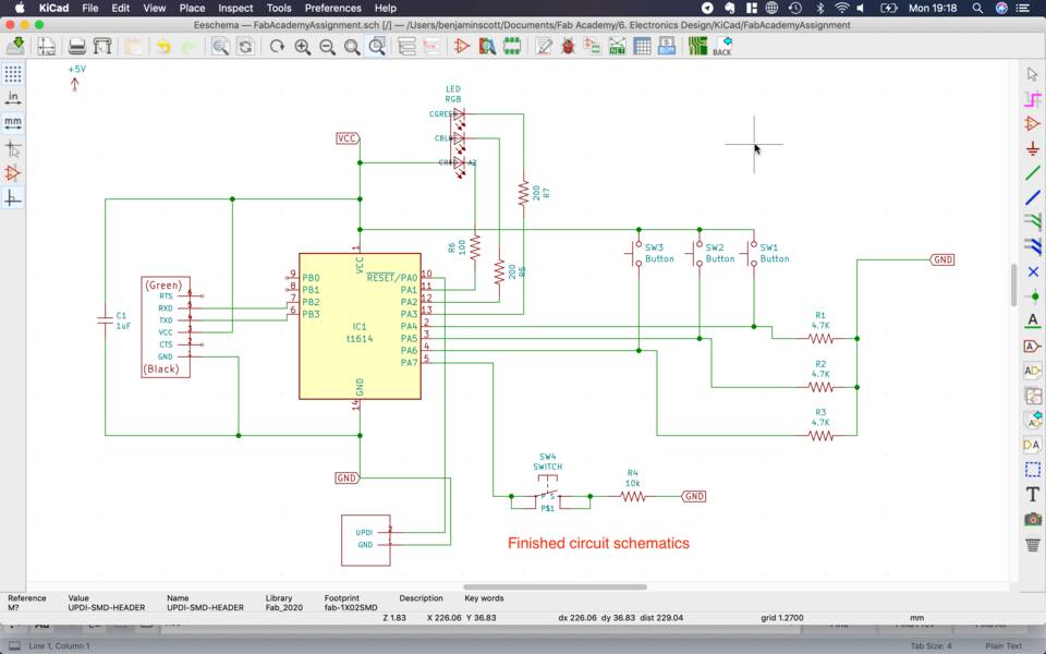
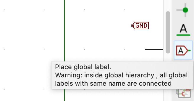
I didn't realise that if you did it in different part of the window, and used the Labels it actually joined them. I thought it was just for clearing things up. It didn't bother me too much though as it isn't a very complex board.
Send the board for layout and trace in PCBeditor
Understanding which elements connect with which
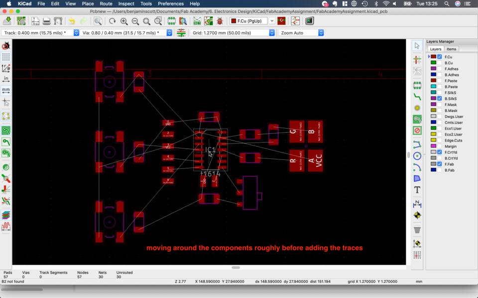
It took me a little while to understand why when you moved the elements, the white lines connect to different pads... I was confused because I thought "well... the resistor has to go this pad, and then to ground, why is it jumping around like there's different options?"
Then I understood that GND need to be connected EVERYWHERE on the board, and therefore the white line just automatically jumps to the closest GND available.
That being said, I started moving the parts around to recognise what was what, and see where it'd make sense to place the components.
Shortcuts (U, E, M) & using the Route Tracks tool
There a few shortcuts that really saves time. While hovering above components tap:
- E to Edit the component such as it's Reference and Value.
- M to Move the element and click to Release
- U to Select the entire wire you are hovering over
- Delete (not Backspace) to Delete the element or a section of wire
Pre-defined sizes for track & Grid snap
In the drop-down menu at the top left that says Track you can enter pre-defined sizes. To play around, I decided to create different tracks, for different components. For example if it was connected to VCC or GND, then the tracks would be 0,6mm wide, as it handles, albeit little, power.
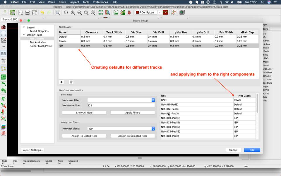
I also created width of 0.4mm for normal traces and finally 0,3mm for traces that were connected to the ISP.
I later realised I shouldn't have done that.
Comparing size of physical components to the real size on screen (button and switch were too big)
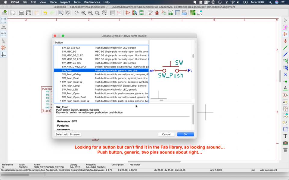
When in Eeschema I looked for a button but couldn't find one in the Fab library, so got one from the Kicad one.
In PCBeditor you can set the Zoom ratio in a drop-down menu in the top-right. If the Zoom is 1, then if you place your component in front of the screen, it should be the same size. (For some reason I couldn't set the Zoom exactly to 1, but the closest was 1.38)
I compared the real life button to the one I picked, and noticed it was waaaay too big. I then searched in the Fab library and found a button called 6MM_SWITCH. This one worked.
Same problem with the RGB LED. I used the LEDRGBNEW in the Fab libary and it appeared enormous on the board. I used LEDRGBOLD instead and that was the right LED.
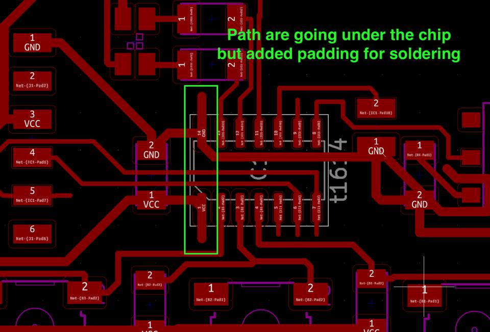
Traces going under the chip
For a cleaner and smaller board I made some traces go under the ATtiny1614. The problem with that was to solder the pins to the traces that goes under it... so I added little pads to ensure the connection, but also make sure it doesn't move.
Drawing the outline / routing of the board
Noticing the traces are too close and they join
Making the traces for the entire board 0.4mm
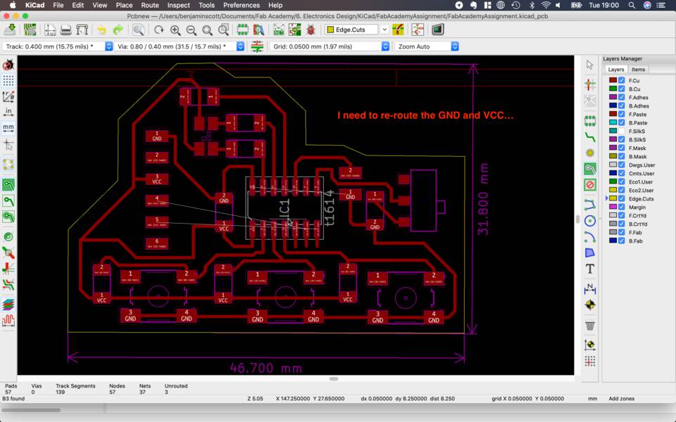
Adding a jumper to solve all the problems
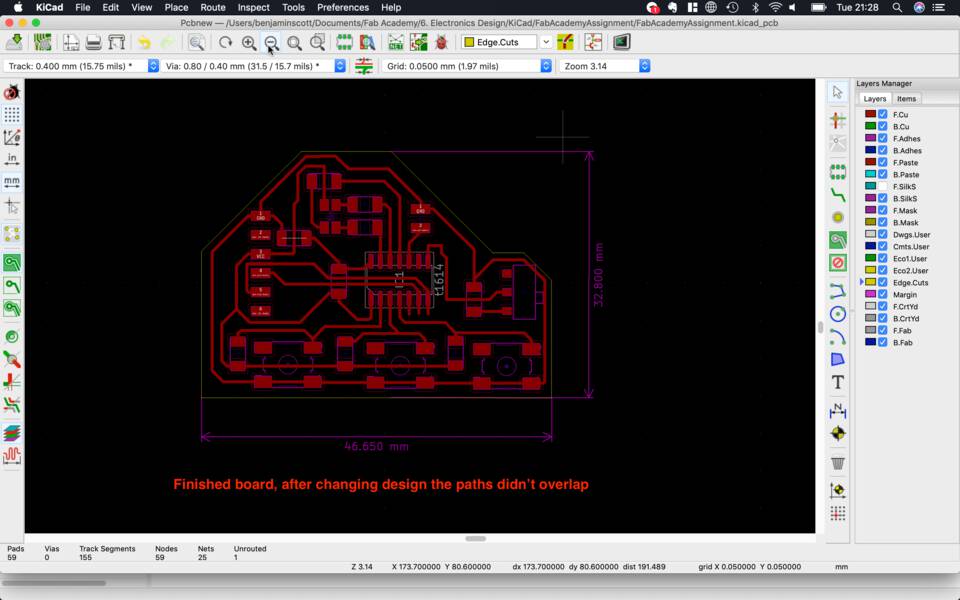
Creating the files to the milling machine
Export to SVG with these settings
Installing Inkscape on Mac OS Mojave
It fails, but you can install with Homebrew and a few tweaks: https://github.com/caskformula/homebrew-caskformula/issues/83
Edit: It doesn’t work. (That’s the problem of instant documentation, you see.)
Import SVG in Photoshop (Inkscape didn’t work and Illustrator was buggy)
Create the black and white PNGs for mods
Making the RML file and milling the board
We’ve done this before, see Week 4 - Electronics Production
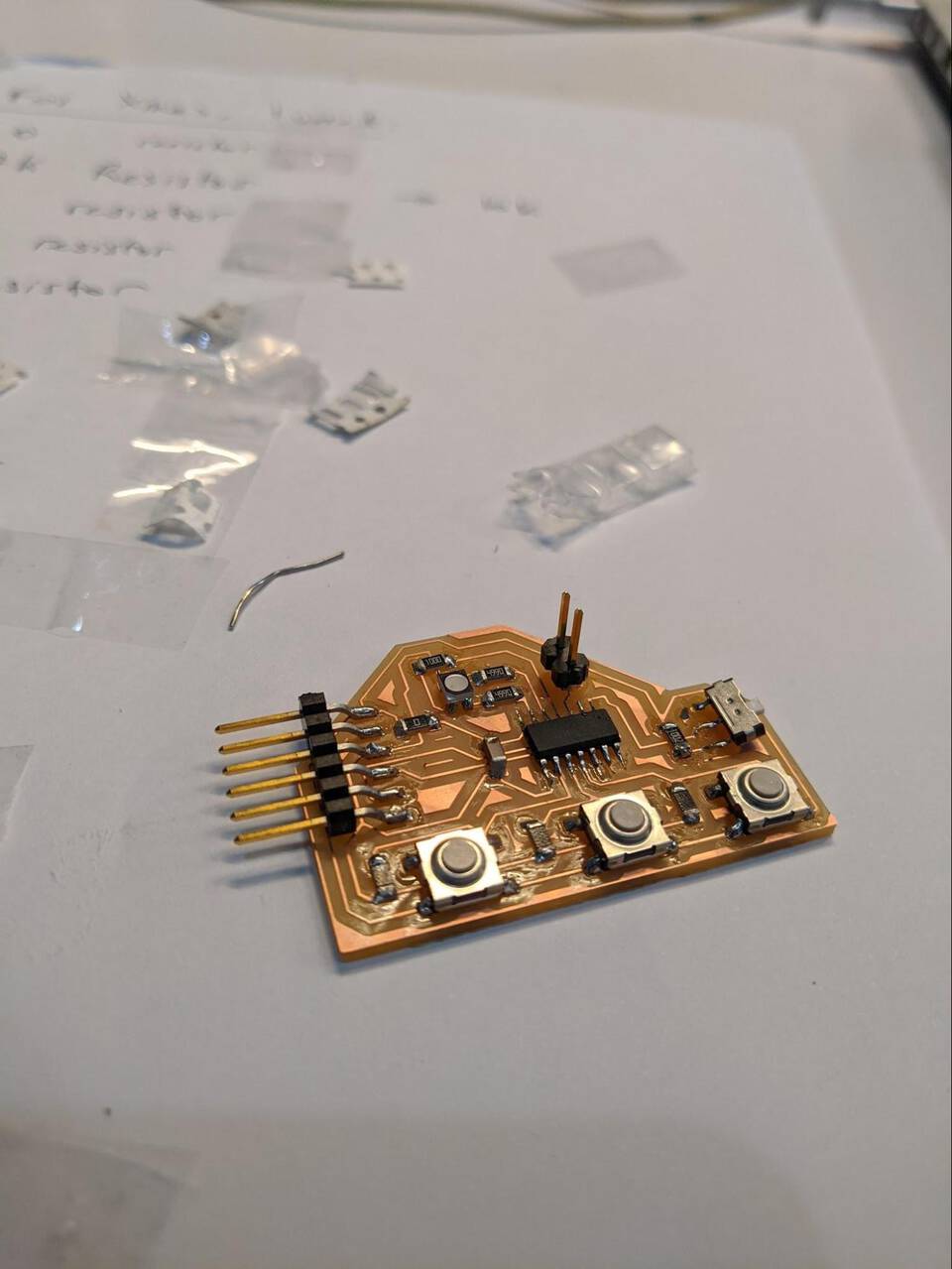
The board came out nicely.
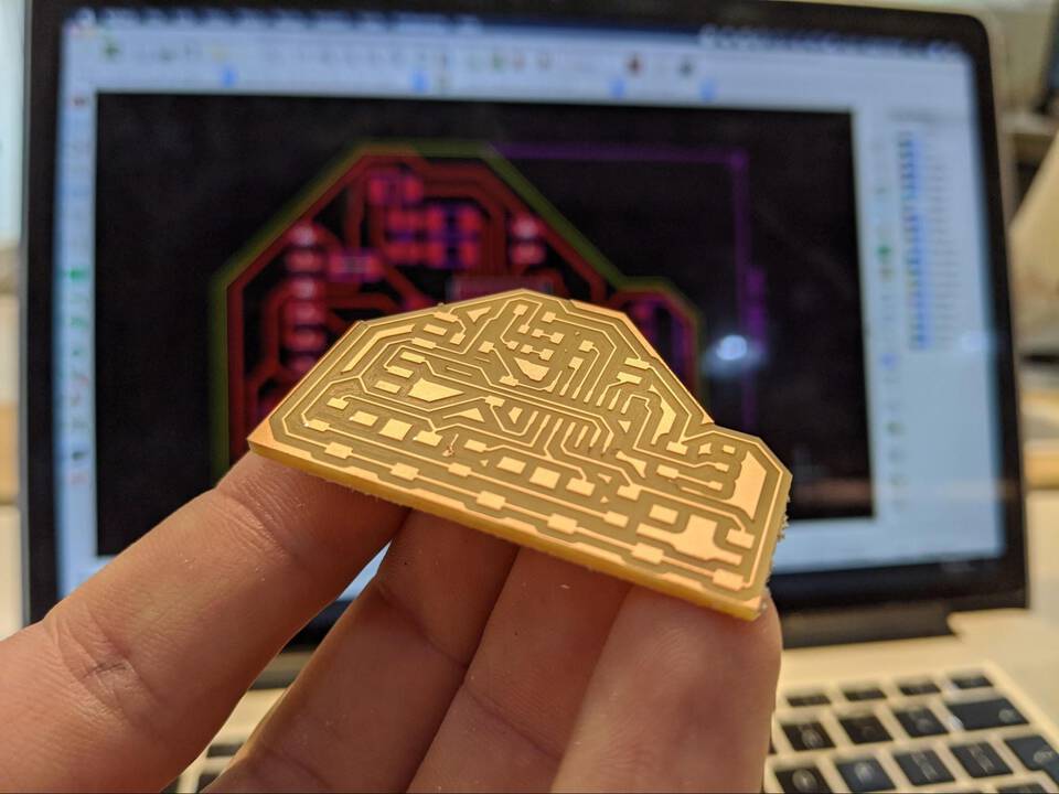
Soldering the board
Picking up the components
I check my schematics and write down the components I need.
- They are:
- 1 x 0 Ω
- 1 x 100 Ω
- 2 x 200 Ω
- 3 x 4.7K Ω
- 1 x 10k Ω
- 1 x 1μf
- 1 x RGB LED
- 3 x 6mm buttons
- 1 x slide switch
- 1 x UPDI (2x header conn)
- 1 x FTDI (6x header conn)
- 1 x ATtiny1614
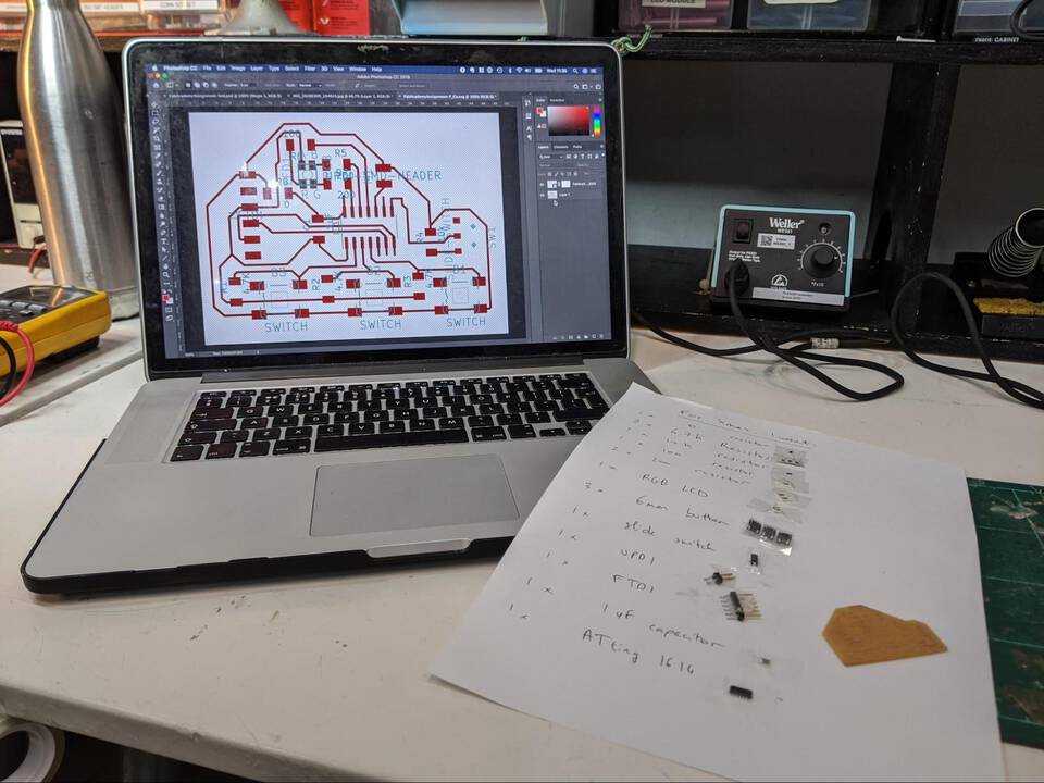
While looking for the components Daniel told me to take the 1000pF for the 1uF capacitor... Luckily I checked and it wasn’t right. 1uF is 1,000,000 pF. 1000 pF is 1 nF, which would have been at thousand times too little.
In what order?
They say from small to big, inside to out.
In order from smallest to biggest it goes: resistors, capacitor, LED, slide switch, ATtiny, UPDI, FTDI and buttons.
In order from center to outside it goes: ATtiny, capacitor, resistors, RGB, UPDI, slide switch and buttons.
I think the best bet is to start with the ATtiny, then the capacitor, then the LED and its resistors, then the resistors for the buttons, the resistor for the slide switch, then the slide switch itself, the UPDI and FTDI and finally the buttons.
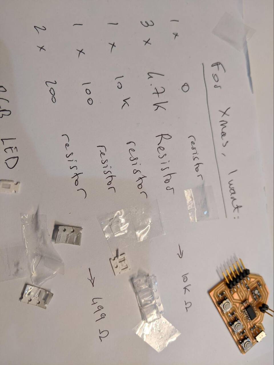
They didn’t have 200Ω resistors (whaaaaat) so I used 499Ω.
They didn’t have 4.7k either so used 10K
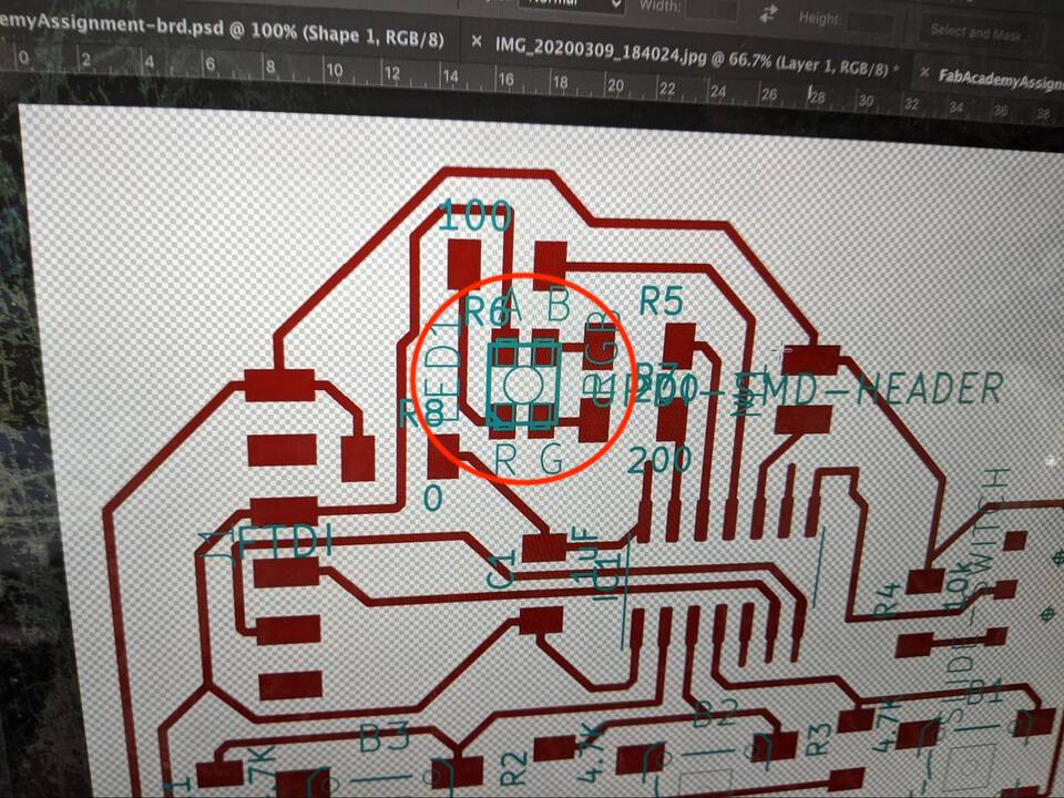
Checking how to solder the RGB LED
The RGB led has a corner that is chamfered which shows which way it needs to soldered on the board.
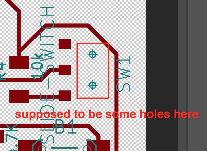
Noticing the two holes missing to place the slide switch
The slide switch has two little pieces of plastic that comes out on the bottom which is suppose to go in the board. They are there so that when you slide the switch it doesn't put stress on the soldering, but on these two protruding plastic cylinders.
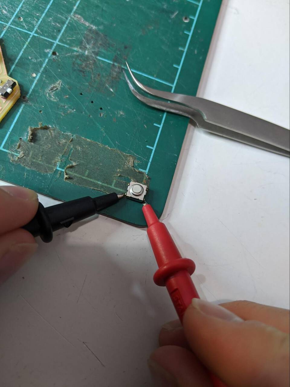
Checking the continuity on the button
To find out which way to solder the button I used the Continuity mode on a multimeter to touch the different pads of the button. If they beep then they need to be soldered on the same side, for example both to GND.
Bending the legs of the UPDI
The UPDI is simply two of the FTDI legs. The thing is, on my board it couldn’t lie down because then it couldn’t be plugged in. One solution is to bend the legs so the UPDI faces up. I decided to cut them partially instead. The result is a bendy UPDI which doesn’t seem very solid... but if you are careful I'm sure it'll work.
Finished board
I’m quite happy with the result. Not as much shininess as during Electronic Production week, but still good stuff. Plus I designed this one.
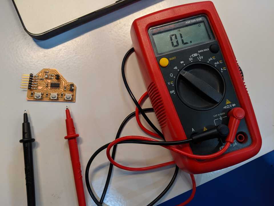
Checking continuity between GND, VCC and I/Os
I checked the continuity between the all the GND on the board, especially on the chip and FTDI. Then did the same with the VCC, and then checked one by one that there no shorts between the pins of the chip itself.
Programming the board
I forgot my board at the lab
Unfortunately, again, I forgot my board at the Fab Lab, so I haven't had time to test it. I have a Barduino 2.0 I'll be playing with in the following weeks though.
We are now the 22nd of September and I am finally going to program that board… it has been a journey since I made this board, we had confinement and the rest of the fab academy in between so it’s weird to come back… but I’m glad I did document this, because I just went through what I’ve documented so far and I’m pretty much up-to-date on what I need to know to program it.
Let’s do it.
How to program with UPDI?
There are different ways. In Electronics Production week we made different programmers, including a UPDI one… which I didn’t make.
You can also program it through the Arduino board, I found a tutorial that seems pretty good.
What I understand now is that the FTDI cable is actually just to power the board, it isn’t needed to program the ATtiny. What a waste of cable.
The video pretty much follows this link, so I shall just follow it too.
Which resistor to use?
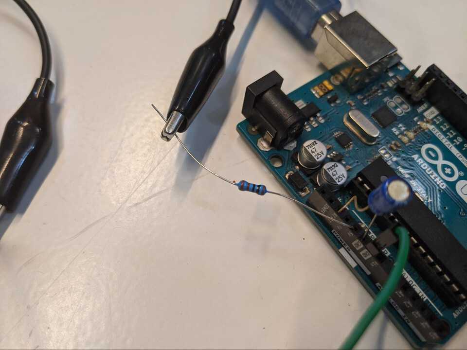
The video said to use a 4.7K resistor, as well as half of the documentation on the Git repo, but here the guy says it’s actually inappropriate and dangerously close to the upper limit of the resistor. He recommends 2 x 470Ω resistors, so I’m going to use 1 x 1kΩ.
P.S. couldn’t find one so I used 1 x 470Ω
Install the megaTinyCore board library
You have to add the megaTinyCore board library to the Arduino IDE. Add this link to the Arduino IDE in Preferences > Additional Boards Manager URLs: http://drazzy.com/package_drazzy.com_index.json
Install jtag2updi on the Arduino.
The title pretty much says it all. Download the git repo, open the .ino file. It’s empty but it links to all the other files. Upload it to the Arduino Uno (or Nano). Of course choose the right board and port.
Add a capacitor in between RST and GND
From what I understood you need to add a capacitor between the RST and GND pin on the Arduino so that in the future when you want to program the ATtiny1614 you don’t actually program the Arduino but go through it.
Wire it all
I followed the tutorial, PIN6 of the Arduino is the UPDI pin with a resistor in between, and of course 5V is VCC and GND is… ground.
Code it all
Just to test it I made a simple script. I wired PA1, PA2 and PA3 to the cathode of the RGB channels of the LED.
From the schema below we can see that they are respectively pin 8, 9 and 10.
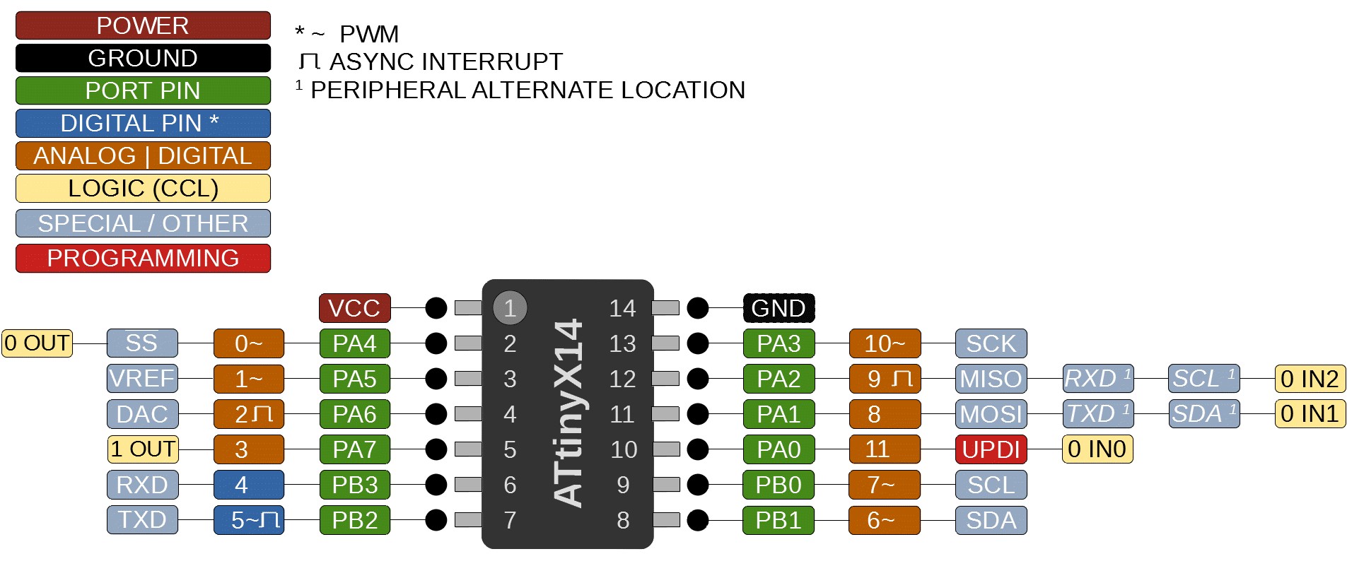
Then write a simple script like
void setup() {
  pinMode(9, OUTPUT);
}
void loop() {
  digitalWrite(9, LOW);
  delay(1000);
  digitalWrite(9, HIGH);
  delay(1000);
}
I tried to upload but it didn’t work…
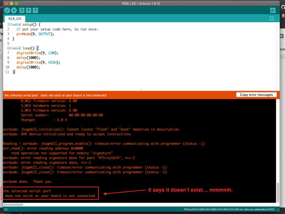
I had 110Ω between VCC and the board and got rid of it and it worked. Maybe it wasn’t 110Ω but 110,000,000,000,000Ω… ?
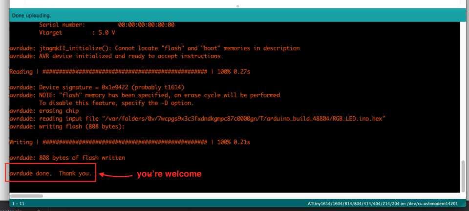
Now I have a nice message saying it’s all good, but my LED isn’t blinking… still, progress.
I tried with pinMode(9, INPUT); as it’s supposed to act as ground, but it doesn’t seem to work still.
Maybe I can try and read on the multimeter to see if there’s voltage going through? I checked and it does go up and down which means the programming works… but the LED does not? I can only detect the changes when I’m using the multimeter in DC V at 200m… and it only goes from 0.0mV to 2.3mV…
What does that mean? If I touch VCC to GND it reads 5V, the current goes through, or, the state is HIGH. If I touch VCC to nothing it shows 0V obviously, it has nowhere to go. If I touch VCC to PA1 it shows me 2.3mV, which is very close to 0V… is the LED actually a common cathode and not common anode? It stops current going the other direction, but still a tiny bit is going through?
Nope, I double-checked our components and it is a common anode.
I think I found the problem! I soldered the LED the wrong way. Where the triangle is in the corner, next to pin 1, should be where pin 3 is. Well, to be more precise, pin 1 (common anode) should be where pin 4 is.
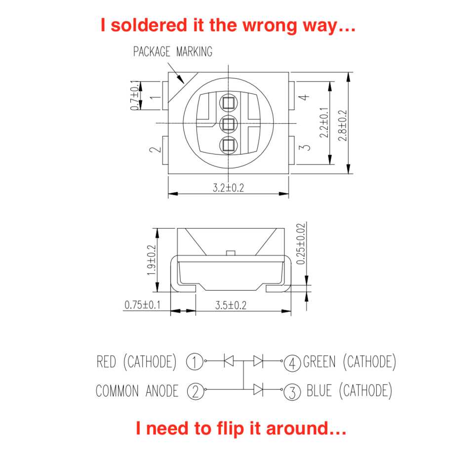
It works! Perfect. Assignment done.
... Na, let’s play a bit more, let’s make it what it is supposed to be, if a button is pressed the according color lights up.
int greenLed = 10;
int redLed = 9;
int blueLed = 8;
int greenButton = 0;
int redButton = 1;
int blueButton = 2;

void setup() {
  pinMode(redLed, OUTPUT);
  pinMode(greenLed, OUTPUT);
  pinMode(blueLed, OUTPUT);
  pinMode(greenButton, INPUT);
  pinMode(redButton, INPUT);
  pinMode(blueButton, INPUT);
}

void loop() {
  digitalWrite(greenLed, HIGH);
  digitalWrite(redLed, HIGH);
  digitalWrite(blueLed, HIGH);

  if (digitalRead(greenButton) == LOW) {
    digitalWrite(greenLed, LOW);
  } else {
    digitalWrite(greenLed, HIGH);
  }

  if (digitalRead(blueButton) == LOW) {
    digitalWrite(blueLed, LOW);
  } else {
    digitalWrite(blueLed, HIGH);
  }

  if (digitalRead(redButton) == LOW) {
    digitalWrite(redLed, LOW);
  } else {
    digitalWrite(redLed, HIGH);
  }

  delay(100);
}
Now we are done! Very nice.