
4.
Electronics Production
Assignments
group project:
characterize the design rules for your PCB production process
individual project:
make an in-circuit programmer by milling and stuffing the PCB,
test it, then optionally try other PCB processes
Download the files
This week there isn't much to download, but I attached the .rml files generated from mods, as well as the black and white PNGs to generate them.
Download RML filesTable of contents
Group assignment
Link to the group assignment on Tue's website
Testing the precision of milling
For our group assignment we milled a PCB board using the image below. It has a pixel density of 5000 dpi (dots per inch), which allows amazing precision when cutting.
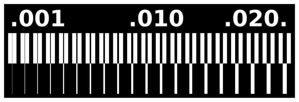
That is, if the machine can mill to great precision as well, hence the group test. The smallest end-mill we use is 1/64” (0.015 of an inch or 0.39mm).
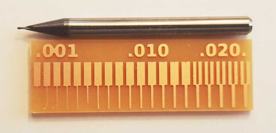
This is reflected in the image above, where you can see the cut failing halfway between 0.010 and 0.020.
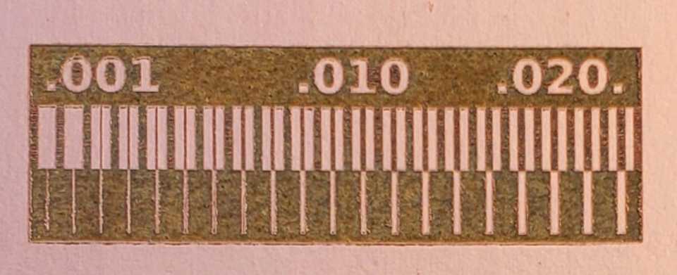
Fiber lasers have greater accuracy, almost cutting down to 0.001 of an inch.
Individual assignment
For this assignment I’m making the FabISP board. In the Fab Lab Barcelona we are 13 to do Fab Academy and decided that we’d all build a board needed during the program.
I didn’t know anything about the boards and decided to make the FabISP because of it’s name.
Here’s a link explaining in depth why the board is designed this way and which component does what. Very interesting read.
Preparing the .RML file
No need for documentation, I simply followed this tutorial, and made some adjustments.
By default the X, Y and Z axis have an offset value for their origin in the Roland SRM-20 milling machine module.
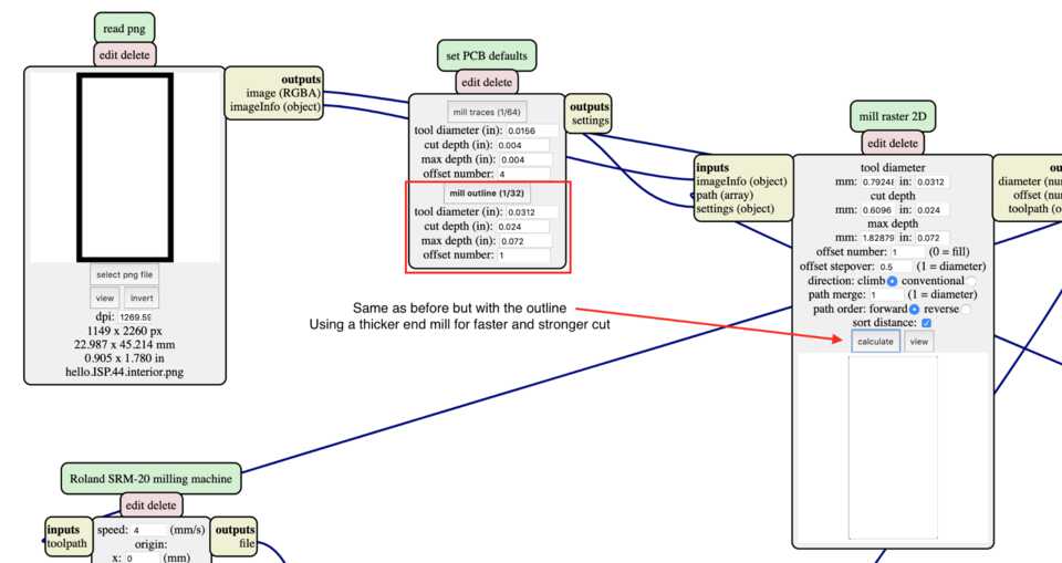
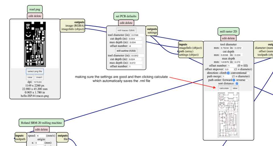
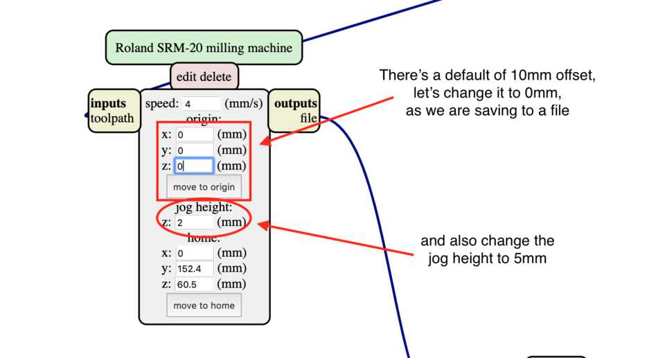
I realised this when I launched the milling and it was spinning a few mm above the PCB board.
I went back to the Mods and changed the origin to 0, 0, 0.
Milling the PCB
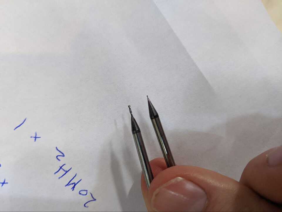
Below is a picture of the 1/32” and 1/64” end-mills. The thinnest one, 1/64”, is used to mill outside the traces. It has a higher resolution so that it can mill thin lines in between the traces to go to the ATtiny44.
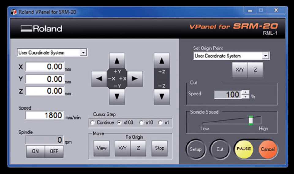
Before any milling you need to insert the appropriate end-mill for the task, and set the X/Y axis as well as the Z axis.
To do so, insert the tool, make sure it is tightly screwed so that it doesn’t lower as you mill. Move the tool so that it is a safe amount above the PCB board (something like 50mm), and move with Continuous mode towards the origin point of your board (which you decide, but usually further bottom-left possible). When you get near it, you change the Cursor Step to x100, x10 and x1 respectively.
Changing the speed mode is most important when lowering the tool on the Z-axis, so that it doesn’t crash into the board and possibly break this fragile end-mills.
Lower the end-mill slowly until it touches, or almost does, the board. Unscrew the end-mill and let it rest on the board, pressing on the board a tiiiny bit while screwing back on the end-mill. This means the end mill will be slightly pressing on the board.
Click on the ON under the Spindle menu on the left after having set the Cut Speed at 40% to check that the Z is at the right depth. It should create a tiny bit of dust.
If you are happy with it, press Set Z.
Doing the traces
After having set the X/Y & Z origins, reset the Cut Speed to 100% and having inserted the 1/64” end-mill, click on Cut, make sure to select the right file and click Output to launch the milling process.
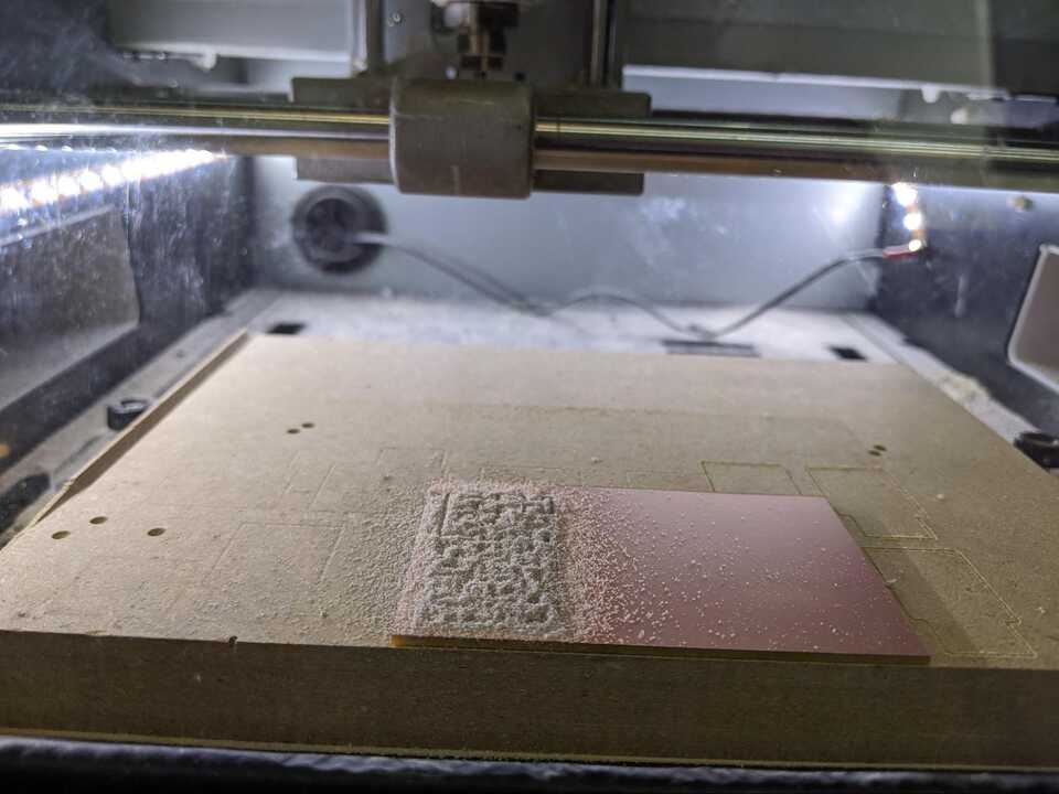
Done.
Doing the outline / interior
A little problem occurred on this step.
As we were doing the outline, I changed the end-mill to the 1/32” one. That means resetting the Z. I made sure the tool was up from the board and clicked Move to X/Y, and then slowly lowered the tool. I placed my Z, unscrewed the tool a bit and made sure it was resting on the PCB board. Screwed it back up nicely and made it spin to see if it created a little bit of dust. It did, nice! I clicked View to bring the board closer to do a final check that it’s all good. Yep, all good, let’s do this.
Ok, let’s get the file up, Cut > Add > hello.ISP.44.interior.png.rml and click Output. The tool is going down, and… wait what?! That’s way too deep! Pause!
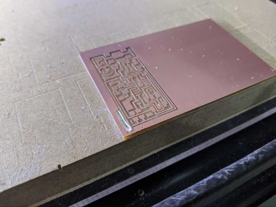
What happened?
Ah… I moved the tool to Z, but forgot to press the Set Z button. Damn. The tool broke. Game over, try again.
Same steps as before but make sure to press the Set Z button. Ok, it’s working now. Luckily it didn’t destroy the traces and the board was left intact. Phew.
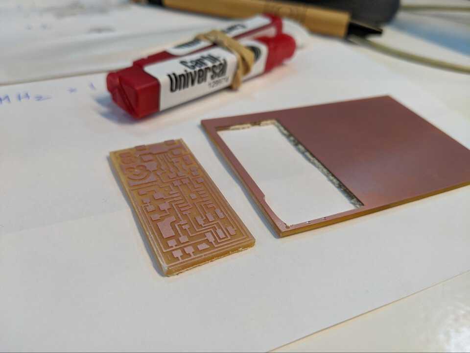
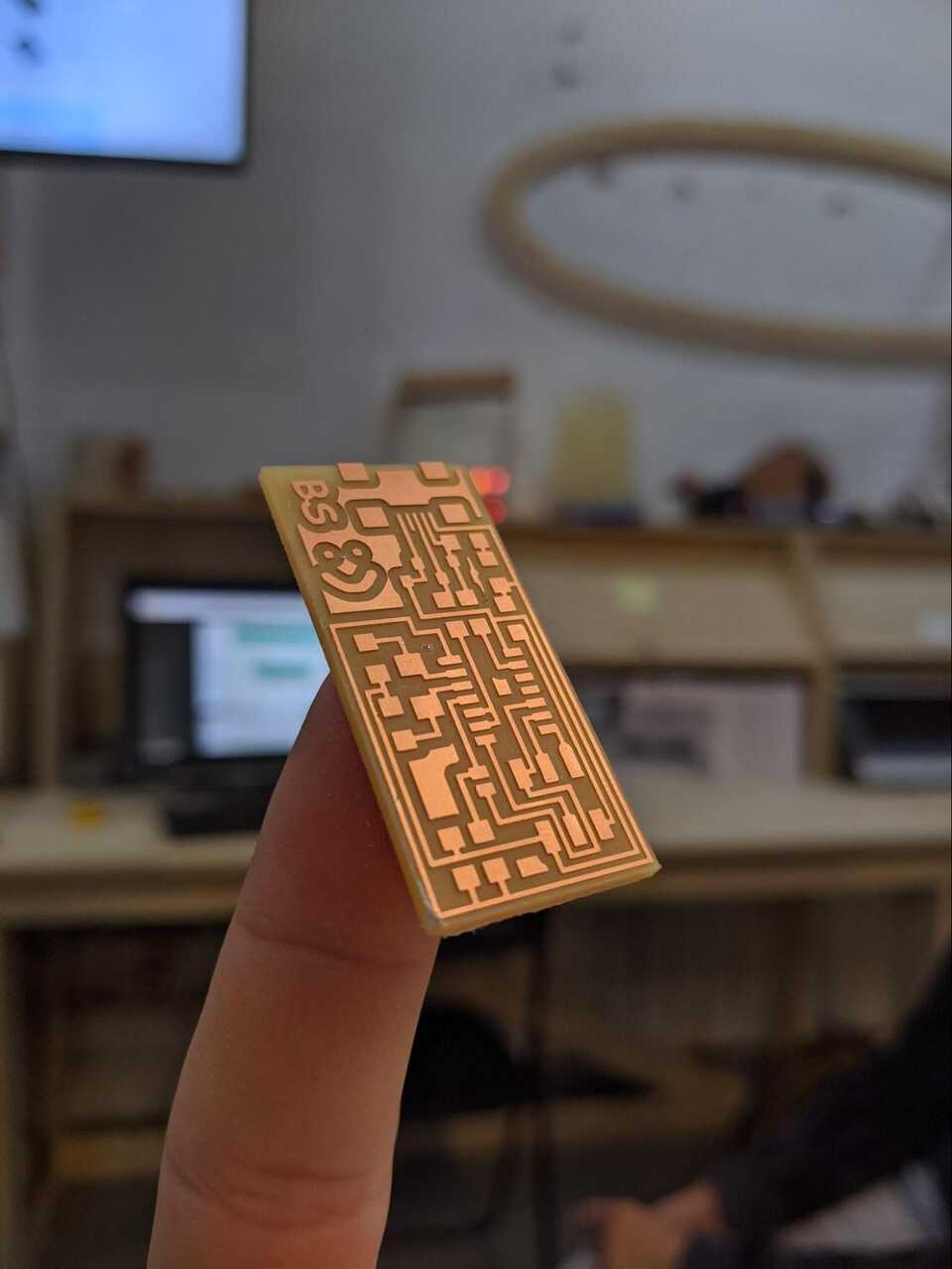
Done and undusted (hehe)
Soldering the PCB
The shopping list
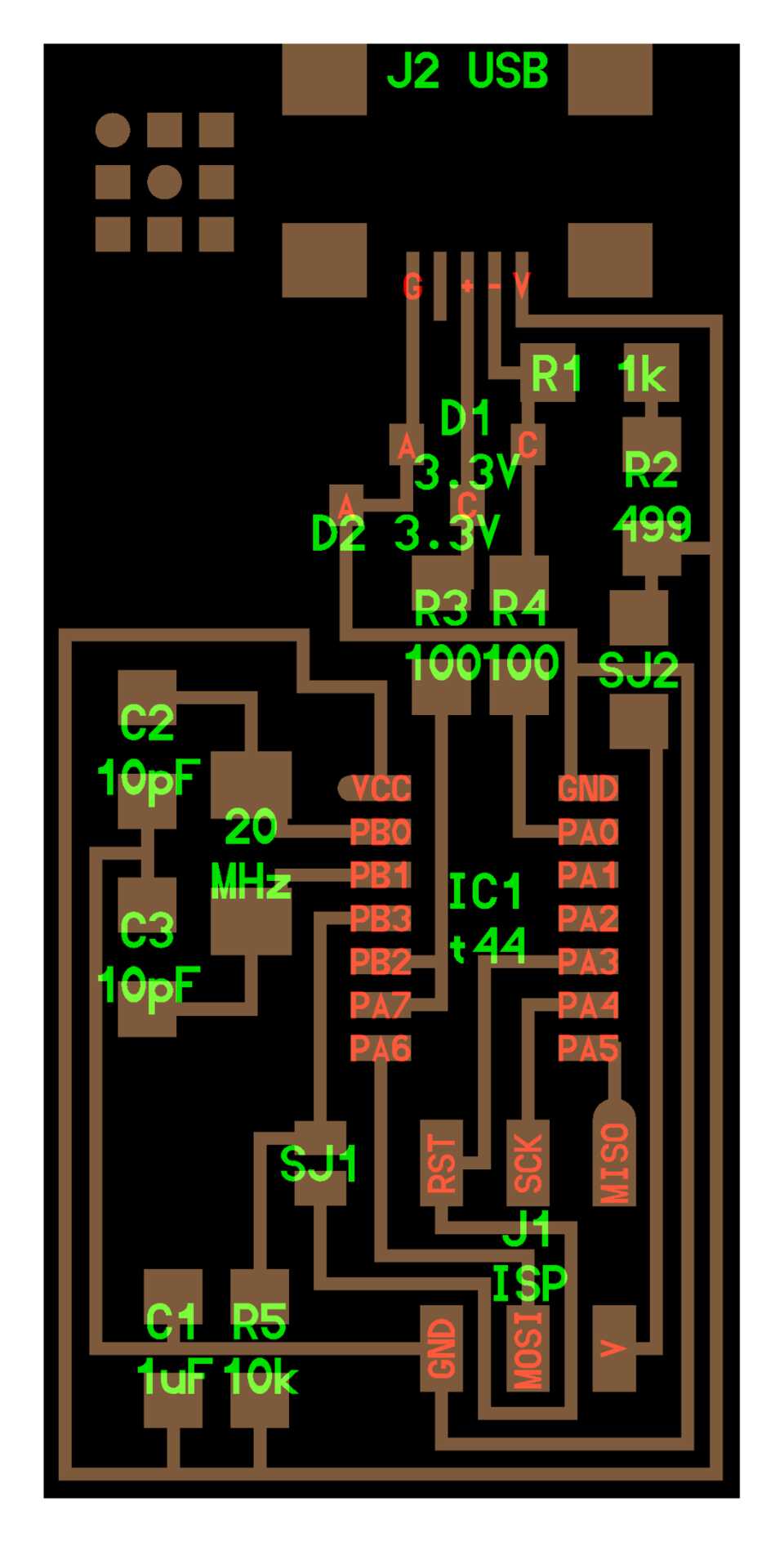
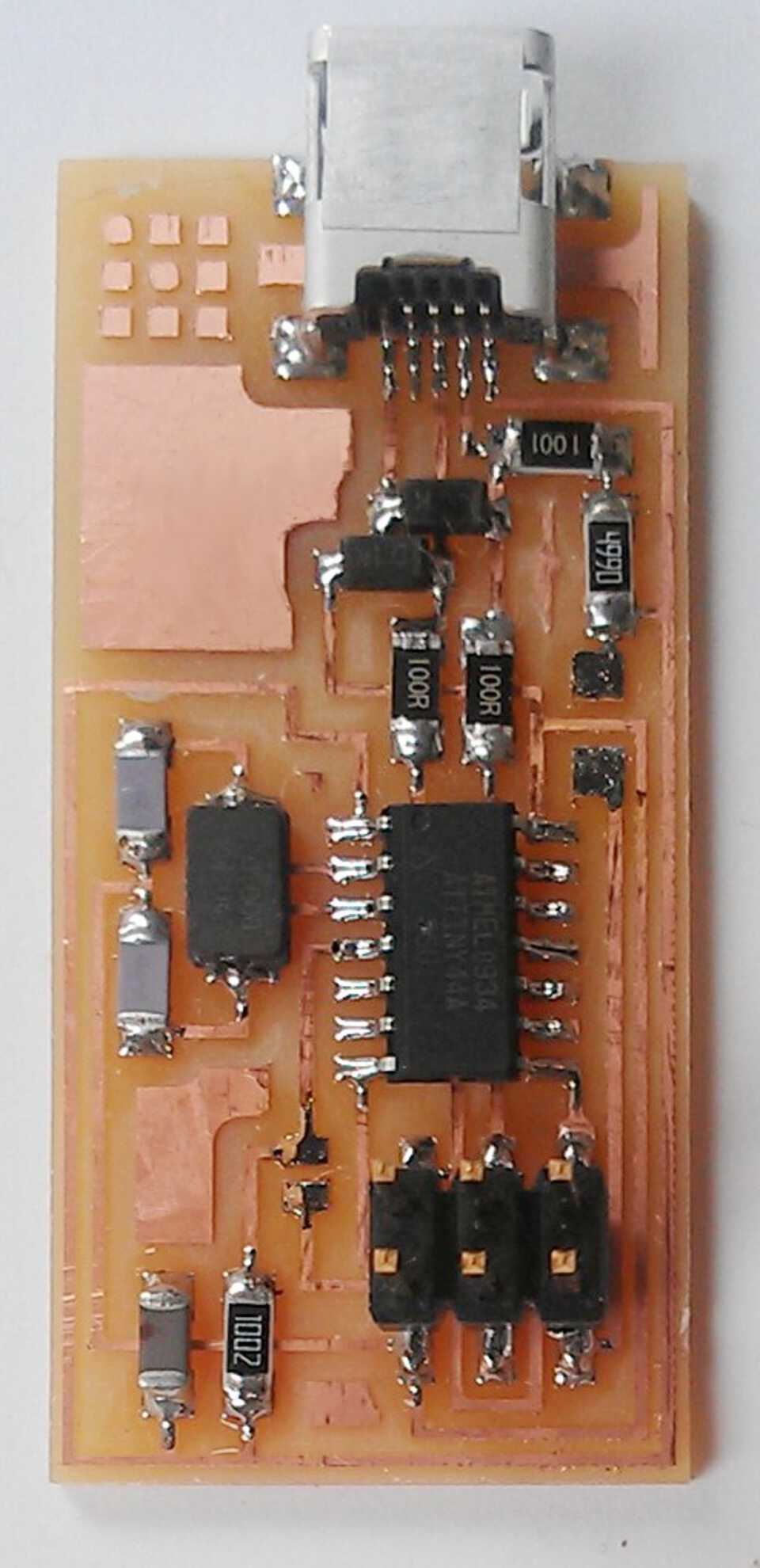
Above the board with the components
I’m writing down all the components we need, in the case of the FabISP they are:
- J2 USB
- R1 1K
- D1 3.3V
- D2 3.3V
- R2 499
- R3 100
- R4 100
- SJ2
- C2 10pF
- 20MHz
- C3 10pF
- IC1 t44
- SJ1
- C1 1uF
- R5 10k
- J1 ISP
Let’s go through them and check what they are and group them in families.
The Rs are resistors, measured in Ohms (Ω).
Resistors are electronic components which have a specific, never-changing electrical resistance. The resistor's resistance limits the flow of electrons through a circuit.
They are passive components, meaning they only consume power (and can't generate it). Resistors are usually added to circuits where they complement active components like op-amps, microcontrollers, and other integrated circuits. Commonly resistors are used to limit current, divide voltages, and pull-up I/O lines.
We need one 1kΩ, one 499Ω, two 100Ω and one 10kΩ.
The SJs, a.k.a jumpers, which connects different parts of the circuits together, jumping over a trace. They are simply resistors with no resistance (0Ω) which you then detach after initialising the FabISP for the first time.
We need 2 jumpers.
The Ds are diodes.
A diode is an electrical device allowing current to move through it in one direction with far greater ease than in the other.
We need two 3.3v diodes.
The Js are input and output connectors.
We need a miniUSB and 6 pins ISP.
The Cs are capacitors, measured in Farads.
What makes capacitors special is their ability to store energy; they're like a fully charged electric battery. Common applications include local energy storage, voltage spike suppression, and complex signal filtering.
The standard unit of capacitance is the farad, abbreviated. This is a large unit; more common units are the microfarad, abbreviated µF (1 µF =10-6F) and the picofarad, abbreviated pF (1 pF = 10-12 F).
We need one 1uF and two 10pF.
20MHz which is a resonator.
We need one 20MHz resonator.
IC1 is the chip, in this case t44 stands for ATtiny 44.
We need one of ATtiny 44.
Let’s grab them from the shelves. They are nicely organised with the amount of units from left to right, top to bottom, i.e. the jumpers are in the resistors section at the top left, but the 10k resistor is further down on the right.
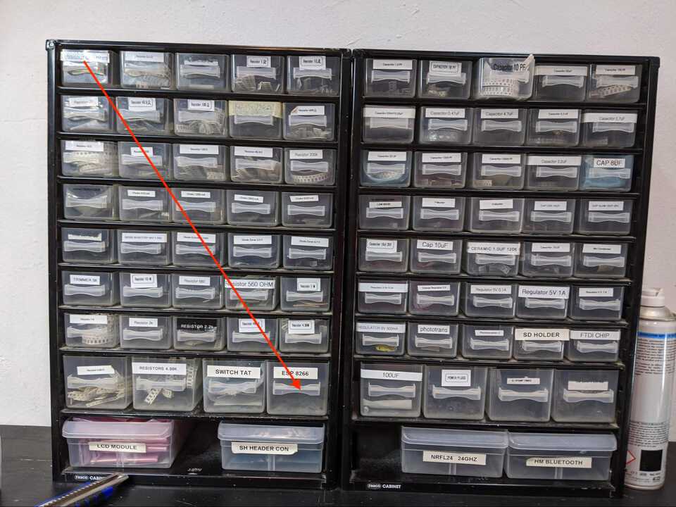
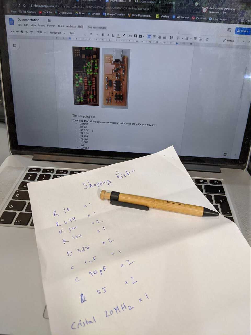
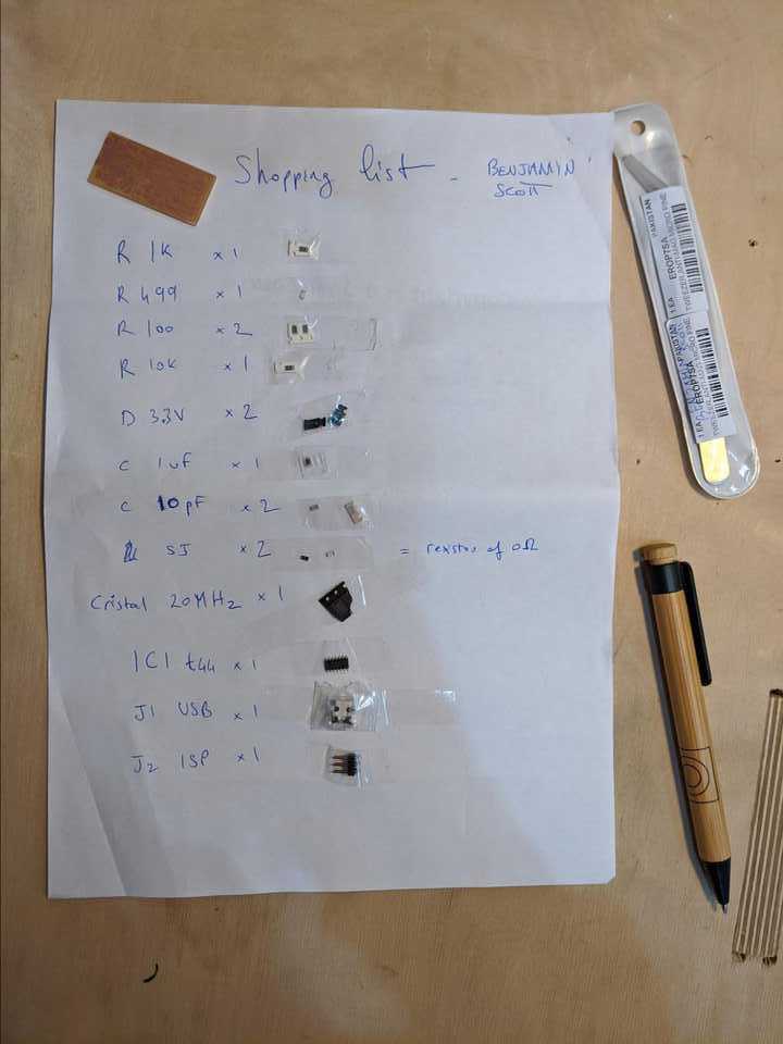
Finished shopping list. Xmas came late.
Order of the components to solder
Although we were told to do small-to-big and inside-to-outside, for this board Edu recommended that I start with the USB port as it’s quite intricate, and then the components just next to it.
Later I go for the chip in the middle of the PCB, and finish with the ISP connector.
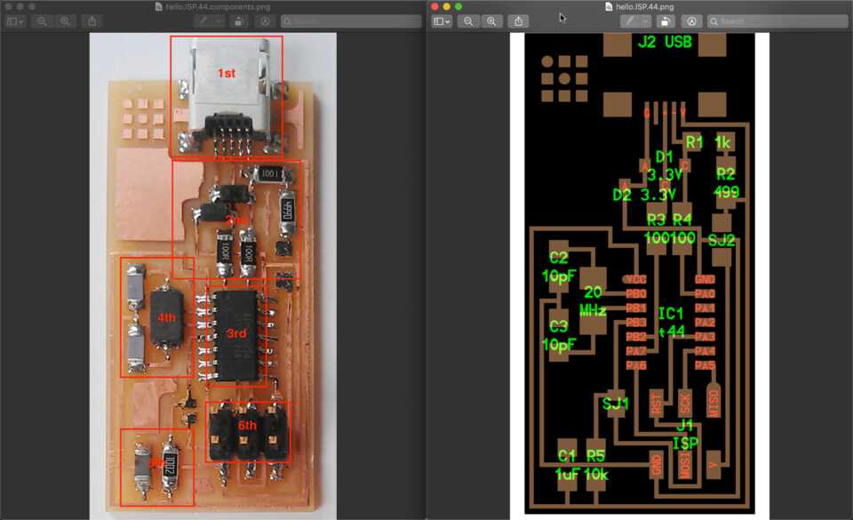
Soldering steps
Make sure you have everything you need with you, components, wet sponge, the soldering station, tweezers and a light source.
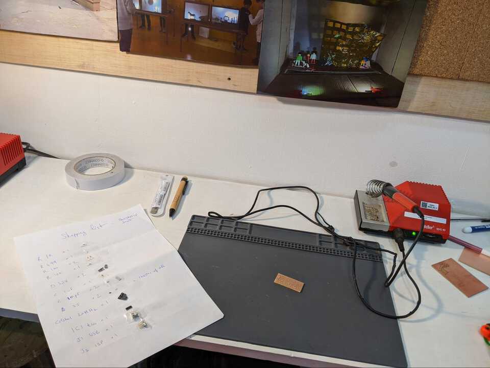
Missing above, the wet sponge. I was too hasty to document my work.
To solder it is essential to have a clean iron. Make sure you have a wet sponge to clean it from time to time. When you touch the sponge it cools down the iron. Wait a few seconds for it to heat up again before continuing your soldering.
In general, when soldering, touch the trace on the board for a few seconds with the iron to heat it up. It will help the lead spread evenly on the surface when you make contact with it.
Note //My friend Marco had a super nice macro lens you can put on top of your phone, which was amazing to take pictures during the soldering process. Obviously I couldn’t actually take pictures while soldering as you need both hands.
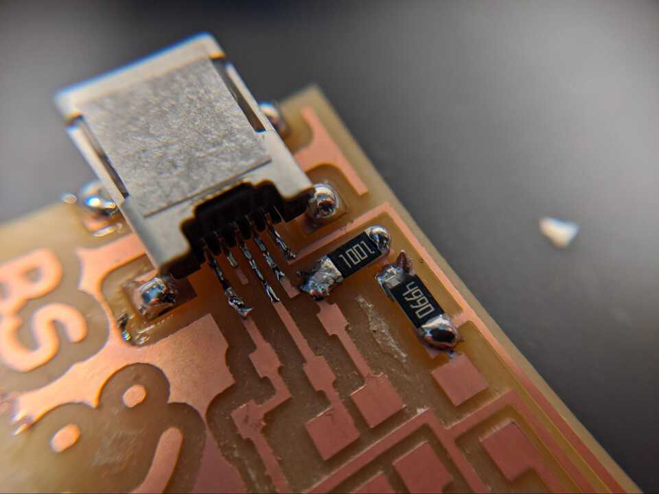
First components placed… exciting.
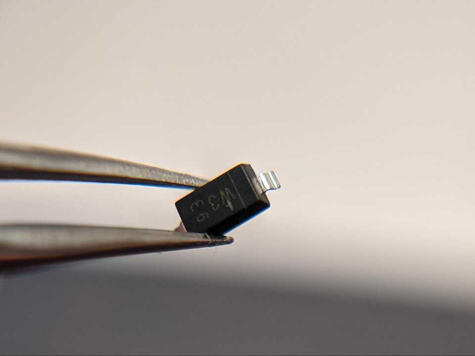
Here you can see the 3.3v diode and the line on the right which tells you the orientation to place on the circuit. It needs to be on the cathode side (the C on the diagram).
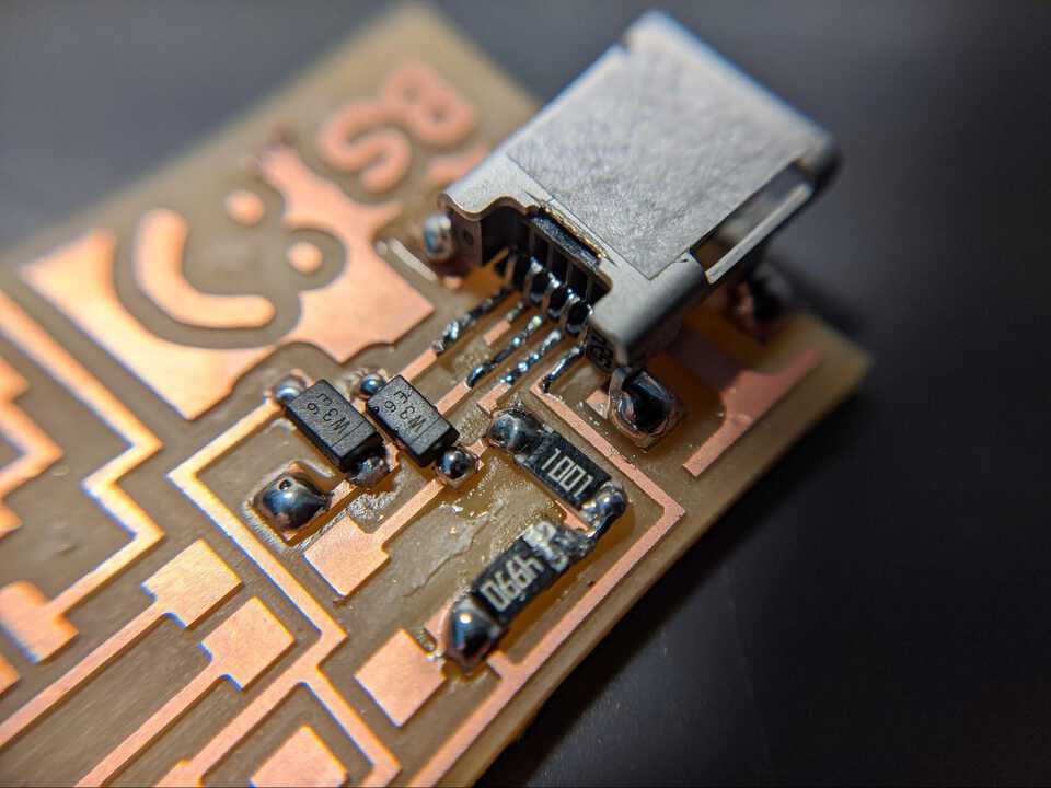
Here you can see the two diodes soldered on, and a drop of lead on the board to await for the resistor. You melt it and then place the resistor on top.
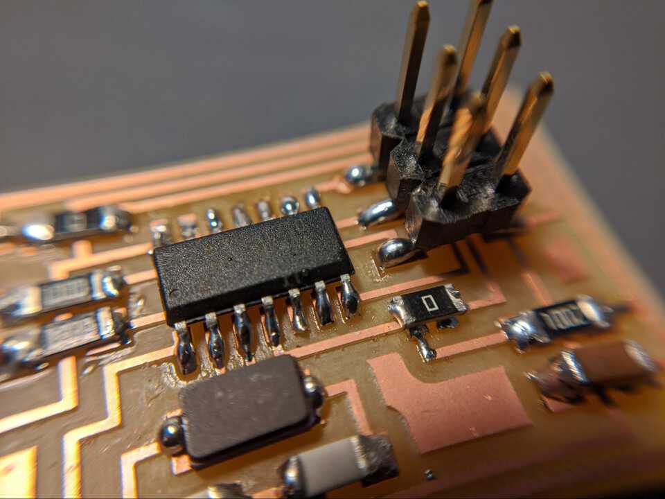
Finished board, I’m quite happy with it. Mostly shiny and clean around the ATtiny44.
Verifying the continuity and for shorts
At the end of it I used a multimeter to verify the continuity of the PCB board. I checked that there was no shortage between each pin of the ISP, of the ATtiny44 and then that there WAS continuity between the GND pins on the boards.
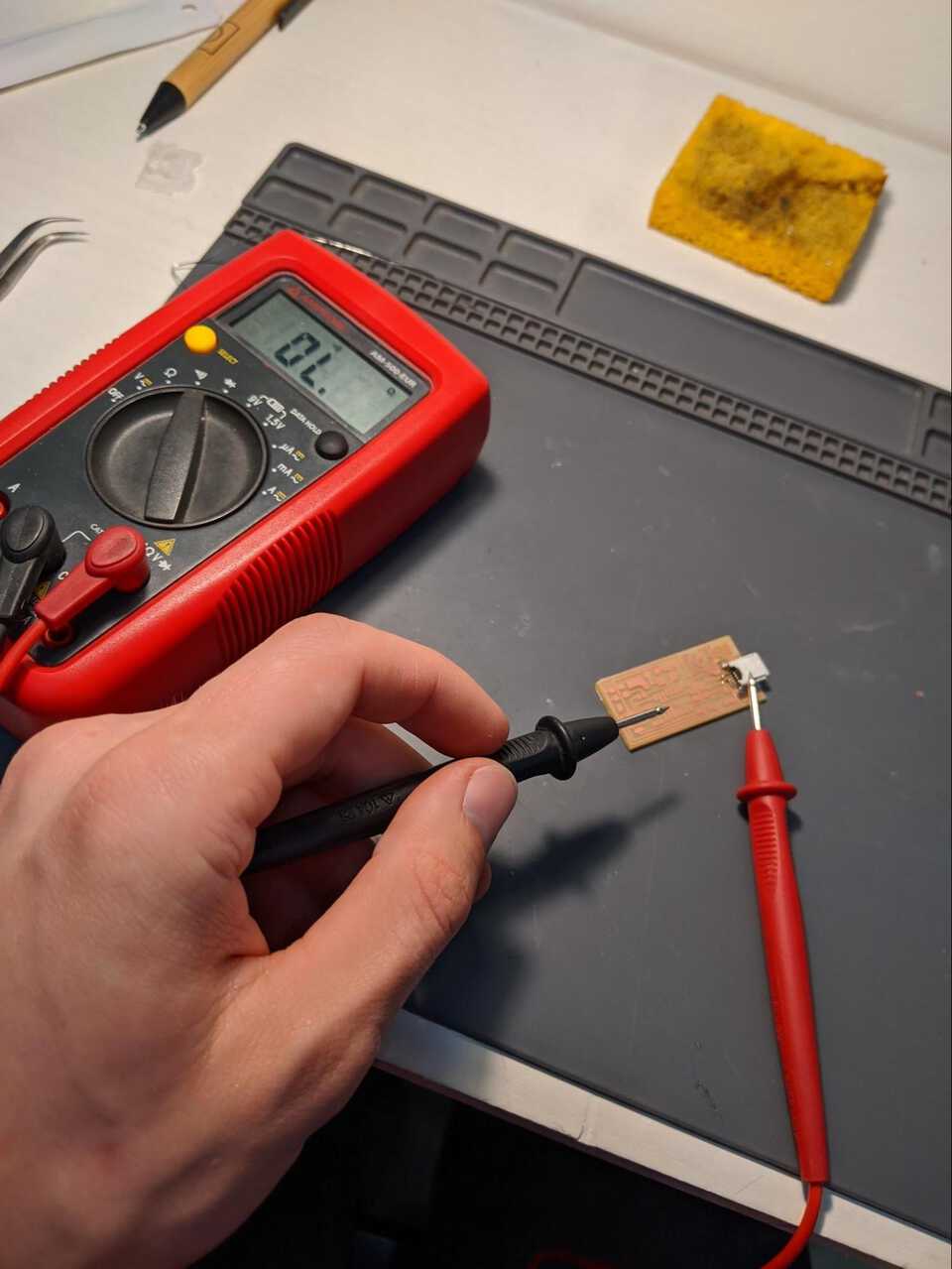
Multimeter in beep-beep mode.
Programming the board
To flash the board I used the AVRisp Mkii. I connected it to my computer, and then powered the FabISP through a separate power source (another USB plug).
Installing packages and downloading the FabISP firmware
I followed this tutorial, posted on the Fab Academy Schedule.
I installed the Crosspack AVR package as requested, and already had Make installed from previous Xcode projects.
I downloaded the FabISP Firmware for MacOS 10.8.2, unzipped it and then in the terminal moved into the directory.
Preparing the files to flash the board
I opened the Makefile with nano Makefile and then checked if it was all in order. It was.
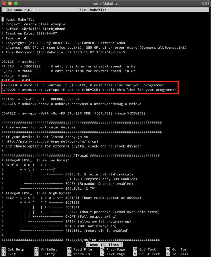
Then I executed the code in the tutorial, making the hex file.
$ make hex
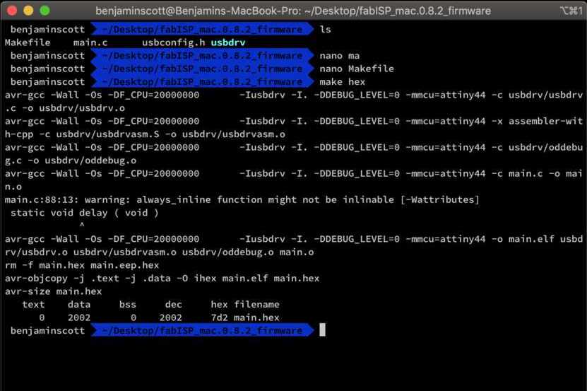
Everything’s fine so far. Next $ make fuse.

But here there’s an error...avrdude: usbdev_open(): did not find any USB device "usb"
Some Google research gives a few pages (1) (2) (3) to check, but nothing that seems to fix it for me.
In the end we tried the same steps on a Windows computer, and it all worked fine… Ok, mystery continues.
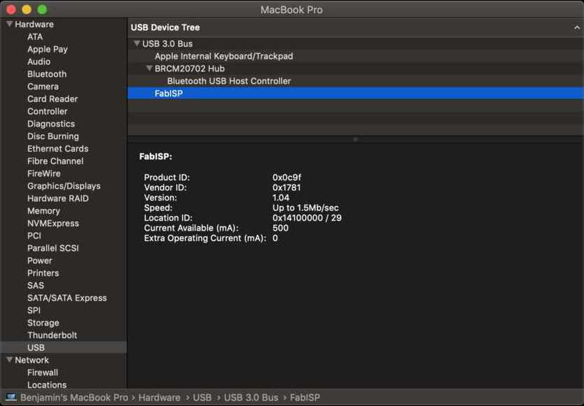
After programming it I plugged it to my Macbook, and in System Report is shows as FabISP.
Unsoldering the jumpers
Once the board is programmed, you have to unsolder the jumpers. One of the jumpers tells the board to be in “programmable” mode, while the other allows the FabISP to power the board it programs.
The only thing is, it provides 5V, and if you are programming a 3.3V board, you might fry it.
The solution is to unsolder both jumpers, and in the future power both boards when you want to program.
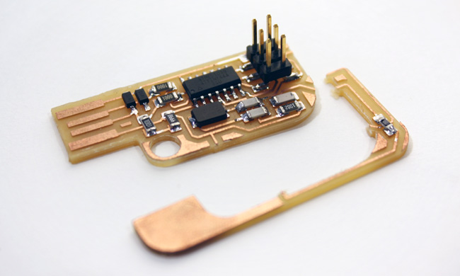
Edit: I really like what this guy did. He make the jumpers on the side of the board so you can break it after. It's genius!
Conclusion
I really enjoyed the soldering of the board. It was relaxing and meditative.
The board I soldered was the FabISP. I managed to flash it but didn't actually use it to program any other boards, yet.