EMBEDDED PROGRAMMING
So its complete lockdown announced by the government in Noida at the start of the week and its complete lockdwon in the country.
This week we have to read a data sheet and understand its different parts and program your board to do something with as many different programming languages and programming environments as possible and in the group assignment we have to compare the performance and development workflows for other architectures.
DATASHEET ATTINY 44
After working in the electronic production and design week on ATTNINY 44, i was not able to gather much knowledge about the working of the Microcontroller. There were pins and all the functionjs assigned to it was not that much clear. This week it is all about this. we have to read the datasheet of the microcontroller and understand the things.
The first page of the datasheet specifies about the Micrcontroller. The microcontroller which in my case is ATTINY 44 has these specifications.
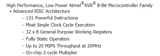
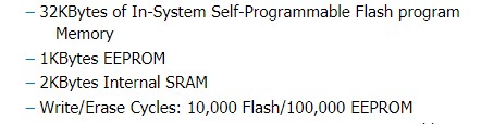
- It is a High performance, low power AVR® 8-bit microcontroller.
- 2/4/8K byte of in-system programmable program memory flash (Atmel® ATtiny24/44/84)
- 128/256/512 bytes in-system programmable EEPROM (Atmel ATtiny24/44/84)
- 128/256/512 bytes internal SRAM (Atmel ATtiny24/44/84)
- Programmable watchdog timer with separate on-chip oscillator
- 14-pin SOIC, 20-pin QFN/MLF: Twelve programmable I/O lines
- 2.7 - 5.5V for Atmel ATtiny24/44/84
- Atmel ATtiny24/44/84: 0 - 8MHz at 2.7 - 5.5V, 0 - 16MHz at 4.5 - 5.5V
- You need to create an account using this link
- Go to circuits as there are other options for simuation as well
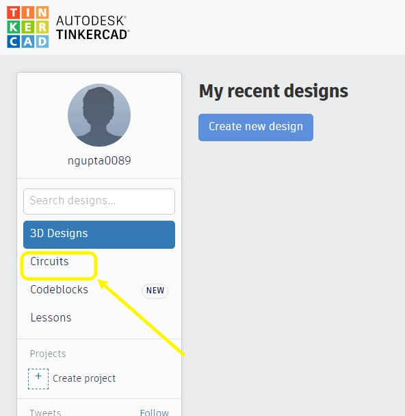
- From the dashboard you can select the components and code and simulation button as well
- • Arithmetic and logic unit
- • Control unit
- • Registers
- • Memory for data and instructions
- • Input/output interface
- • External storage functions
- CPU is unable to access program memory and data memory simultaneously.
- This case is called the "bottleneck" that affects system performance.
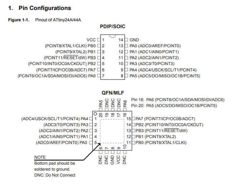
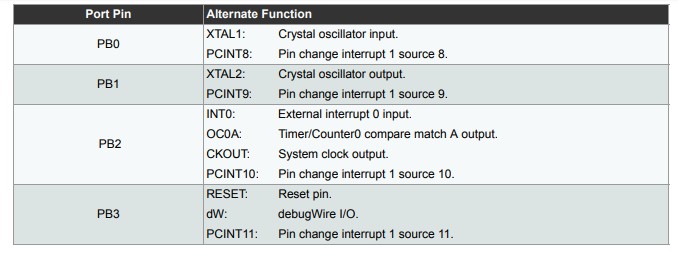
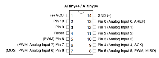
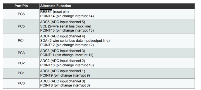
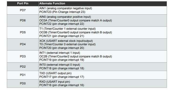
There are two images of the MC. The two images are of two different kinds of same microcontroller. The function of the pins are different and are specified in the datasheet itself. PA pins are for Analog to digital convertor pins. these pins also have other functions also but when there is an analog input then these pins should be used in the circuit.
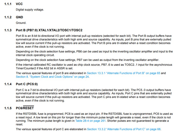
Pin description
VCC
Supply voltage.
GND
Ground.
Port B (PB3...PB0)
Port B is a 4-bit bi-directional I/O port with internal pull-up resistors (selected for each bit). The Port B output buffers have symmetrical drive characteristics with both high sink and source capability except PB3, which has the RESET capability. To use pin PB3 as an I/O pin instead of RESET pin, program (‘0’) RSTDISBL fuse. As inputs, Port B pins that are externally pulled low will source current if the pull-up resistors are activated. The Port B pins are tri-stated when a reset condition becomes active, even if the clock is not running.
RESET
Reset input. A low level on this pin for longer than the minimum pulse length will generate a reset, even if the clock is not Running.
Port A (PA7...PA0)
Port A is a 8-bit bi-directional I/O port with internal pull-up resistors (selected for each bit). The port A output buffers have symmetrical drive characteristics with both high sink and source capability. As inputs, Port A pins that are externally pulled low will source current if the pull-up resistors are activated. The port A pins are tri-stated when a reset condition becomes active, even if the clock is not running.
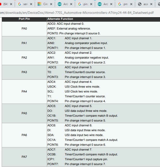
There are specicfic pins for the crystal or resonator but it doesnot mean that all other input devices cannot go inside it. If you want you can connect an led and program the MC.
The pins on the arduino board and the ATTINY board are different. So it is important that we know about the pin configurations.
Programming the board
This week i have to program the board with different programming languages. The board which we made in the week6 and with the help of the programmer which we made week 4.
But we do not have the lab access and the boards which we made are inside the lab so we found out another way to explore the programming language
Autodesk TinkerCad
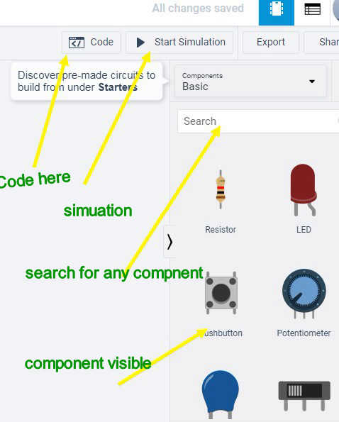
This software is very helpful for simulation and it provides simulation for 3D design and as well as circuits. I used this software to better my understanding about the working of the circuits becuase here you can experiment without the fear of any damage to the component as the components are virtual.
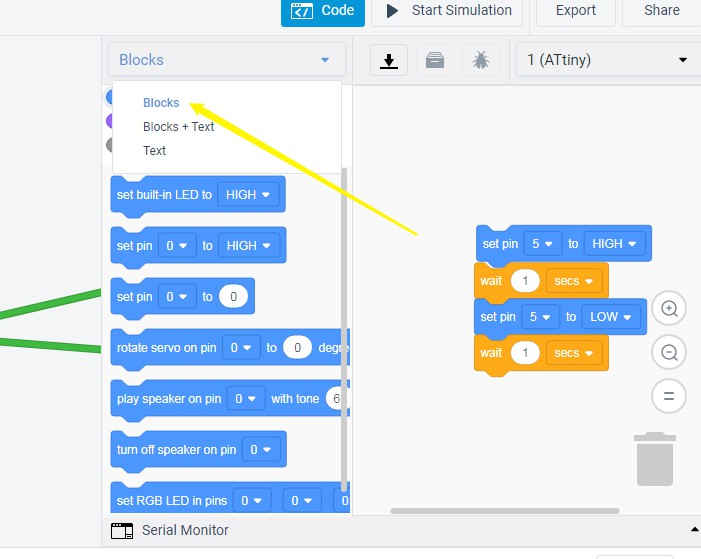
It gives you two ways to write a program (i) By using Blocks (ii) By using text
I found blocks to be easy as they are easily converted to text format and there you will not see any syntax error as the blocks do not reuire you to write the codes instead you need to slect the boxes. This videois helpful to learn about basic of TinkerCad.
I found it quite interesting so i started playing with it.
I made differnt circuits and programmed them
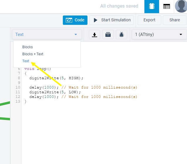
The circuit which i made was to program an ATTINY so that it makes the LED blinks with the use of the button
The components used in the simulation are 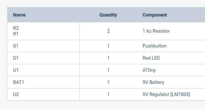
These are the some operating proceudre of Tnkercad
The process of operation is easy so here i got to experiment with the components more. I added components to the Attiny and progrmammed it.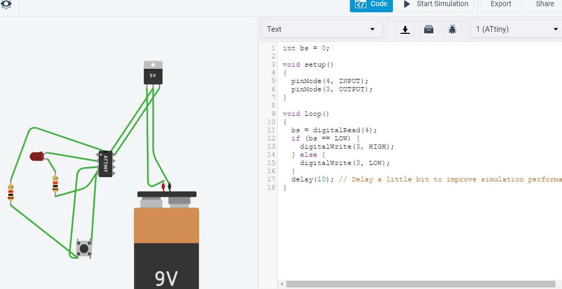
The code can be seen in the pic itself
ATMEGA 328
You can find the complete datasheet of Atmega328p through this link.
The information whcih a data sheet provides is very huge and cannot be read in a go and it is equally very difficult to understand that also.
So i am in my my project going to use three boards and i have programmed them. I am going to introduce you with steps of how to program ATmega328p Nodemcu and ESP32 Cam.
These videos helped me understand the process of programing Atmega328p and just to understand the mechanism i had used the throgh hole ic of atmegs328 and bought throughhole componets to test on the breadboard which was a good idea because that gave me confidence while programming the PCB of atmega328p.
Blink code using Fabtinyisp
The program is also uploaded by Fabtinyisp, we just need to change the programmer to usbtinyisp and just upload the code.
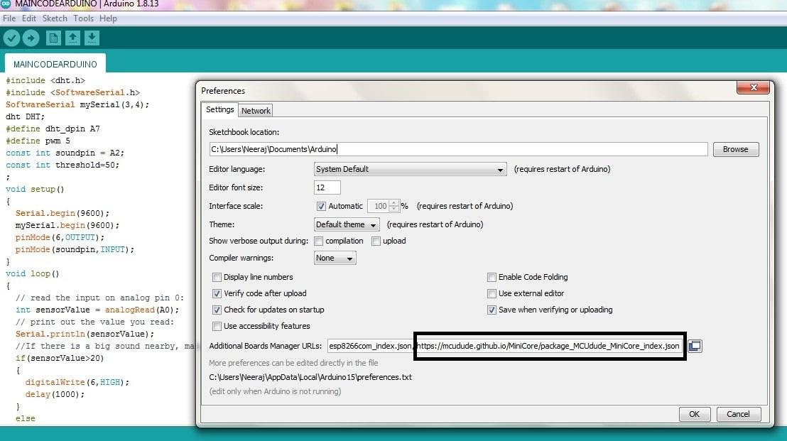
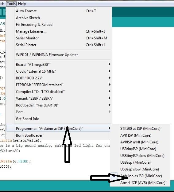
Steps to program the ATmega 328p
Step1:
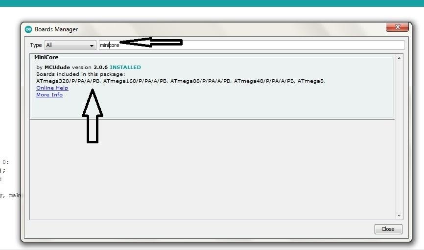
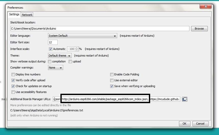
ATMEGA 328p requires the addition of a library known as MINICORE. You also need to add a line on the prefernece section of the Arduino IDE which you can get from .
Step2:After that you have to go to the board manager and fingd the minicore library and then you need to install the latest version.
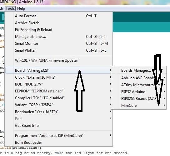
Step3:
Now you can see that in the boards section atmega 328 is visible and you can select that for programming.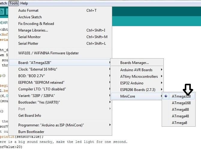
Step4:
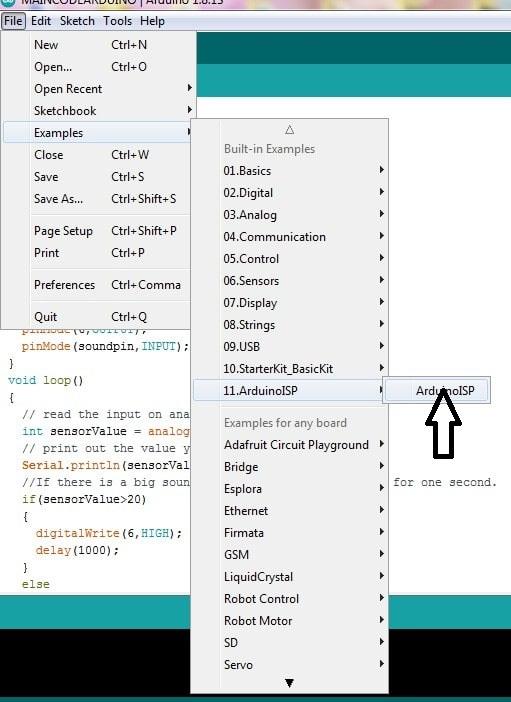
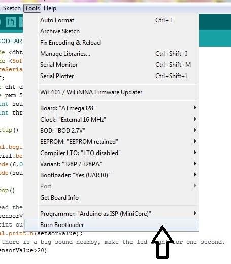
Burn the bootloader using arduino uno.
For this we need to first upload the program to arduino board for it to work as a programmer. The program can be found in the EXAMPLE setion of the arduino IDE. Just upload that program directly to the arduino board by selecting arduino uno from the board section. After that we can burn the bootlaoder to the chip.
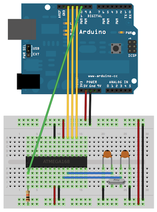
This is how the connections should be made to burn the bootloader. There are 6 pins which should be connected between the board and the arduino uno. These are MISO, MOSI, SCK, RESET, VCC AND GND. RESET pin of the ATMEGA328p should be connected to the pin 10 pf the arduinio uno. 13, 12 ,11 to the sck miso and mosi respectively.
It really becomes very frustrating to see that your board gives eror of certain types. Tha main cause of the error are:
1. The connections are wrong it means that you have not connected the pins rightly.
2. The soldering done on the board is not proper and you need to check your board with the help of multimeter.
3. While soldering your board must have become overheated and it is now burnt and there is a need to change it.
4. There is a short in your board and which is not letting it to program.
5. The volatge regulator which you have soldered has burnt off and which has led the higher volt supply to your microcontroller which will again fry the IC and there is a need to change it.
All the reasons which are listed above have happened with me and i have literaarly soldered many components again and again..
The video above shows the blink code which has been uploaded to the board after burning the bootloader.
NODEMCU
NodeMCU is an open source Lua based firmware for the ESP8266 WiFi SOC from Espressif and uses an on-module flash-based SPIFFS file system. NodeMCU is implemented in C and is layered on the Espressif NON-OS SDK.
The firmware was initially developed as is a companion project to the popular ESP8266-based NodeMCU development modules, but the project is now community-supported, and the firmware can now be run on any ESP module.
Programming NODEMCU
Programming NODEMCU with arduino IDE is not much different than programming other boards but the thing which should be remembeered is that there are some libraries which you need to download to use any board. So here i am going to explain you the step wise method to program the NODEMCU board with Arduno ide.
Step1: Write the prefernece for nodemcu which will let you to see it in the boards manager.
Step2: Download the library from the boards manager.
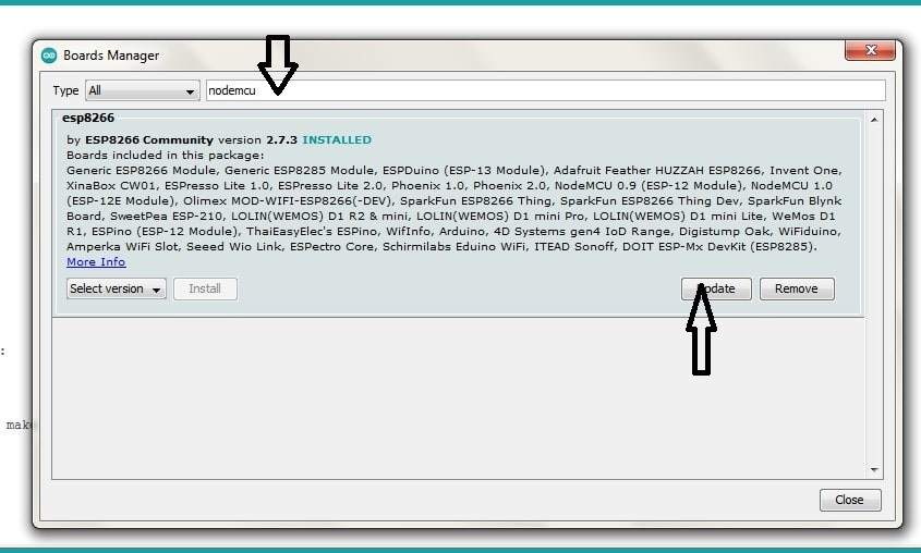
Step3: Nodemcu board will be visible in the tool section
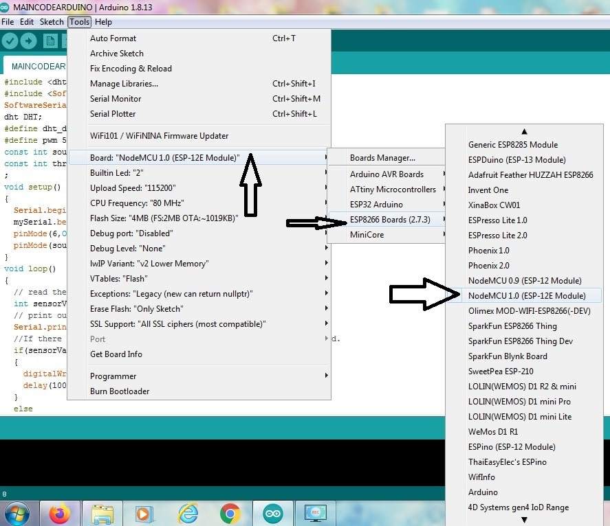
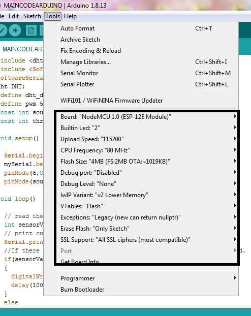
Step4: Set the process with which you want to proceed
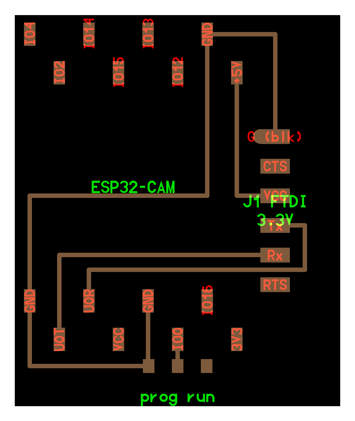
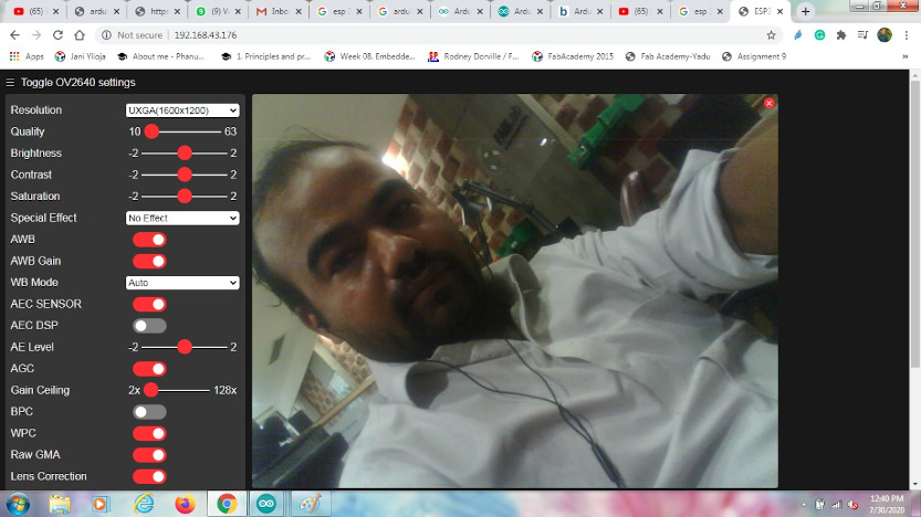
ESP32 CAM
I find this cam to be very easy to use and but its programmijgis a bit difficult because it does not have a programmer and there is no usb port ar anu other kind of port with which you can attach it.
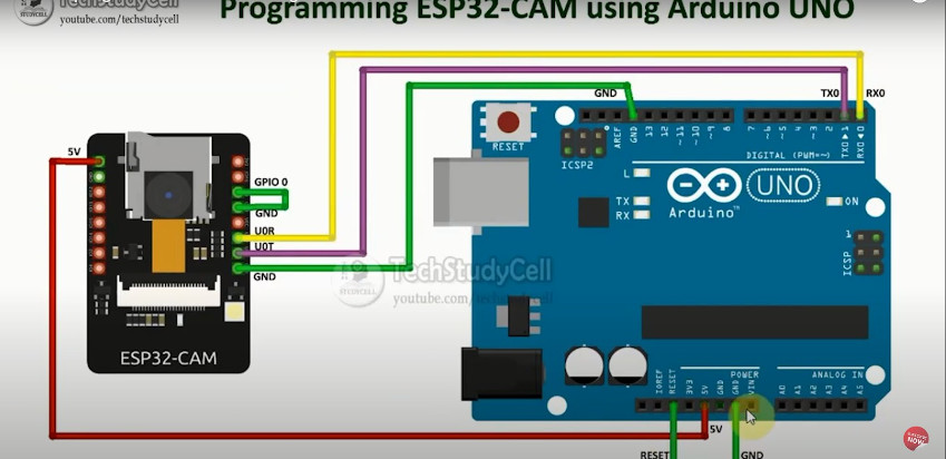
The fabacdemy page has a board for it as well. Prof Neil has expalined it well during his lecture on how to use this CAM model with the board. The difficulty in programming is that you need to remove the short between ground and GPIO 0 when you press the reset button to obtain the IP address for the live streanming.
The Board has a slide switch which is activated whenever any of the function is required.
This is the board which i soldered and used for the ESP 32 CAM
.jpg)
.jpg)
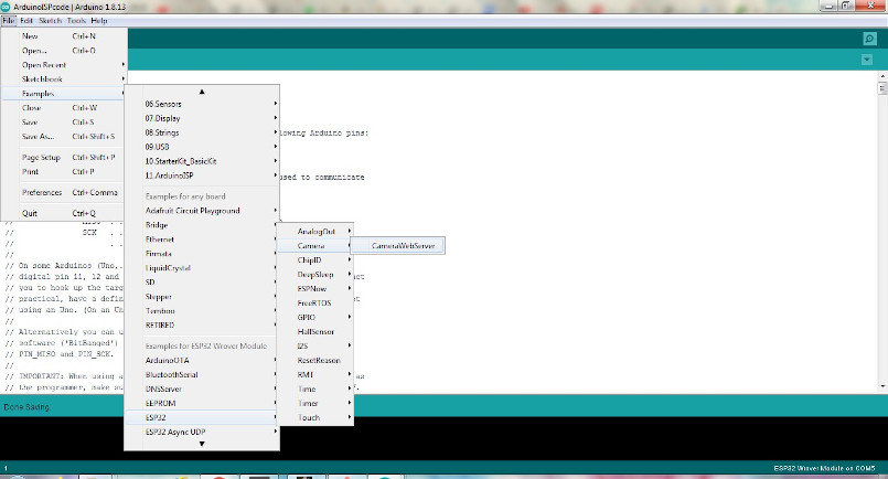
In the example section for the esp 32, there is a camera option and when you click it you wuill get the code of it. You need to make some modifications on it such as the wifi name and password and which board you are going to use. The esp32 boards are manufactured by different companies so you need to select the name of the company from the code itself (in my case it was tthinker).
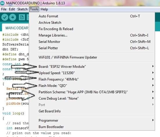
These settings should be there while uploading the code.
Download all code files
Programming using C
I also need to program my board with more languages so i am using C for programming my board. The process is simple. You neeed to write your code and use the Arduini IDE to upload the code. But the code in C is differnt and it reuires the knowledge of the language.
I have programmed my board with C to blink an LED.
The code is like this
            /*This work by NEERAJ GUPTA is licensed under a Creative Commons Attribution-ShareAlike 4.0 International License.*/

            #include "avr/io.h" //Import header file required for AVR microcontrollers
                #include "util/delay.h" //Import header flie required for delay function
                int main(void)
                {
            DDRA = 0b10000000; //set PA as output
                while (1) //Infinite Loop
                {
                PORTA |= (1<<3); // Set PA3 high (Make LED ON)
                    _delay_ms(1000); //delay of 5 sec
                        PORTA &= ~(1<<3); // Set PA3 low (Make LED OFF)
                            _delay_ms(1000); //delay of 5 sec
                                        }
                                                }
The program lets the led to blink for 1 sec and then remains off for one second. You need to import the header file required for AVR microcontroller and then inport the header file for the delay function. DDRA is used when using PA ports and DDRB to be used for PB ports. If using PB ports you need to write DDRB=0b111111111 and then you can move ahead whne programming with PB ports. Then there is a while loop which runs the fucntion again and again. PORTA is used and PORTB can also be used when using PB side. then delay for 1 second is provided in the code .
Using Python
I have learnt to program a Rasp Pi board which runs on Python. It was a new learning for me as till now we only had worked with arduino uno and other boards made by me. But this time i am doing something new.
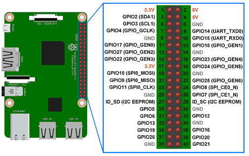
Rapberry Pi board is completely differnt than an arduino board. If you compare both of them, then arduino is like a calculator and Rasp pi is like a full fledged computer. It has its own CPU, 40 GPIO pins, audio jack , 4 USb ports and memory card slot and it is very powerful.
It works on python so i read something anbout the pythin programming. The code which i used for uploading on the Raspi board is
            /*This work by NEERAJ GUPTA is licensed under a Creative Commons Attribution-ShareAlike 4.0 International License.*/

            import RPi.GPIO as io // To import the RPi.GPIO module
            import time           // To import the time module
            io.setmode(io.BCM)     // Pin configuration selection
            io.setwarnings(False)    // warning if the code is not running due to alraedy existing program or else
            l=2   // Defining pin
            m=3   // Defining pin
            io.setup(l,io.OUT)   // Set the pin as output pin
            io.output(m,io.OUT)    // set the pin as putput pin
            while 1:              // while loop

                io.output(l,io.HIGH)     // set the pin as high
                io.output(m,io.LOW)         // set the pin as low
                time.sleep(2)               // wait for 2 seconds
                io.output(l,io.LOW)         // set the pin as low
                io.output(m,io.HIGH)            // set the pin as High
                time.sleep(1)                   // wait for one second
The python program has two leds at two Gpio pins. the program is blinking them. It is setting one led high for seconds and them setting the other high for 1 second.
For working on the python, you need to import the module as i have imported the RPi. GPIO module for raspberry pi board and time module aas well for setting up the time. the Pin configuration is by two types: One in thr form of pin numbers which are in sequence and the other in the foem of GPIO number. So if we are using the GPIO pin numbers in the program we have to setmode as BCM and if we are using the second type of pin confuguration Then we have to set the mode as BOARD. The code is expalined line by line in the code itself.
The pin configuration for the raspiberry pi is shoen in the image
So i had worked on arduino board but now i have also worked on Raspi board.
Group Assignment
Our assignment was to compare the performance and development workflows for other architectures
Architecture of a micro computer or a micro controller refers to the arrangement of the CPU with respect of the RAM and ROM. Hence, the Von-Neuman and Harvard architecture are the two ways through which the micro controller can have its arrangement of the CPU with RAM and ROM.
Computer Architecture refers to the internal design of a computer with its CPU, which includes:In a Von-Neumann architecture, the same memory and bus are used to store both data and instructions that run the program. Since you cannot access program memory and data memory simultaneously, the Von Neumann architecture is susceptible to bottlenecks and system performance is affected.
If a Von Neumann machine wants to perform an operation on some data in memory, it has to move the data across the bus into the CPU. When the computation is done, it needs to move outputs of the computation to memory across the same bus. The amount of data the bus can transfer at one time (speed and bandwidth) plays a large part in how fast the Von Neumann architecture can be. The throughput of a computer is related to how false the processors are as well as the rate of data transfer across the bus. The processor can be idle while waiting for a memory fetch, or it can perform something called speculative processing, based on what the processor might next need to do after the current computation is finished (once data is fetched and computations are performed).
The Von Neumann bottleneck occurs when data taken in or out of memory must wait while the current memory operation is completed. That is, if the processor just completed a computation and is ready to perform the next, it has to write the finished computation into memory (which occupies the bus) before it can fetch new data out of memory (which also uses the bus). The Von Neumann bottleneck has increased over time because processors have improved in speed while memory has not progressed as fast. Some techniques to reduce the impact of the bottleneck are to keep memory in cache to minimize data movement, hardware acceleration, and speculative execution. It is interesting to note that speculative execution is the conduit for one of the latest security flaws discovered by Google Project Zero, named Spectre.
Applications and features of Von Neumann Architecture
The Von Neuman architecture has got extensive application in everyday life. Keeping in mind the extensive application the Von Neuman architecture has been introduced as a subject in the engendering degree. From the third semester engineering students will have the subject as their curriculum. The Von Neuman architecture consists of some important features and here we will have a detailed elaboration to the features.
Harvard architecture:Harvard Architecture The Harvard architecture stores machine instructions and data in separate memory units that are connected by different busses. In this case, there are at least two memory address spaces to work with, so there is a memory register for machine instructions and another memory register for data. Computers designed with the Harvard architecture are able to run a program and access data independently, and therefore simultaneously. Harvard architecture has a strict separation between data and code. Thus, Harvard architecture is more complicated but separate pipelines remove the bottleneck that Von Neumann creates.
The main advantage:Computers designed with the Harvard architecture are able to run a program and access data independently, and therefore simultaneously.
Harvard architecture is more complicated but separate pipelines remove the bottleneck that Von-Neumann creates.
Applications and features of Harvard Architectures
The principal advantage of the pure Harvard architecture—simultaneous access to more than one memory system—has been reduced by modified Harvard processors using modern CPU cache systems. Relatively pure Harvard architecture machines are used mostly in applications where trade-offs, like the cost and power savings from omitting caches, outweigh the programming penalties from featuring distinct code and data address spaces. Digital signal processors (DSPs) generally execute small, highly optimized audio or video processing algorithms. They avoid caches because their behavior must be extremely reproducible. The difficulties of coping with multiple address spaces are of secondary concern to speed of execution. Consequently, some DSPs feature multiple data memories in distinct address spaces to facilitate SIMD and VLIW processing. Texas Instruments TMS320 C55x processors, for one example, feature multiple parallel data buses (two write, three read) and one instruction bus. Microcontrollers are characterized by having small amounts of program (flash memory) and data (SRAM) memory, and take advantage of the Harvard architecture to speed processing by concurrent instruction and data access. The separate storage means the program and data memories may feature different bit widths, for example using 16-bit wide instructions and 8-bit wide data. They also mean that instruction prefetch can be performed in parallel with other activities. Examples include the PIC by Microchip Technology, Inc. and the AVR by Atmel Corp (now part of Microchip Technology). The speed aspect : A lot has been discussed about the Harvard architecture, but without the speed any architecture can’t be accepted. But in case of the Havard architecture the manufacturers have designed the architecture in such a way that it will be able to process the data with a much higher speed. Yes, all care has been taken so that the architecture can process data with a high speed. By implementing the same formula the modern days CPU are being manufactured so that the new CPU can run with a much faster sped and can also process the data effectively. The concept of the CPU cache is also being implemented while designing the Harvard architecture.