ELECTRONIC DESIGN
This week we have to perform an electronic design assignment where it is required to recreate a hello echo board
with an addition of LED and a switch. We have to understand the basic of electronic equipments for which our
instructor Mr.Rahul Gautam gave an insight about the basic functions of the various equipments. We were also
introduced to the basics of the software from Autodesk Eagle. It can be easily downloaded from
this link.
This link
is very useful for understanding the basics of Eagle.
Since i am from mechanical engineering so it is going to be new to me to redisgn a board in Eagle.
The steps involved are:
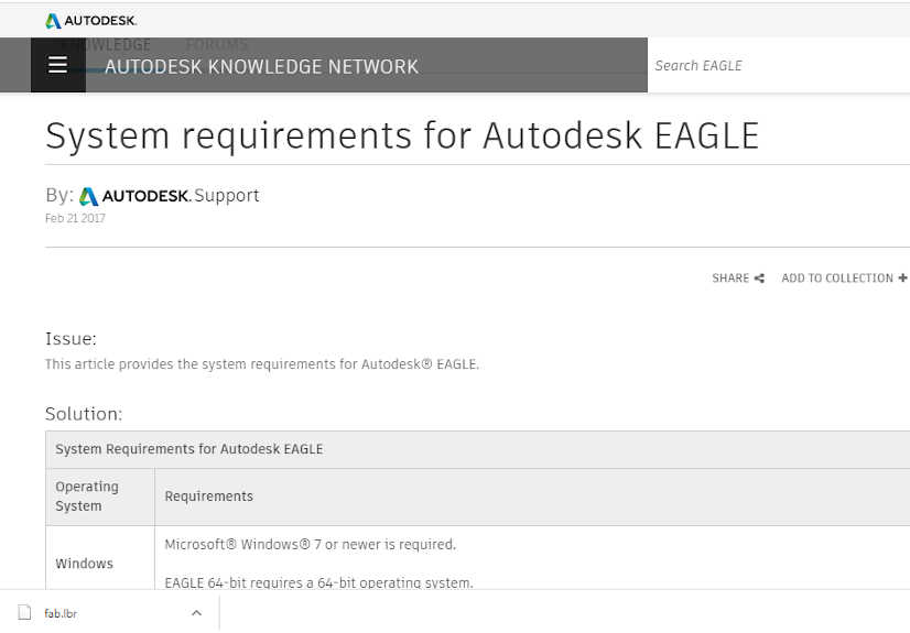
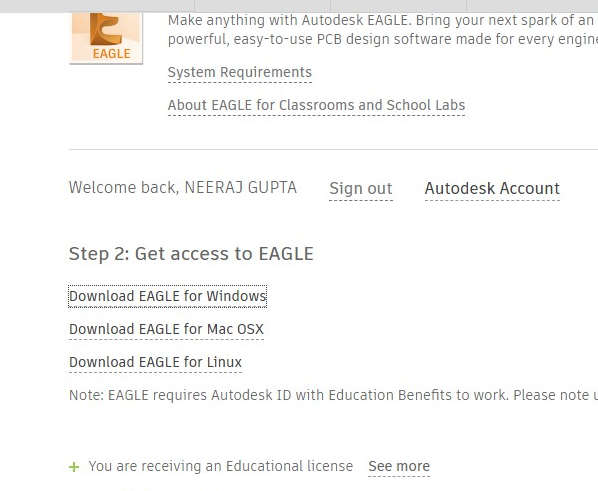
Download Eagle: Use this link
to download the software.
It will also specify the system requirements which should be there.
You need to click on new and then project.
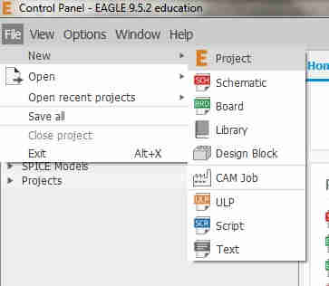
Under the new project you have to select a new schematic page on which you will put the components which are there to be added.
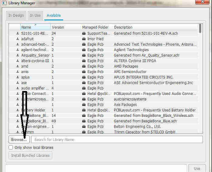
>There is a need to add library which consists of all the components of the same footprints so that the design coming out is optimised.
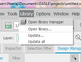
>The library is to be added to the set of libraries already present in the software. You need to go
to Library
and then to library Manager and then availaible and then you need to
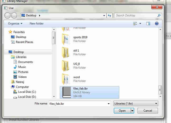
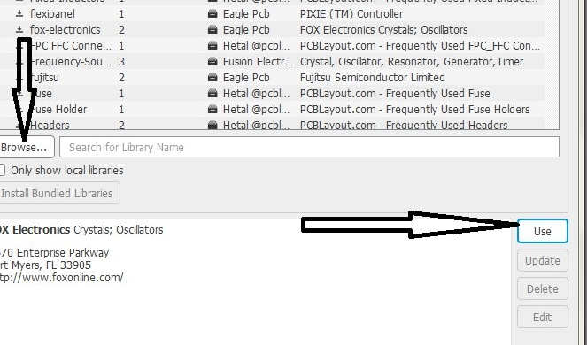
browse the required file
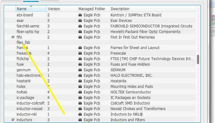
and then click on Use. the library will be added, the problem which i faced is i
have to repetaedly add the fab libraray whenever i was
starting a new project.
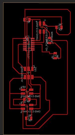
>I started with a design on a piece of paper where i took help from the class pages and came out with this design.
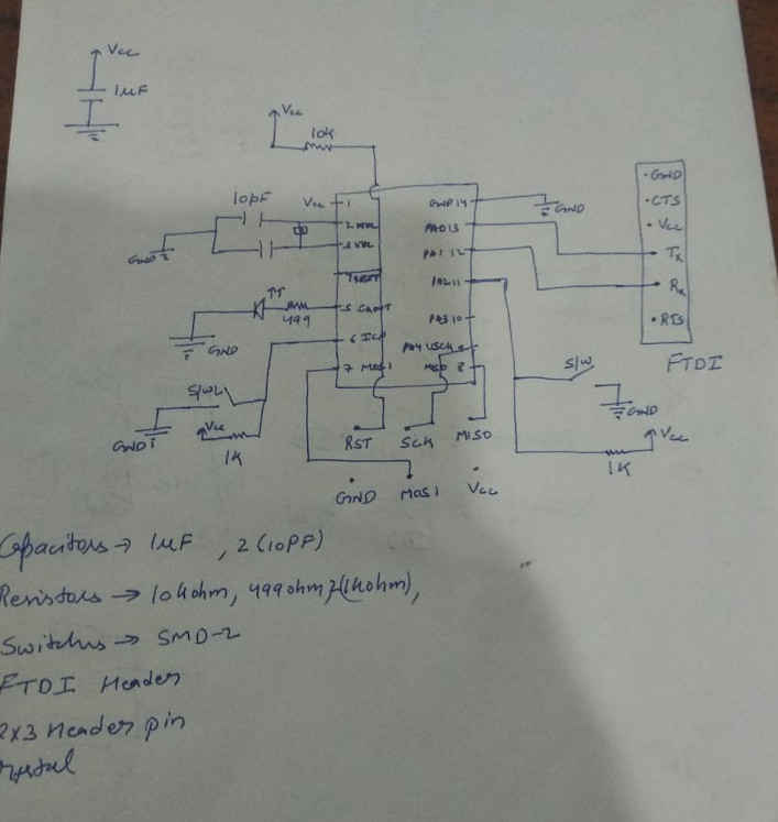
I started with picking the components from the fab files library and putiing them on the schematic page.
| Quantity | Component |
|---|---|
| 1 | Atiny 44 14 pin microcontroller. |
| 1 | Crystal |
| 1 | 1 Kilo Ohm resistor. |
| 1 | 1 micro-farads Capacitor. |
| 1 | 3x2 AVRISP SMD connector. |
| 1 | 6 pin header. |
| 2 | 10 Pico farad capactior |
| 1 | 499 Ohm Resistors. |
| 1 | 6 MM Switch. |
The components selected are of 1206 size. the 12 and 06 means .12X.06 inches so it is important that we take the components of the same dimensions.
The components selected are of SMD and not through hole.
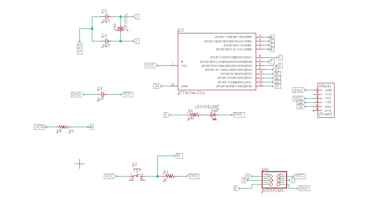
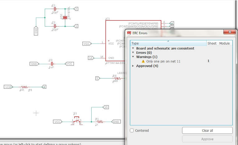
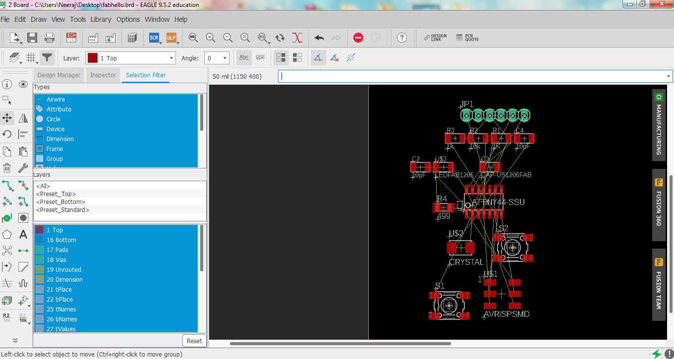
the schematic is prepared and now we have to create the board and before that we have to run ERC at the command board which asks for the apporval of the things which the software asks.
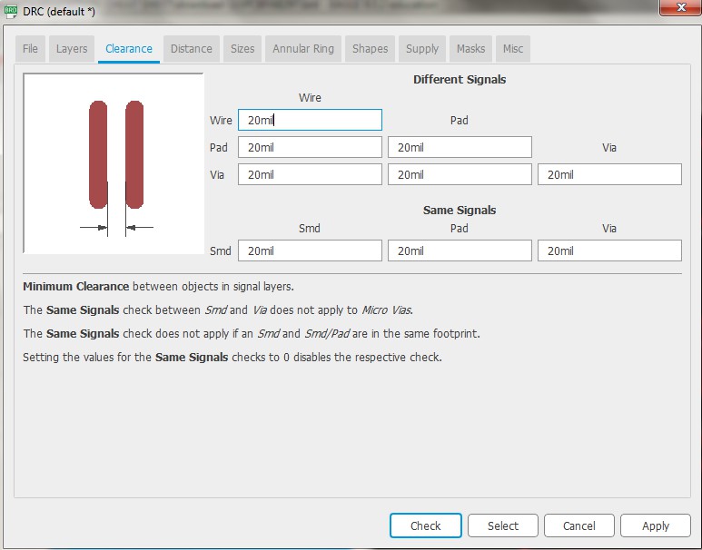
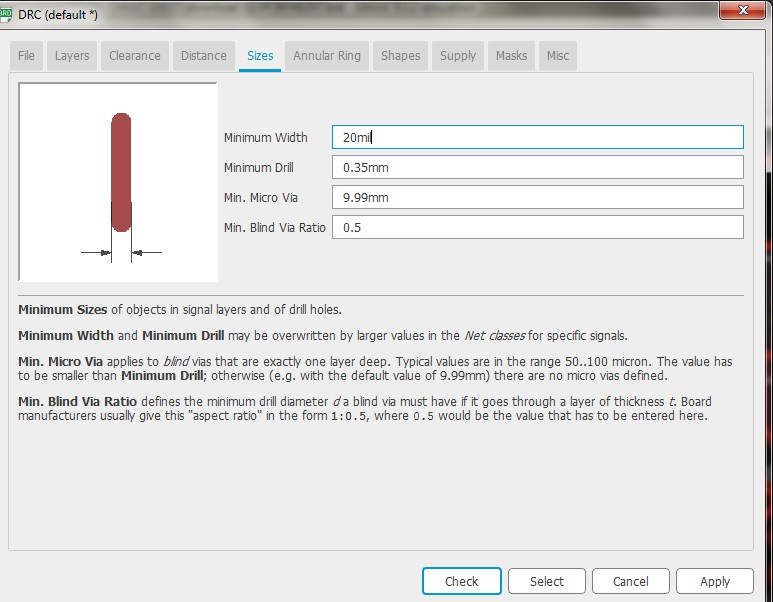
Then you need to apply DRC for the design rules. the design rules of the SRM 20 has to be the input to the DRC. The minimum thickness which can be cut by the machine has to be the input.This step is crucial to ensure that we are applying enough constraint on the design so the milling bit would engrave the traces and pads of the components correctly ensuring that the design would function properly and reliably.
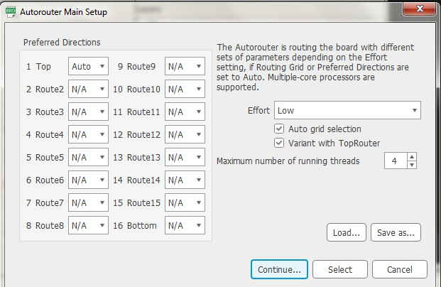
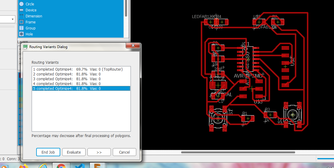
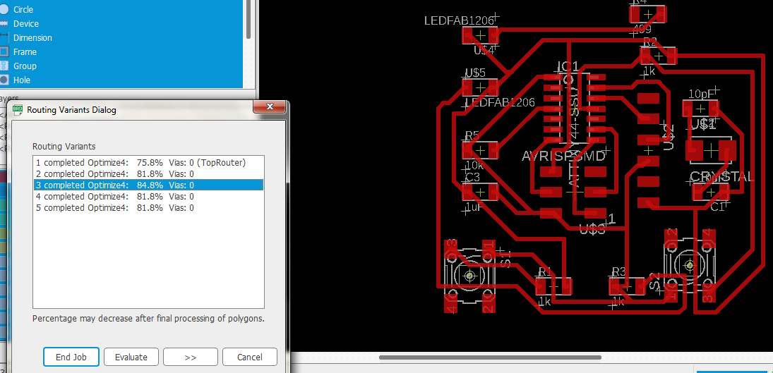
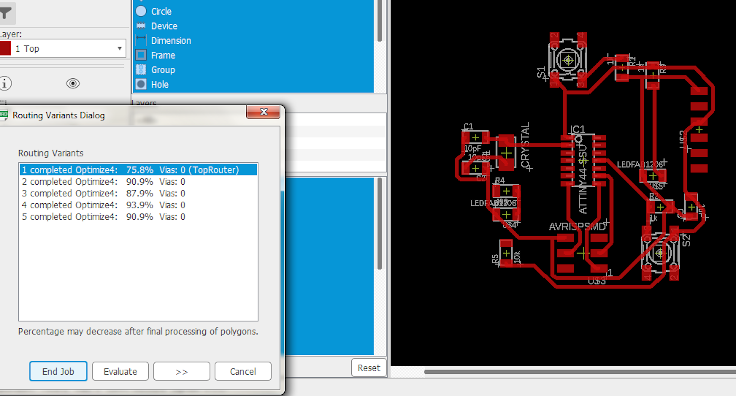
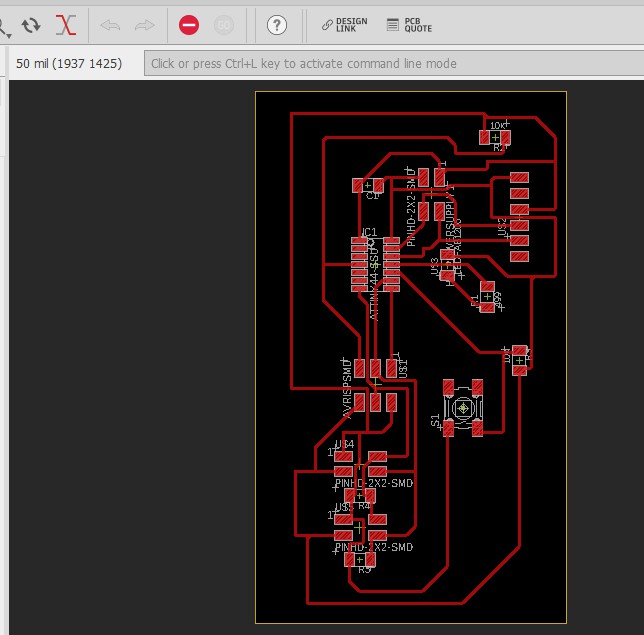
Then comes the difficult part where we need to optimize the board design using he different tools in the eagle toolbar.Ratsnest simplifies the design by moving the path. The Autorouter designs the path with some percentage of optimsation.
Initially i picked the through hole pin which i had to change afterwards. The result after initial ratsnest and autorouter was not properly optimised.
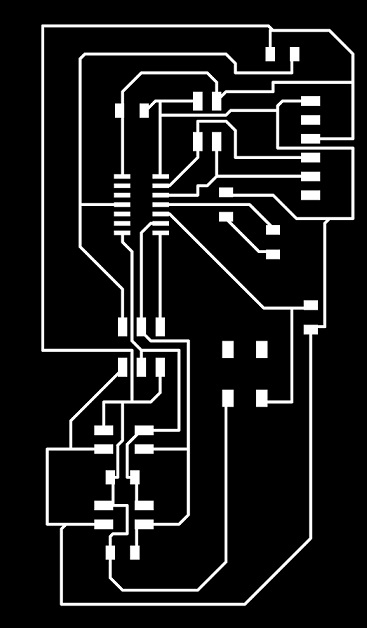
To export my board as an image by going to file >> export >> image, and change the image characteristics. I chose the maximum resolution value 2000 dpi and checking the monochrome box.
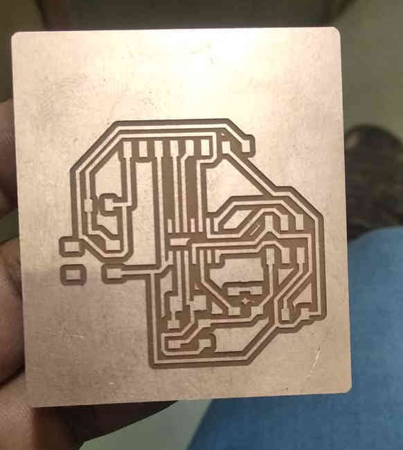
The pictures are then saved in the directory of my choice in PNG format. I used paint editor to edit the traces image and create the outlines by simply Covering the traces with a white filled BOX.
Then I used the fab modules to create the .rml format for my traces and outlines. The exact steps for the process can be found on my electronics production page.
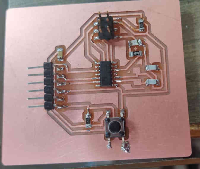
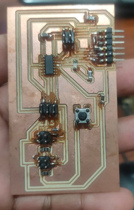
Then soldering of the components was done on it.
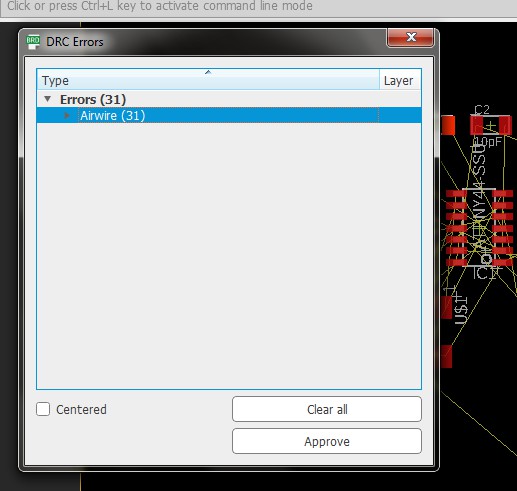
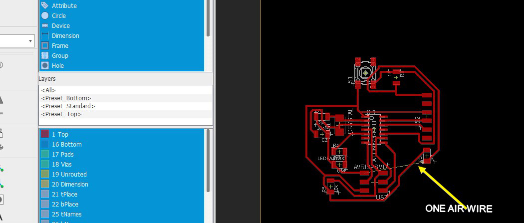
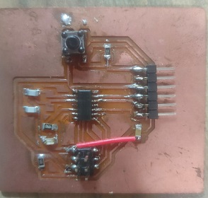
I soldered the PCB with one airwire left. I did not know that if all the airwires are not removed then the PCB is not going to work owing to my mechanical engineering background and i then realized that i had to remove all the airwires. So all the subsequent PCB's which i designed later i made sure that there should not be any airwire left on it. I could have soldered a jumper wire in place of the airwire but then i thought of designing the PCB again with no airwire.
Mr Salman(my global evaluator) has asked me to complete the board and it is not a good practice to abandon a board lke that. So i started searching for the board and i did not find it. The next day i again tried to find it and i found it. I made the modifications to it and was able to upload the program on it.
I found the PCB with many components desoldered and i soldered the missing components again and found that there was an error in uploading. I had to check for the continuity and i found that the board was my first one and i had some cold solder on it. I again soldered all the cold solder and again found that the progra was not getting uploaded. Then i decided to change the microcontroller and after the MC the code got uploaded easily.
Download corrected eagle file
After Lockdown
I made a new board after the lockdown since now i have the knowledge of the assignments so i designed my board such that it can be used for all other assignments. Like i have given multiple rx and tx pins so that it can be used in the networking week. I have also used FTDI so that i can give power and communicate it through various assignments.
The process for designing the board is explained in the above design.
I realised that it is fun designing electronics if you know proper bsics of the software in which i was lagging initially since there are limited resources online which explain detailed explaination of eagle.
In this design i have given two pins of SCK and MOSI to have I2C communication and two pairs of RX and TX to have serial communication for the communication week.
I also desiged a slave board for the networking and communuication week by doing some small modification in the master board itself.
Now since i have soldered a lot of PCBs, i find my soldering quite nice as compare to the earlier soldering i was doing.
Download rml file
Download eagle files
I loaded a program on to it to see its working so i uploaded the blink program to it and it was a delight to see it working
The program for Blink is
                            /*This work by NEERAJ GUPTA is licensed under a Creative Commons Attribution-ShareAlike 4.0 International License.*/
                            const int buttonPin = 3;     // the number of the pushbutton pin
const int ledPin =  2;      // the number of the LED pin

// variables will change:
int buttonState = 0;         // variable for reading the pushbutton status

void setup() {
  // initialize the LED pin as an output:
  pinMode(ledPin, OUTPUT);
  // initialize the pushbutton pin as an input:
  pinMode(buttonPin, INPUT);
}

void loop() {
  // read the state of the pushbutton value:
  buttonState = digitalRead(buttonPin);

  // check if the pushbutton is pressed. If it is, the buttonState is HIGH:
  if (buttonState == HIGH) {
    // turn LED on:
    digitalWrite(ledPin, HIGH);
  } else {
    // turn LED off:
    digitalWrite(ledPin, LOW);
  }
}
Lab Test Equipments ( Group Project )
Multimeter
A Multimeter is basically a Paramter measuring tool, which can measure a wide range of parameters, Principally : Voltage (AC/DC), Resistance, Capacitance, Conductivity etc. Its the most common diagnostic tool technicians have, through multimeter debugging comes handy.
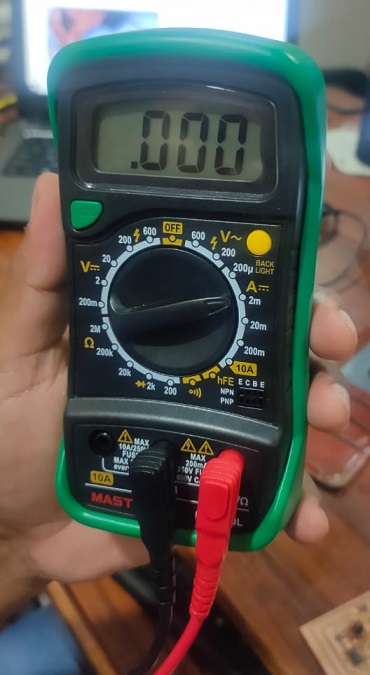
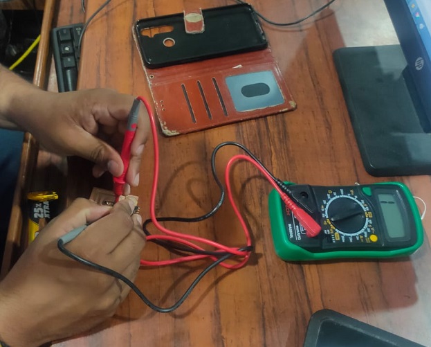
For every debugging and troubleshooitng, Multimeter was there for our rescue. I cant imagine electronics without multimeter.
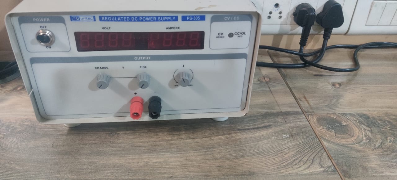
Power Supply
In our lab we have Regulated DC power supply PS-305. It is also very useful as it can supply any voltage you need for the testing purpose.
Oscilloscope
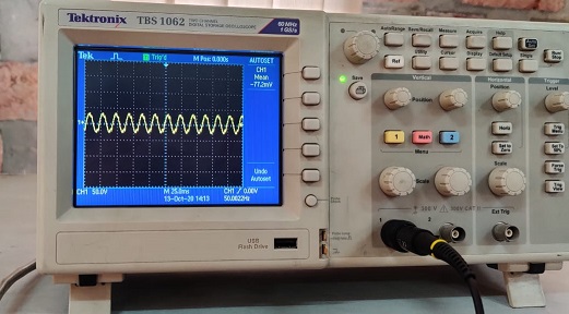
While working with electronics, for debugging and testing behavior, we need to understand the circuits on signal level, which multimeters fails to do. In this case Oscilloscopes come in picture. A digital oscilloscope measures the signal, and then converts that measurement into a digital format using an ADC converter, after which the data measured is depicted as a digital waveform representation. From this representation various paramters can be evaluated.
Key Features
1. 16 automated measurements, and FFT analysis for simplified waveform analysis
2. Built-in waveform limit testing
3. Automated, extended data logging feature
4. Autoset and signal auto-ranging
5. Built-in context-sensitive help
6. Probe check wizard
7. 5.7 in. (144 mm) Active TFT Color Display
8. Multiple-language user interface
9. Small footprint and lightweight - Only 4.9 in. (124 mm) deep and 4.4 lb. (2 kg)
Measuring Digital Signal:
We uploaded Blink code on the UNO board and we observed the pulse signal.Above are the results for the same.