ELECTRONIC PRODUCTION
So This week we are going to mill some PCB. I had studied electronics
in my first year and from then I have not worked on it so i have very less knowledge and experience about it.
I asked my instructor how this week is going to be for me, he said that i just need to know ABCD alphabets and
that will be enough for this week. And so with the confidence given to me by my instructor we started with the
group project but soon to realise that we don't have the end mills and other components required for the group and
for the individual assignment.
We enquired about it and came to know that the reason behind it is 'CORONA' and supplies from China
are stalled. Alas!
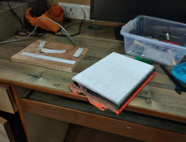
But we had copper tape with us and we have already worked on it before so we started cutting the PCB with vinyl plotter. gfgfgfgf
I read some pages of the previous students and found out that we have to download
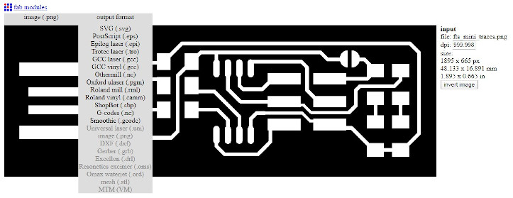
image of PCB in PNG format I downloaded the file and imported it to Graphtec
software for the Vinyll plotter.
The trace is availaible on this
link
The Outline is availaible on this Link
I set the threshold value at the optimum level after many rigorous iterations but the size of the PCB cut by vinyll was big as i had forgot to reduce the dimensions.
I found the size of the PCB after looking in the Fab Academy pages.
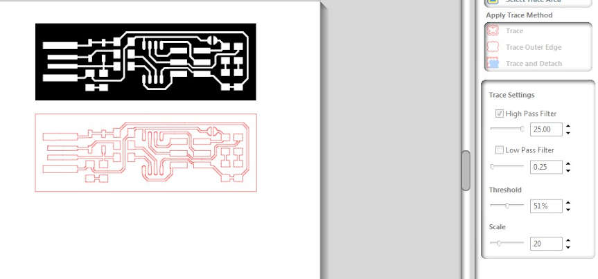
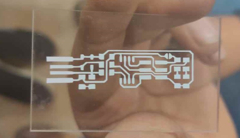
Then I started with the smaller size and tried with different threshold level and the size which I found to be accurate for the small size PCB was (.8*1.72.inches)
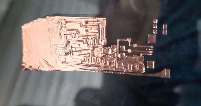
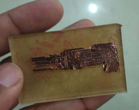
And then we started replicating this with the copper tape.
.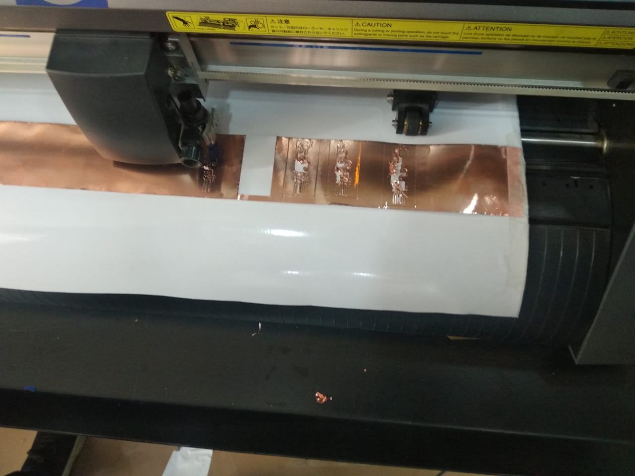
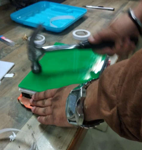
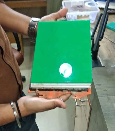
I tried at different speed and power and was frustrated with the number of experiments.I treid with speeds I thought that the quality of the Copper tape was not good. The shapes avaialible on the drawing were not created on the copper sheet. i tried with different settings. The copper tape was put on the vinyll sheet without seprating the adheisve and placed between the holder which didnot work. I also tried to stick the copper tape directly on to the vinyll sheet which also didnot work. The cutted part was coming out and when the blade was crossing the same path, it was taking away the required path of the PCB.
My instrutor Mr. Rahul also tried with different settign and with different materials. We tested by apllying the copper tape on the vinyl sheet we also tried on the sacrificial layer of the vinyl sheet. we found that there is something wrong withthe settings of FORCE and SPEED.
| Force | Speed |
|---|---|
| 10 | 10 |
| 12 | 10 |
| 14 | 10 |
| 10 | 12 |
| 12 | 12 |
| 14 | 12 |
| 10 | 14 |
| 12 | 14 |
| 14 | 14 |
I asked my instrutor and and we did a lot of experiments but we found out that there is something wrong with the plotter since the trace mapped in the software was not seen at all places of the cut and now it will get repaired in few days.
Group Assignment
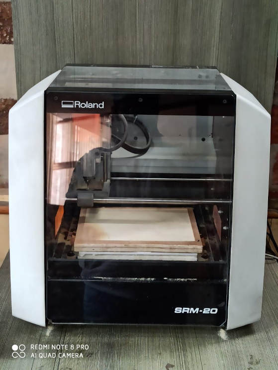
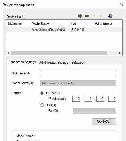
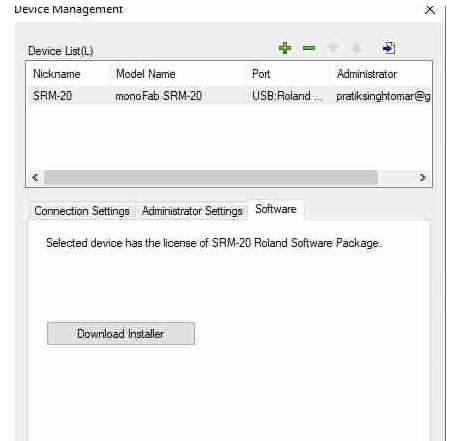
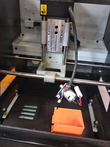
Hurray We have got the supplies of the bits and now we are upto start with the milling process. My laboratory has a monoFab SRM-20 compact desktop milling machine (basically a miniature CNC mill, from Roland DGA Corporation (Irvine, California, United States), and that is what I used to produce PCBs for myself. The mill is computer-controlled through a program called VPanel for SRM-20, also from from Roland DGA Corporation. It is used to output toolpaths (cutting data) to the mill. The toolpaths were created at fabmodules.org.
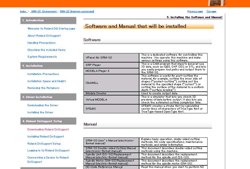
You can download the software which is used to operate on Roland machine from this link.
Installation process
The preocess for installing is below
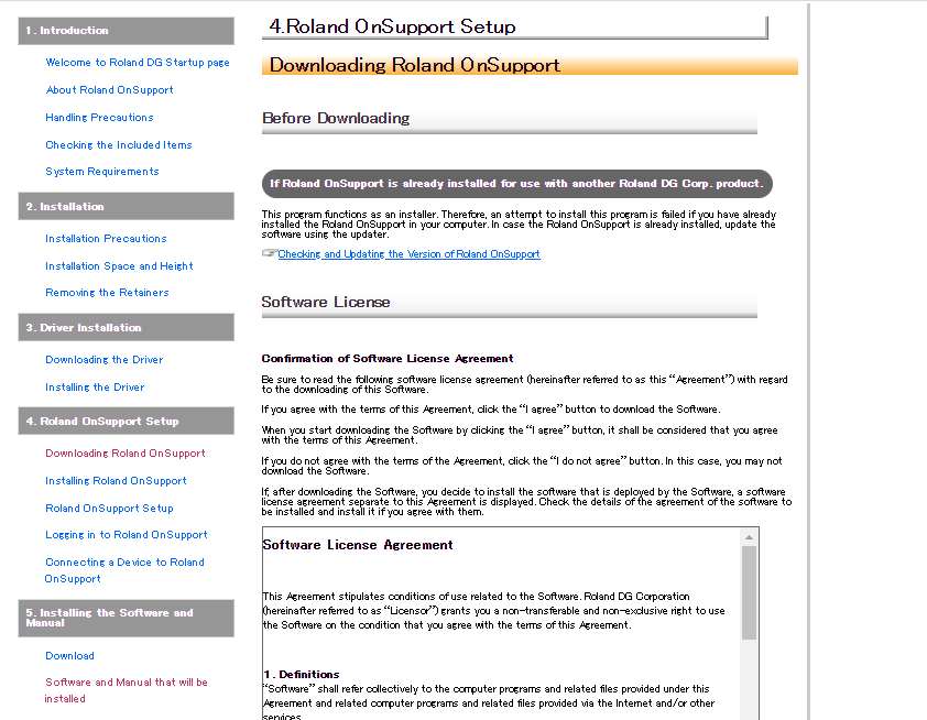
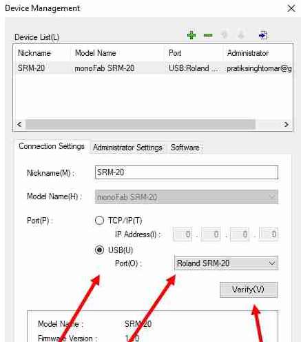
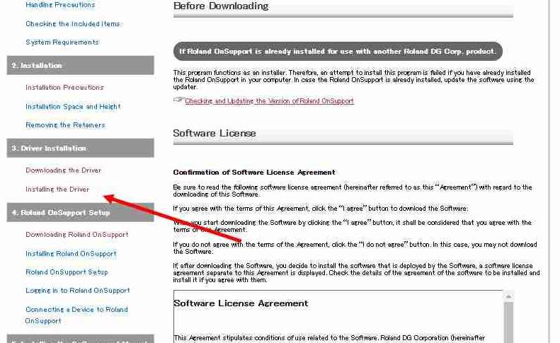
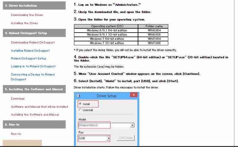
The installation process is a bit tedious as compared to the installation of other softwares. So you need to be patient while doing this.
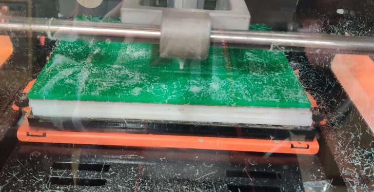
We start surfacing the bed so that it gets leveled up. The bed is made up of three layers of acrylic and three layers of wood .
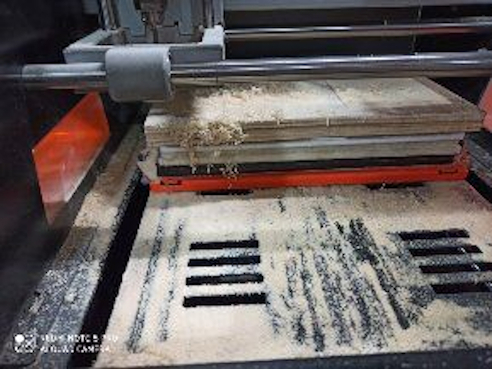
The result obtained was weird , the hair like structure was easily visible and the mill was
not uniform because of the bed level.
We checked the bed again and found that it is leveled.
The bed was aligned and we started to mil the piece.
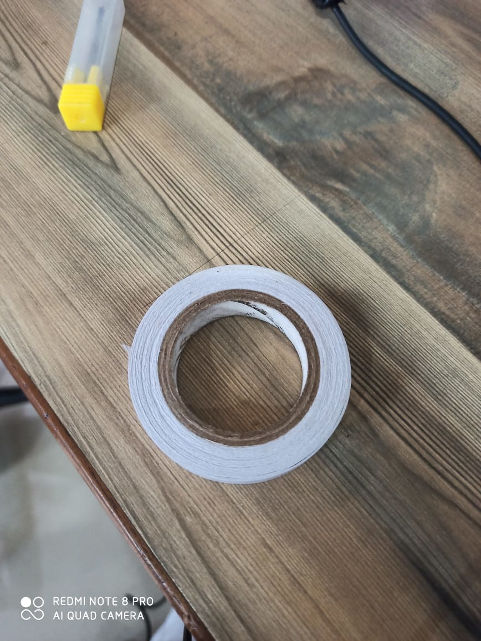
The milled PCB was not upto the mark as we had done a mistake on the bed. The double sided tape which i put underneath the bed was uneven and because of ehich we got diffrerent depths.
I also used the thicker double sided tape which was also the reason for not getting the even milling
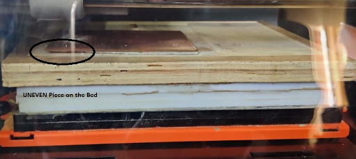
Before proceeding with the second trial i again checked for the bed level but i found that the bed is now not leveled. I tried applying force in downward direction but the level was not attained again.
My instructor Mr. Rahul decided to change the wood layer and replace it with the Acrlic layer.
So i calculated
the length and width of the bed and cut it with Laser cutter.
The assembly part of the machine was also disassembled since there was noise while running of the motor. We assembled that again but the noise was coming after that also.
An acrylic sheet was then chiosen to be the sacrificial layer as it is very straight and it does not degrade overtime. The new acrylic plate was glued to the previous acrylic base after removing the wooden sacrificial layer. The dimensions which were used for milling are 150mm and 210mm.
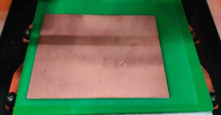
Now we could see the surface milled was very clean and it was even as well.
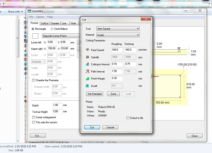
The surface was made unifrom with the help of the software click mill. You need to give it the surface area which you want to level up and the depth and the tool whcih you are going to use and the material which you are going to level.
These are the settings which were used in the clickmill software to level the surface.
The tool used for surfacing the acrylic bed was 2mm end mill which we brought from one of our labs.
The bed size for surfacing was selected as 150mmx210mm and the settings were automatically generated on the clickmill software and the surfacing was done.
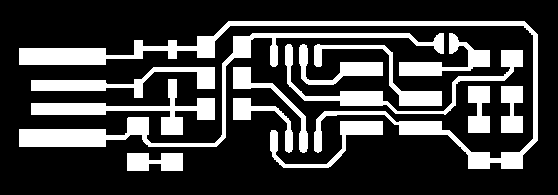
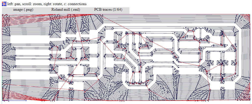
I imported the png image of the PCB to be milled form the tutorial
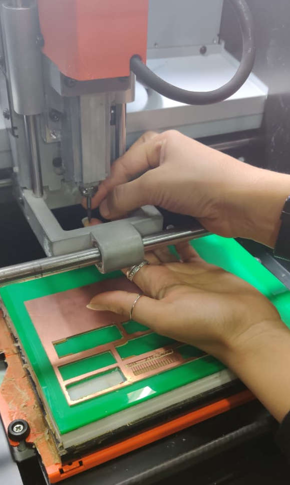
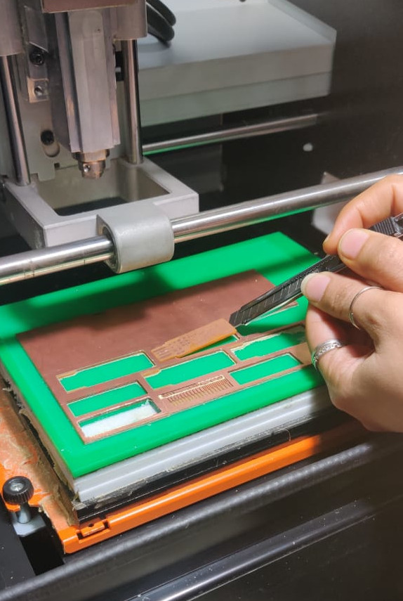
After again surfacing of the bed which took around 6 hours. We started to mill the PCB as we have got our supplies of the bits
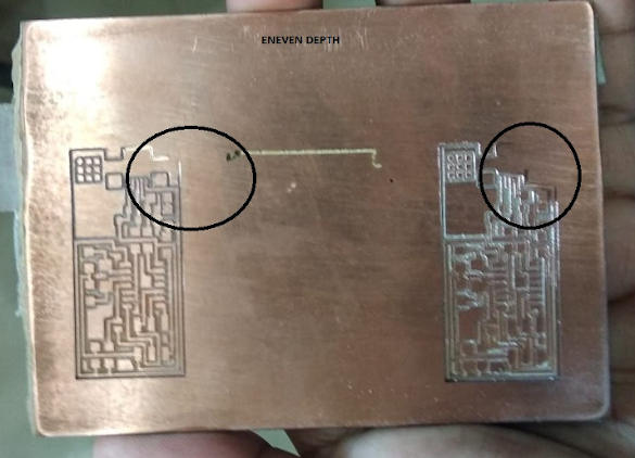
I milled the pcb with differnt offset and different bits. I used a V bit and 1/64 bit for the traces and 1/32 for the outline.
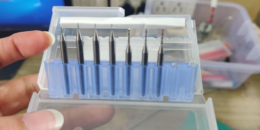
Get all the endmills, double sided tape, PCB board and vaccum cleaner availaible to you
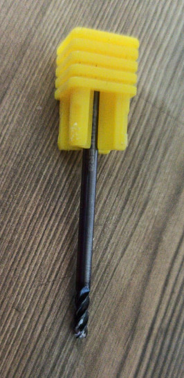
The tip of the end mill is very thin and it can easily break if you dont handle it proeprly. It is important that you put one hand beneath the tip of the tool so that it gets support and does not fall.
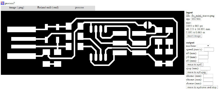
Here is the step by step guide to generate the .rml file
Step1:Open the file (.png) and select the output as .rml
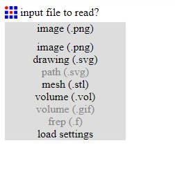
Step 2: Open the file (.png) and select the output as .rml
Step3: Now select the process as PCB Traces (1/64) as we are going to mill the traces for outline we'll use PCB Outline (1/32).
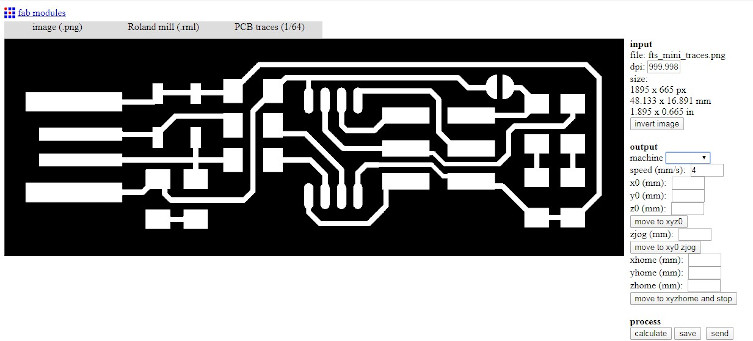
Step 4:Now set the parameters as : and then click on save to download the filel
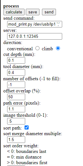
>The tool path is now visible. In my case the tool offset is taken as -1 which will ensure that the all the copper is removed expect the required one.
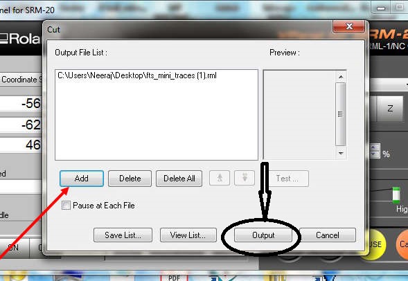
Step 5:Now after downloading the RML file, it is time to mill out the board on the V panel for SRM 20
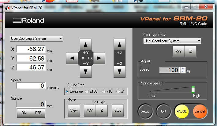
Step 6: Now go to CUT button and select the downloaded RML File followed by clicking on Output
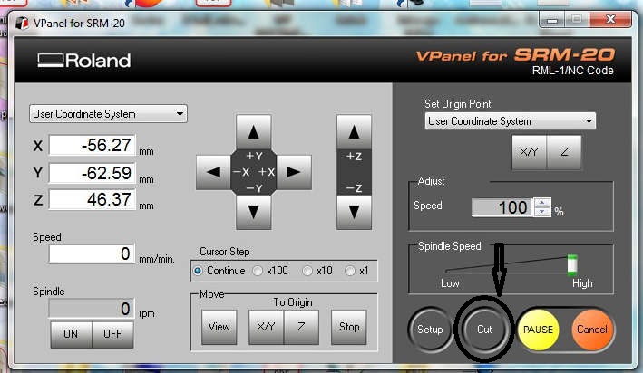
The V Panel is used to operate the SRM 20 machine. It is used as the interface between the machine and the CAM file whcih you have created for milling. The panel is userfrindly and you can directly control the movement in the all the three axis. But at the same time it should be operated very cautioulsy since the tools which we are going to use have very small diameter and very less impact strength so if the spindle touches the bed with even a smaller force then it can break so when the tool is present in the collet then the software has to be taken care of.
The interface of SRM 20 is easy to use but it is important to be very careful to plug in the endmills as they can break very easily. There are options on the interface to use machine coordinate system or user coordinate system. The machine coordinate system will always put the spindle on one side of the bed irrespective of the defined coordinates. I had mistakely ticked the option of machine coordinate system and the design of the PCB came out was not proper as it is very difficult to arrange the spindle on to the same coordinates as they were before to cut the outer shell of gthe PCB.
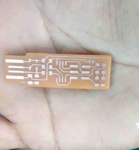
The PCB were milled at different offsets. I used -1 and 4 at 50% offset percentage. The -1 offset doesnot leave any copper behind on the clad board other than the intended one. Note: The design was taken from this webpage
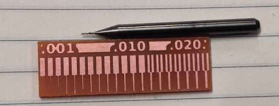
1/64" BIT
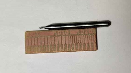
V BIT
We used three types of tool to mill the test piece. The tools used were 1/32", 1/64" and v bit. The 1/32" tool is used to cut the outlines whereas the other two end mills are used to cut the traces on the PCB. The traces are clean while using 1/64" mill but while using the v bit you can see the hair line copper remaining in between the traces a which can be a pain while soldering or prograamming so we need to do postprocessing on ther PCB while using V bit for traces.
It can be seen from the test cut that the mill till .013 inch is done by the machine. The path under this dimension can be milled on the machine. The lines till .006 inch was not printed by the machine so this is the limitation of SRM20 with 1/64" tool. The v bit also showed that the clearence can be abtained till .013 inch and it can mill the line till .001inch. The process of milling is explained in the later part of the page.
>Completing the PCB milling was satisfying as we started after many days due to problem in the supply chain.
Now it is time to do some soldering which is of Surface mount Components. I did soldering many years
before and now again i am going to do it. Excited!
this is the list of the components which we are going to solder in the PCB.
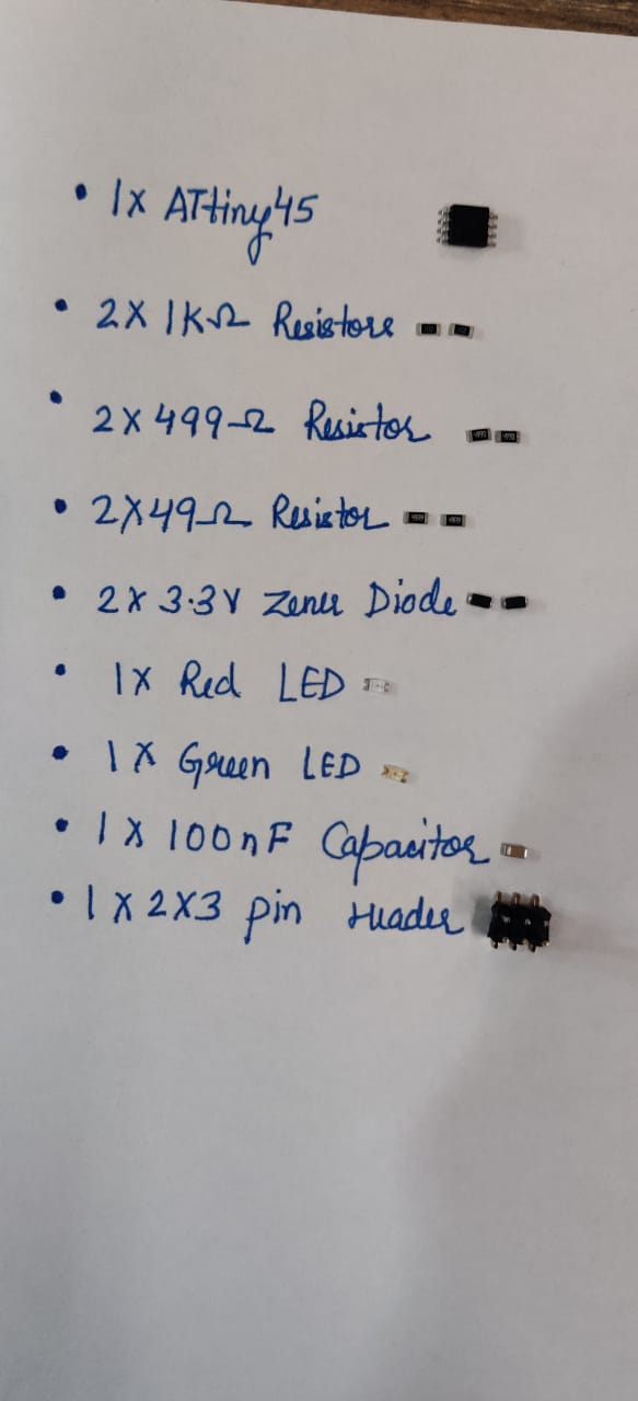
>These are the surface mount which we are going to use during soldering SMD components
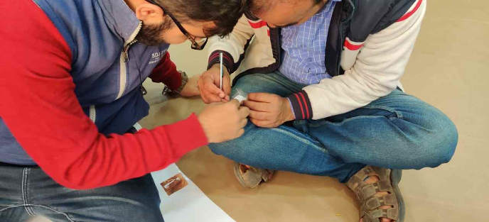
You need to be very patient while soldering as the components sizes are in mm and they will fall out of your hands if you are not careful. And if they fall on the ground then it becomes a maze to find it. I used twizzer which helped me to handle the components better. i saw this video. it is important to get some idea about soldering before you actually start to solder. my instrutor also taught me to solder. The polarity of diodes should be kept in mind before soldering becuase it can cause a lot of pain while desoldering those tiny components.
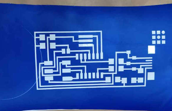
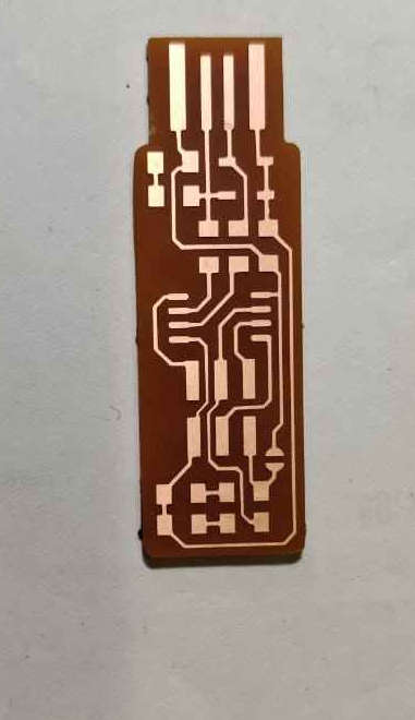
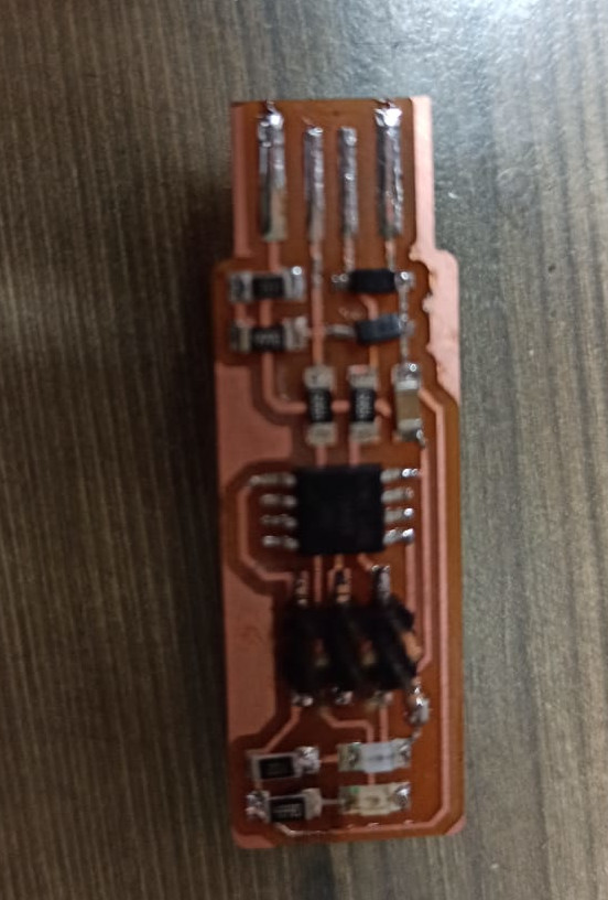
Hero shot of my PCB
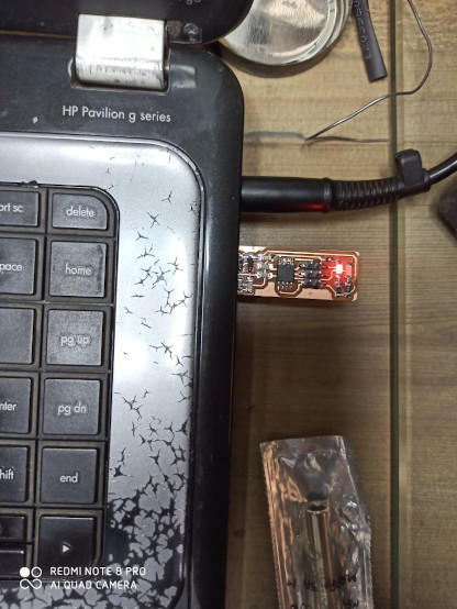
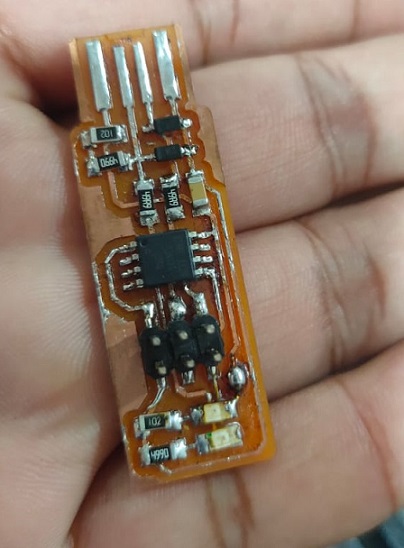
I am stunned to see my PCB working on my first attempt. The light is on and i am on seventhn cloud. But there is programmning to go and i am a zero in it.
Now i have program the the PCB so that it is able to progam other PCBs.
I started reading the fabacademy pages and i found that i need to install some softwares to do it.
This page
gives a detailed description about how to program the PCB and what softwares to download.
The programs that I have installed are the following:
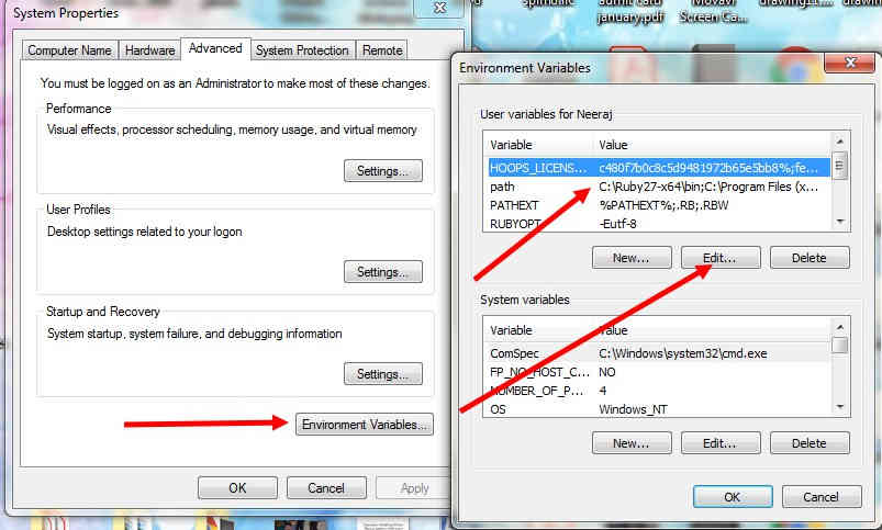
Then I added the paths of GNU toolchain, GNU make and AVRDUDE by going to the control panel >>
system and security >> system >> advanced system
settings >> environment variable >> double click on paths >> and add the
new paths.
Then i installed Zadig
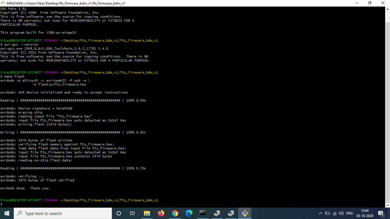
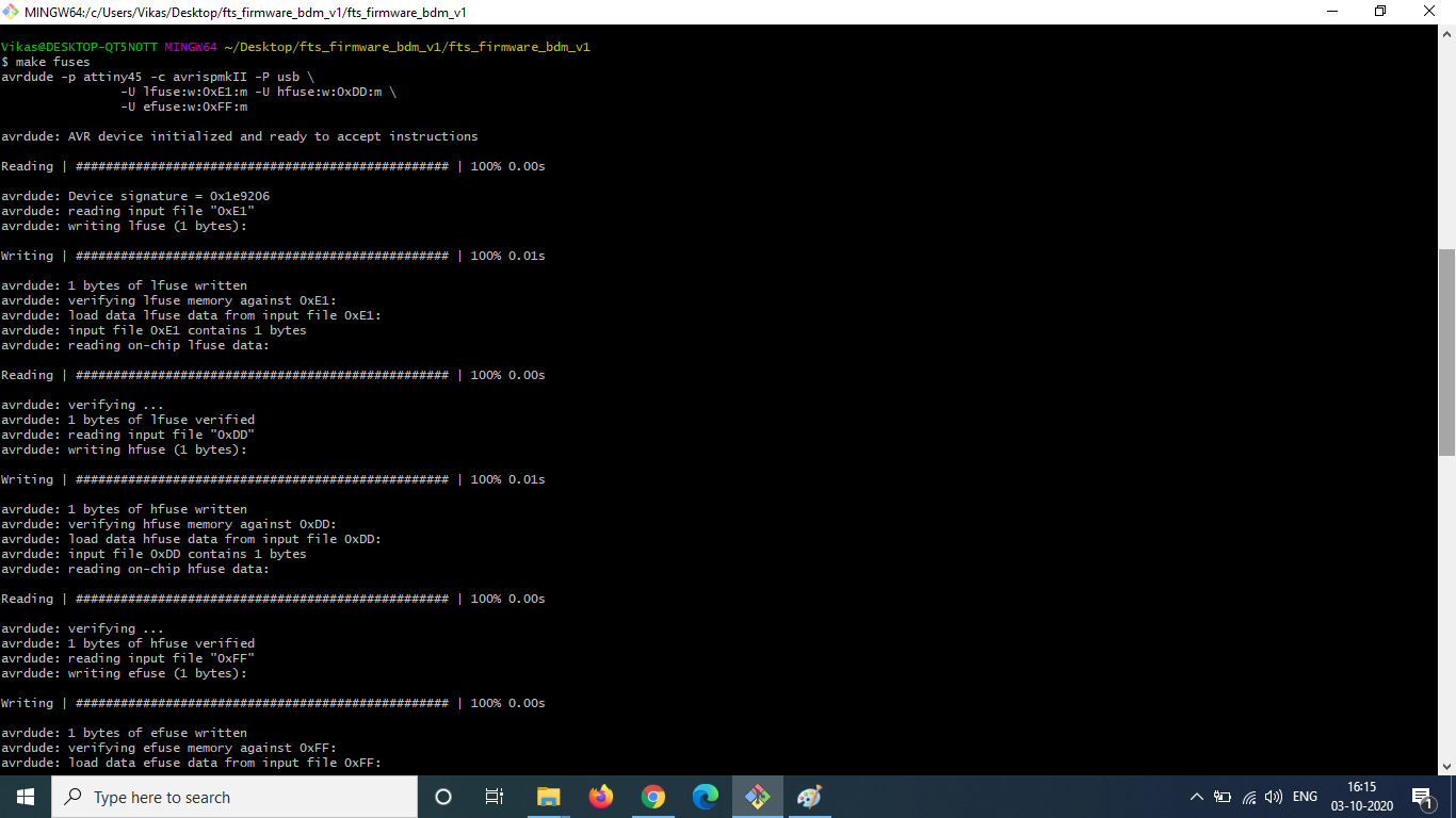
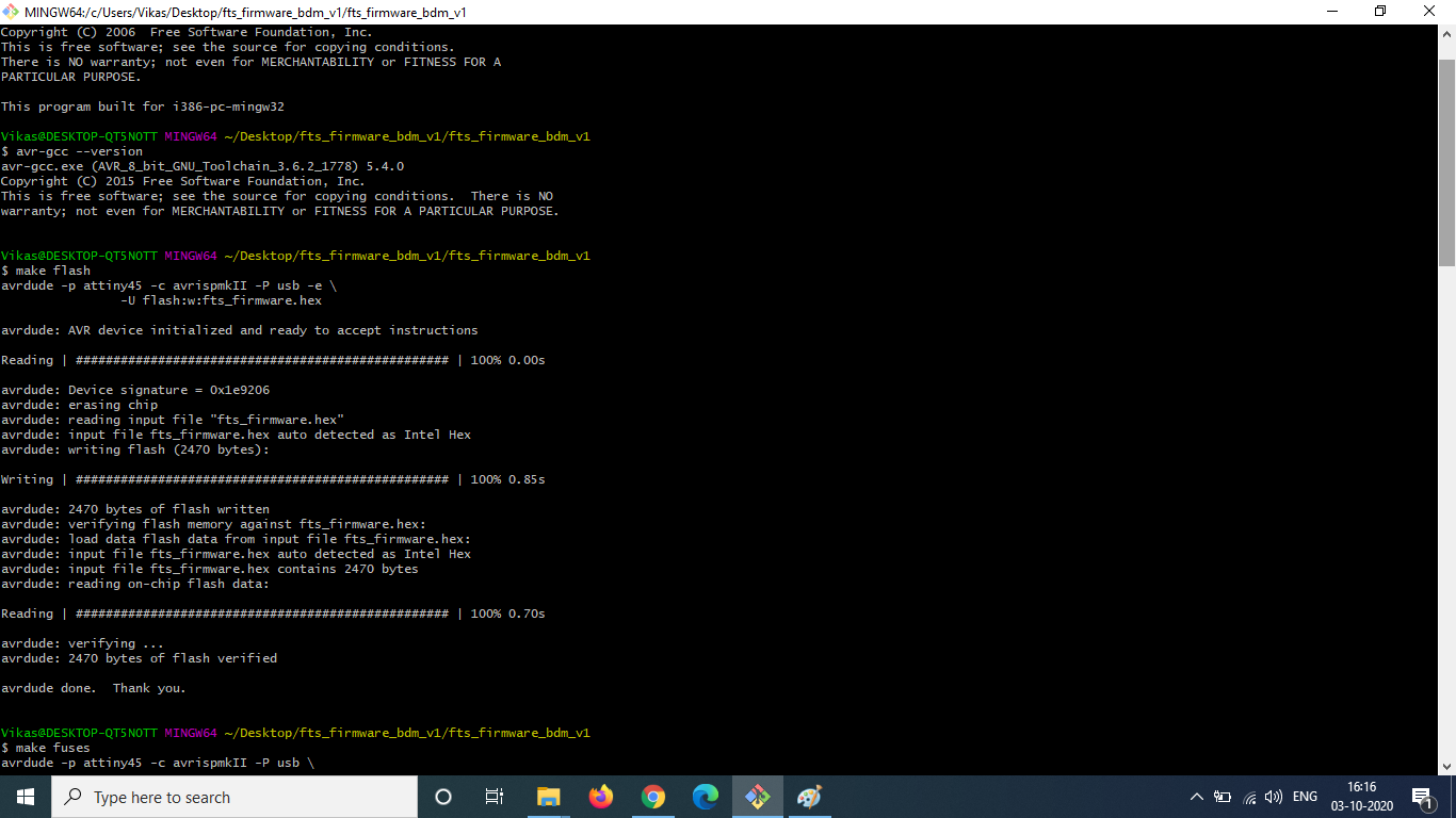
Next, I opened the firmware directory and ran make to create a hex file. Once the hex file was created, I carefully plugged in my USB connector and the ISP board which is avrispmkii. Then I ran the commands make flash in gitbash. The command erases the target chip (my board) and programs its flash memory with the contents of the .hex file created previously.
I am having windows 7 and there is some problem relating to the path and the USB ports are also not working so i am using AFSHA's laptop for it.
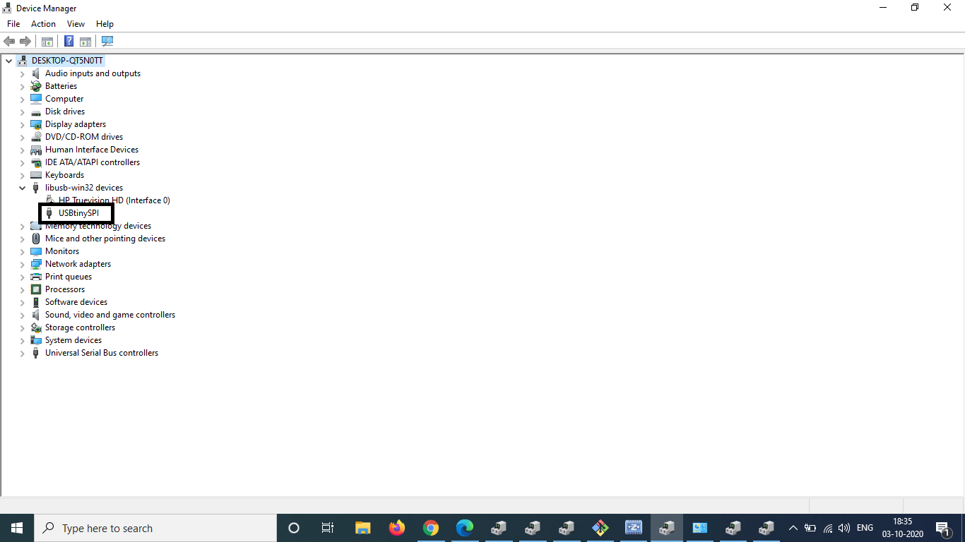
To check the USB functionality, I had to plug in my own board directly and check if my computer detects the device.
That is done by accessing the device manager and checking under Universal Serial Bus controllers.
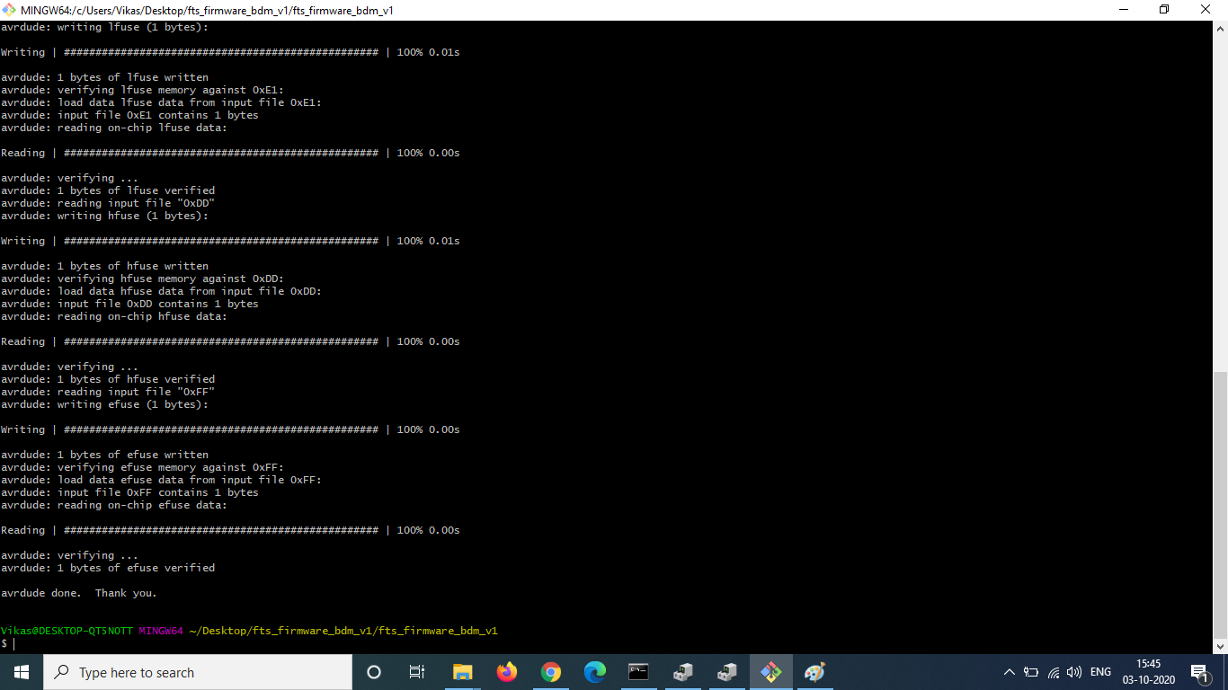
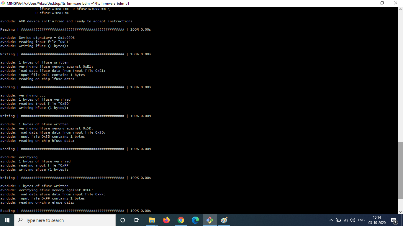
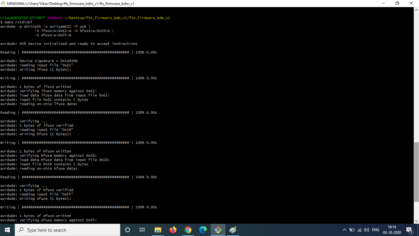
The last step of programming the ISP is to blow the reset fuse by running make rstdisbl. This command will disable
the ability to re-program the board in the future by changing the reset pin of the board to a general purpose input output pin.
Conclusion
The characterisation of the machine was the group task and we concluded that the 1/64 end mill is more effective than the V bit. The Offset which we used was -1 if we want no copper on the PCB and the offset was 4 and the offset percentage was 50%. The cut depth was 0.08mm for the traces and for the outline it was 1.4mm. The tool Diameter is 3.5mm.
Note