
Week 11. Input Devices
11. Input devices
Assignment
Group assignment: “Measure the analog levels and digital signals in an input device”
Individual assignment: “Measure something: add a sensor to a microcontroller board that you have designed and read it.”
Software
Logic Analyzer software
KiCad (Design software for schematics and PCB-design)
Arduino (IDE to write code for the ATTiny)
AVR-Dude (software that allows us to talk to the ATTiny board via the USBTiny)
Hardware
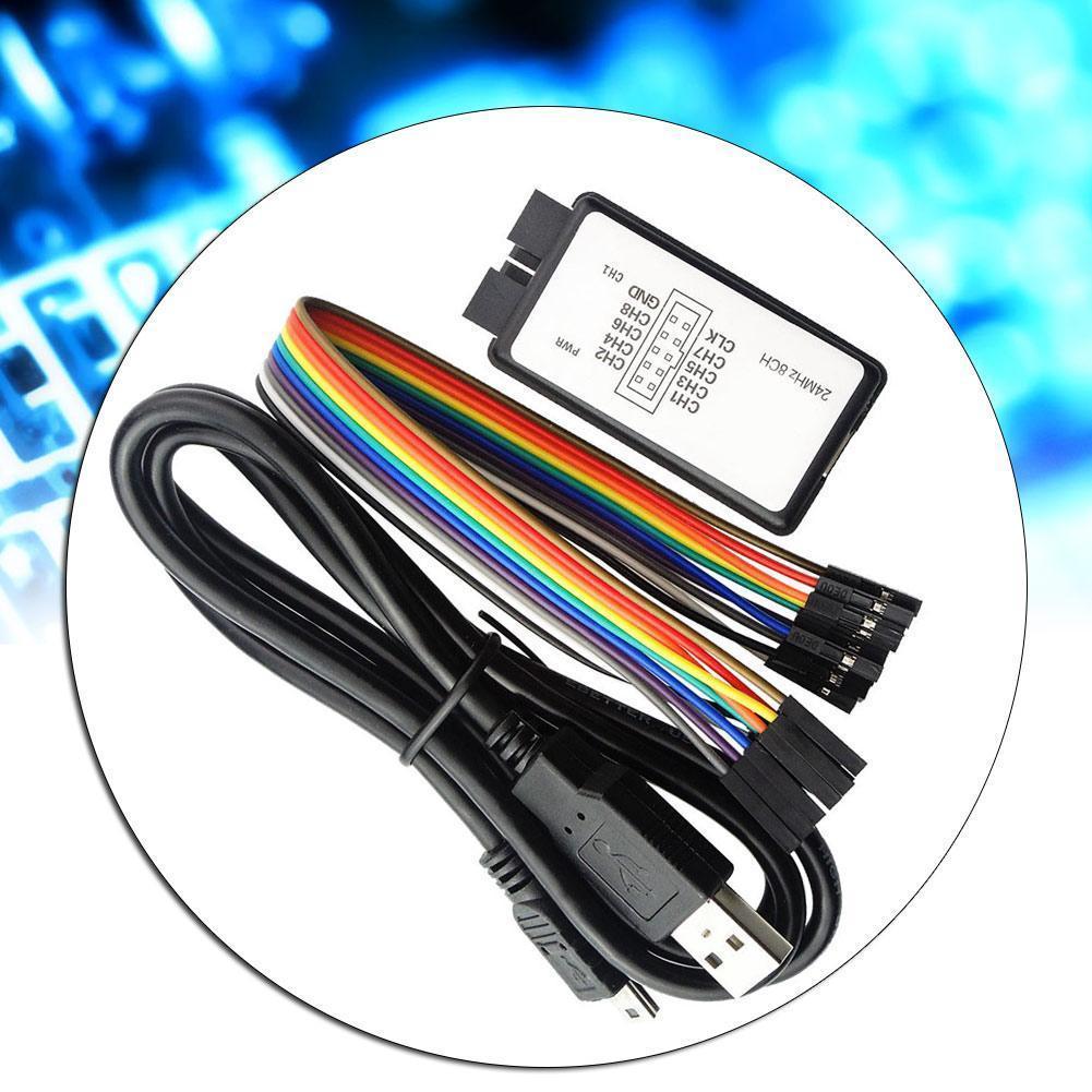
Logic Analizer - 5V 24MHz
USBTiny
Roland Modella MDX-20 mill
with the mill bit for traces - mini end mills two flutes 0.40 mm 826 (damen.cc)
with the mill bit for cutout - two flutes 0.8 mm
Multimeter
Knife
Anti static tweezers for electrical components
Solder iron
Solder tin
Heatgun
Various surface mounted components (ATTiny 44, ect)
Components for acceleromter: ADXL343, 1µF capacitor, 2 10kOhm resistors and a 3.3V converter
acceleromter+gyroscope board MPU6050.
Files
Arduino and MPU6050 sketch
ATTiny and MPU6050 sketch
ATTiny and MPU6050 modified for ADXL343 sketch
ATTiny and ADXL343 sketch
Arduino analog to serial sketch
KiCad schematic and PCB Design
Improved KiCad schematic and PCB Design after noticing errors
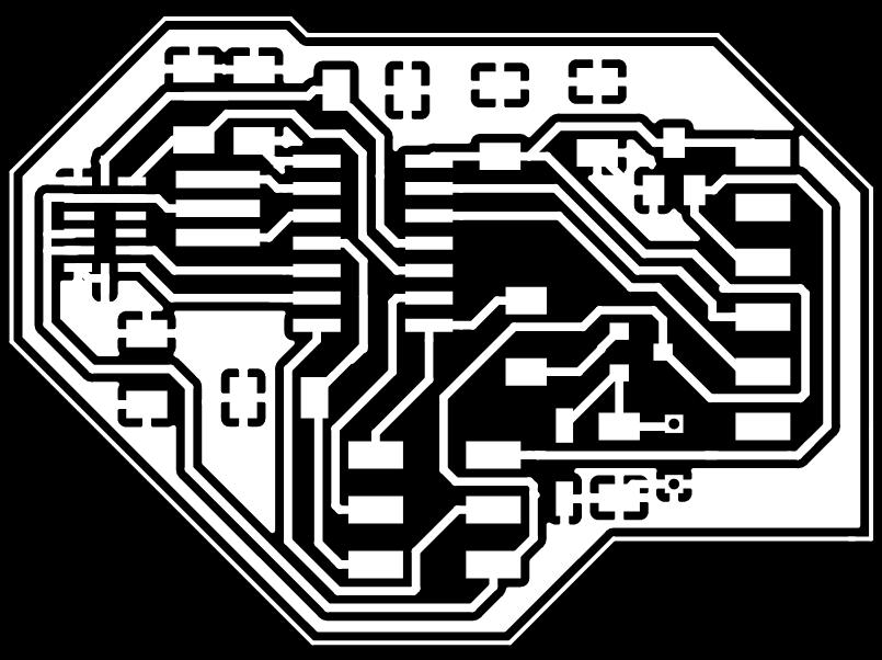
Traces image for mill
Holes image for mill
Cutout image for mill
TIKTOK micocontroller code (Arduino) with accelerometer, vibration and BLE
Group Assignment
For the group assignment we measured a signal of one of the pins of our ATTiny board using the logic analizer.
Our analizer supports up to a 5V connectioan and a maximum sample rate of 24MHz and you can connect up to 8 channels.
The nice thing about a logic analizer can not only visualize a signal, but also show the data. For example it can analyze the data send over an I2C and serial line.
First we uploaded a sketch to our hello world board to send our senso data (for example light seensor) over the TX line.
You use the analyzer by first installing the visualization software on your computer.
Next you connect the GND to the GND of your board.
After the GND you connect one of the input pins to one of the pins of your board. We used our TX pin or our hello world board.
You connect the analyzer to your computer, launch the software and select the analyzer, used pins in the software, and the amount of tiome we want to record.
Video of saleae.com showing how to use the logic analyzer software:
Now we look at the software on our computer and there we see this:
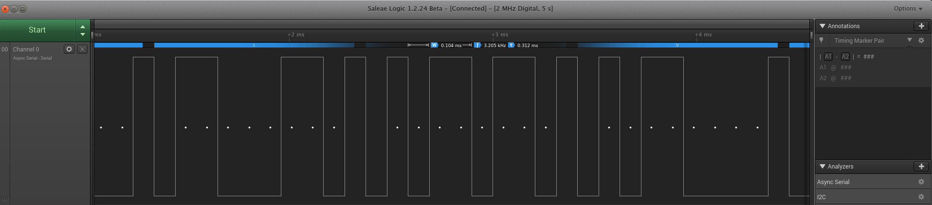
We see that a serial communication goes via high/low (digital) communication.(bottom square wave)
The difference in high/low represents the bits.
Our analyzer then converts the bits to ascii characters using the ascii look up table (blue lines above).
The powerfull thing about this device is that we not only see the quality of the signal, but also the data in a human readable form, that we can analyze realtime, or at our own pace.
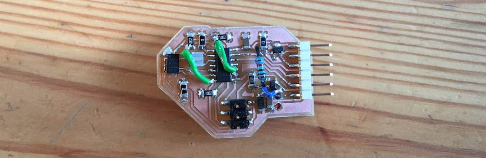
Using a sensor with the ATTiny44
For this assignment we will be creating a microcontroller board with a sensor, and sending the data to the computer. We will walk through the following steps:
- Decide on sensor
- Read about funtionality and usage of the sensor
- Design schematic
- Design board
- Mill the board
- Solder the board using a soldering iron and heatgun
- Write code for sensor and board
Sensor
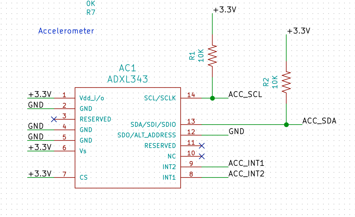
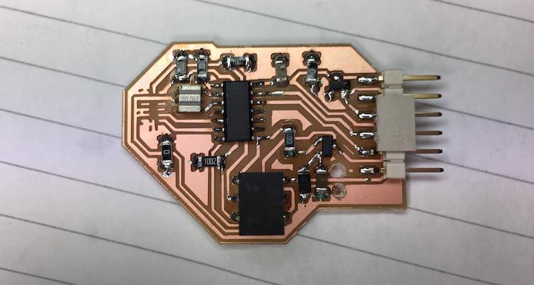
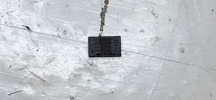
We will be using an accelermeter, the ADXL343.
The ADXL343 can measure acceleration over 3-axis: X,Y and Z, up to 16g.
The device has a maximum operating voltage of 3,9V. (page 5 of the datasheet)
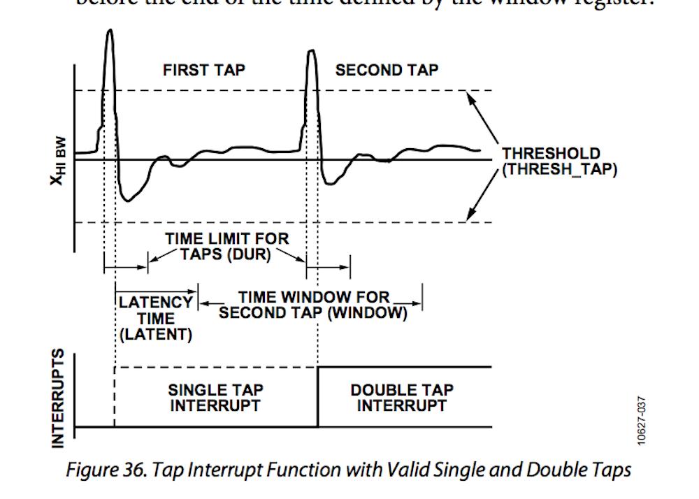
One very interesting thing about this specific accelerometer is that is has 2 build in tap detection features. On page 26 we read the ADXL343 has a build in tap detection feature:
"The tap detection threshold is defined by the THRESH_TAP
register (Address 0x1D).
• The maximum tap duration time is defined by the DUR
register (Address 0x21).
• The tap latency time is defined by the latent register
(Address 0x22) and is the waiting period from the end
of the first tap until the start of the time window, when a
second tap can be detected, which is determined by the
value in the window register (Address 0x23).
• The interval after the latency time (set by the latent register) is
defined by the window register. Although a second tap must
begin after the latency time has expired, it need not finish
before the end of the time defined by the window register"
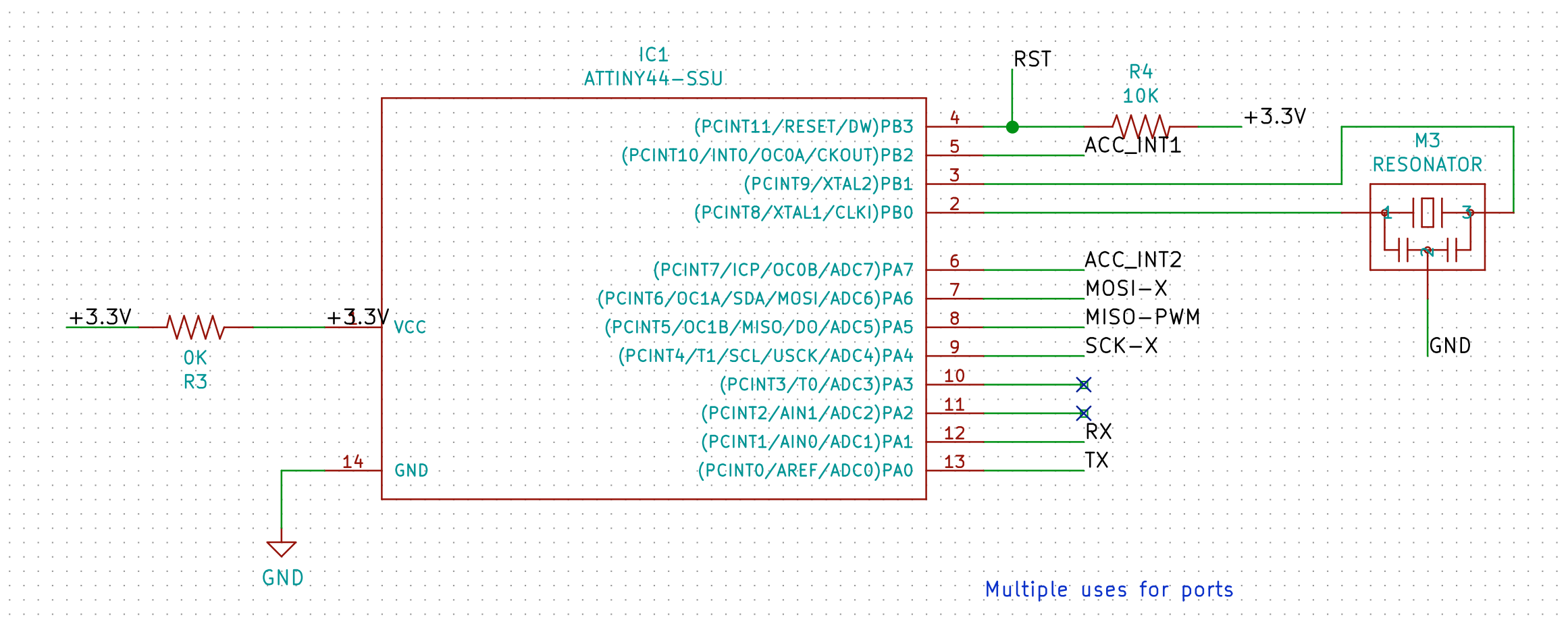
Each tap detection has its own iterrupt pin, we will be needing to connect these pins later to our ATTiny.
On page 13 of the datasheet we find the ADXL343 both supports I2C as SPI. We want to use this device with our ATTiny, and to communicate with our ATTiny we allready use the SPI port, so we will be connecting the ADXL343 to our ATTiny using the I2C ports.
On the Wikipedia page we read I2C is a protocol design by good old Dutch Philips Semiconductors (this division is now NXP).
The protocol is a much used and efficient protocol for communication, it needs 2 wires (Next to GND and VCC): SDA and SCL.
SDA is the dataline
SCL is de clock line
Fun fact: a few years ago I2C had a brother I3C, designed to be even more efficient and it is allready implemented in Linux.
Schematic
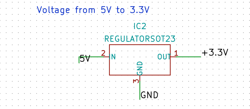
The device has a maximum operating voltage of 3,9V. (page 5 of the datasheet)
In week 7 we made a board that used 5V as directly provided from our computer, now we first need to convert this to 3.3V to not destroy our accelerometer.
We will be directly converting the 5V to 3.3V, allowing our whole board to operate at 3.3V and preventing us to confuse supply lines and to destroy our accelemeter by accident.
On page 6 and 13 of the datasheet we find how the pins need to be connected. Pins 2,4 and 5 need to be connected to the GND. Optionally pin 11 needs to be connected to GND, but this is not explained when this is needed. Further pin 1 and 6 need to be connected to VCC.
For enabling I2C, pin 7 (CS) needs to be connected to VCC, and pin 12 (ALT ADDRESS) either to GND or VCC. We will be connecting pin 12 to GND.
Pin 14 is the I2C SCL line and pin 13 the SDA, we will be connecting these to our ATTiny SDA and SCL pins.
Pin 3, 10 and 11 do not need to be connected.
And last we have pin 9 and 8, they are our tap detection trigger pins.
On page 26 of the datasheet we find we need: “A 1 µF tantalum capacitor (CS) at VS and a 0.1 µF ceramic capacitor
(CI/O) at VDD I/O placed close to the ADXL343 supply pins is recommended to adequately decouple the accelerometer from noise on the power supply”
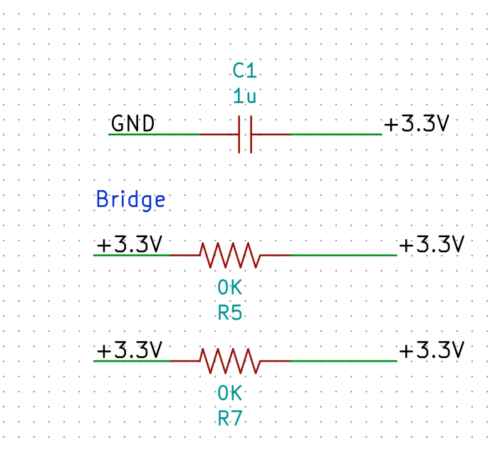
We will supply the same power to both pins, so we will only use a 0.1µF capacitor at the VCC line, we have a pretty simple board and a constant power supply from our USB port, so those will be limited in this case.
For connecting the SDA en SCL pins to the accelerometer I had to be creative, since these pins were also used by my SPI. To keep an overview of my schematic I made a wire splitter design. This will also allow me in the future to make fast changes to my schematic.
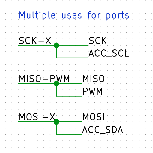
I also designed the parts for week12 in this design with a vibration motor, this resulted in using almost all the ATTiny ports and much difficulties in finding room for connecting everything.
Board design
Placement
In the datasheet on page 26 we find that the ADXL343 should be placed near a mounting point to prevent noise:
“Locating the accelerometer near a hard mounting point ensures that any PCB vibration at the accelerometer is above the accelerometer’s mechanical sensor resonant frequency and, therefore, effectively invisible to the accelerometer. Multiple mounting points close to the sensor and/or a thicker PCB also help to reduce the effect of system resonance on the performance of the sensor.”
We will place our sensor at the side of the board to make sure it is near a mounting board. But overall our board is very small and we will not be mounting this board anyway, so it is a bit theoretically.
The footprint itself is very small as we can see in the datasheet on page 35 of the datasheet.
The footprint design was not available in the fabacademy library. Therefor I thought about design a footprint myself.
But first I looked on the internet if there were footprint libraries available for KiCad. I found that a fellow fabacademy student Ilias Bartolini had designed a footprint for the ADXL343 for KiCad.
I implemented his footprint in KiCad and measured in the PCB editor to see if the footprint had the correct measurements. The footprint was correct, so I did not had to design one myself.
Having everything I need I could start tracing my wires.
I started with the basic schematics using the board design I made in week 7.
I removed the parts I did not needed and added my new components and accelerometer scheme.
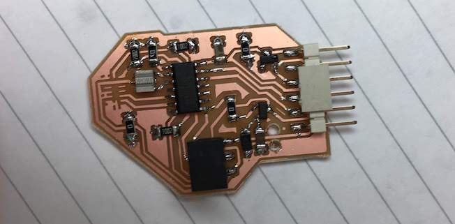
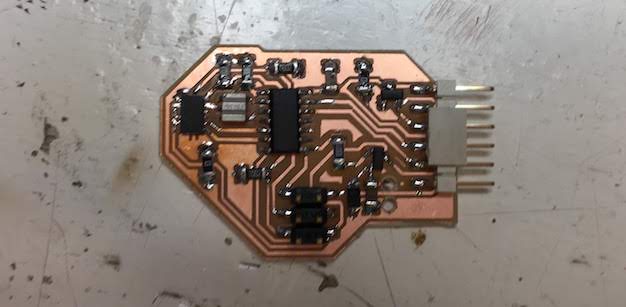
I had trouble with tracing the wires. The accelerometer needed many traces and I switched back and forward many times between the PCB design and the schematic changing dedicated pins and eventually adding multiple 0k resistors to make a working board. Eventually I connected the wrong wires for my accelerometer, but fixed this later by bridging the wires. (I will explain this later)
Due to time constraints I also dropped my nice round design. I save time by letting the board size be determined by an easy to route components order.
Milling
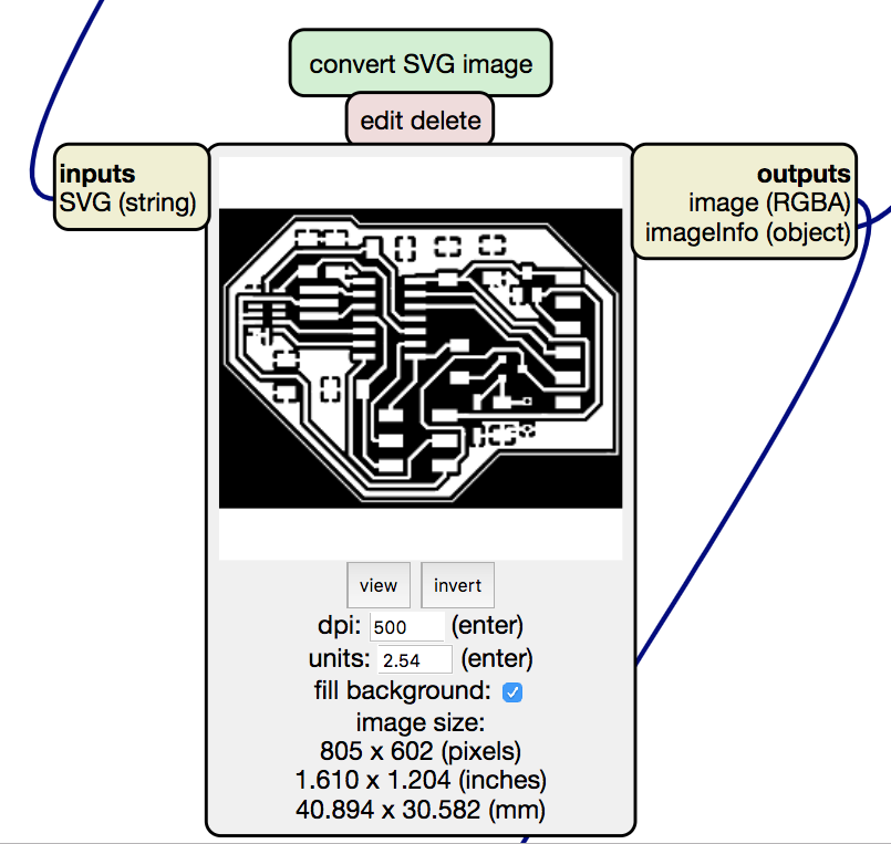
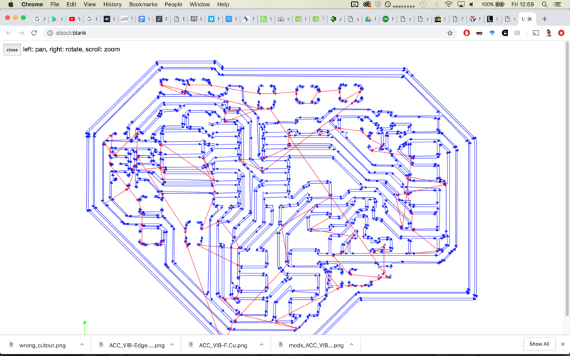
To mill I had to export the PCB design to a PNG.
I actually did not had to export to png, mods now supports SVG for the modella 20x! Yes!
Eventually I still created a png file from each svg, but now using the mods software not the cloudconvert website I used in week7, I first loaded the svg than inverted the image and then viewed the PNG at 500dpi and save it as a PNG.
Also I had to edit the cutout file, since it had a full white lines instead of a white and black field.

For the milling process I took my notes from week 5 as a base.
I did not changed anything to these settings compared to week 5.
The tracelines went really smooth and with no errors.
After the tracelines I took my drill holes for the vibration motor and went through the cutout process. This did work, but gave to large holes (see “Drill holes not matching” fail). Next time I will drill on the inside of these lines.
Besides forgetting to set the correct DPI (see fails “Milling in the air”) the cutout went smooth.
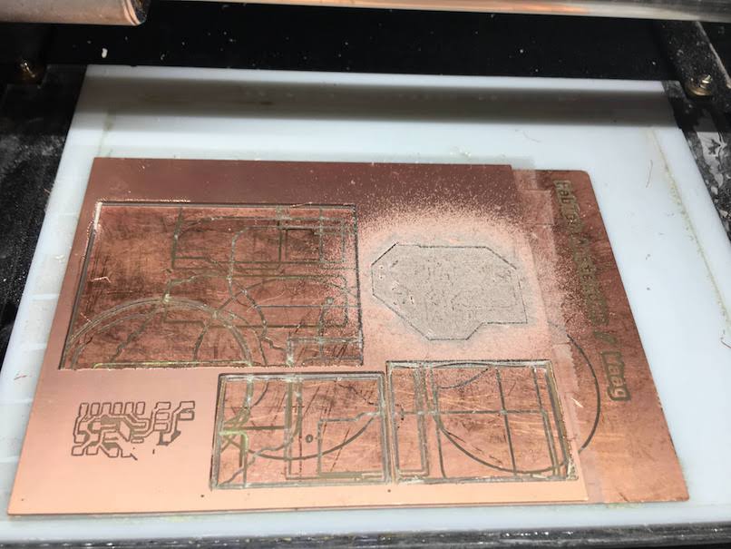
After milling I checked my traces and saw no errors.
Tested basic connections and 3.3V. with voltage meter and it looked all good.
On to soldering.
Soldering
For the general soldering I went through my steps from week 5 for the soldering:
- Remove extra material
- Clean board with soap
-
Find and order components
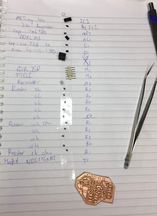
- Solder from inside to outside, from small to large
Heatgun
For small components as the ADXL343 a reflow oven can be really helpfull. It basically works by placing solder on the coper plate using a special mold, gently placing your components, then baking your components to the solder in a reflow oven.
But you can also try to solder using the heatgun.
When using a heatgun you take the following steps:
- Select your components
- Place solder on the copper plate with a soldering iron where you need to solder, try to make it as flat as possible.
- Then gently place your component and try to solder one leg of the component.
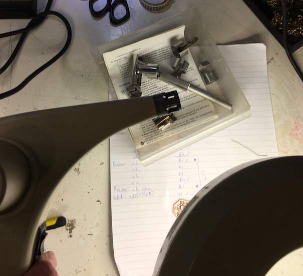
- Take the heatgun and select the proper nozle, I went for the one directing the heat at one point, allowing me to be precise with directing the heat.
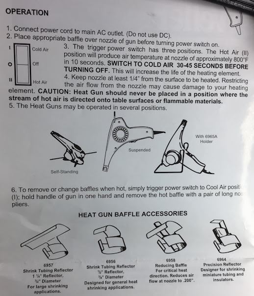
- Place your nozle and turn the heatgun on (setting II, settin I is cold flow)
- Wait a few minutes for the heatgun to warm up.
- Point your heatgun at the parts where you want to solder. Be carefull to not point it to close. This will ruin your components (see fail “Heatgun is difficult”). To determine the correct distance you can first try with some loose solder on a test plate.
- After a few seconds you are done, your components should be soldered to the board.
- Turn off the heatgun and let is cool down before you place it and the nozle back in their proper place
- If possible test to see if your soldering went ok with a multimeter.
Code
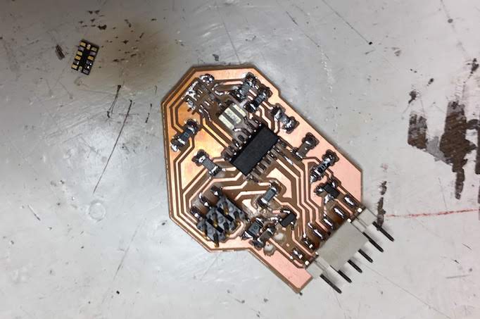
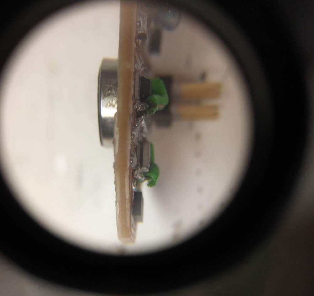
After soldering I burned the fuses (bootloader) and tried a simple sketch to see if everything was working. It was not. I had connected my GND and 3.3V together with a small piece of coper hidden under my SPI. It took me a while to discover this problem. In the process of finding where I had it connected I desoldered and destroyed my accelerometer, and desoldered my 3.3V convertor. Eventually I was able to find the problem, fix it and solder in a new accelerometer with the heatgun. (see also my heatgun fails in the fails section.)
Having a working board I first went on using the vibration motor of week 12, after that I started working on my accelerometer.
I looked at the code from Ilias.
But this is not made for the the ATtiny, it uses the Wire library and Serial.
To convert the code to be ATTiny copatible, I replaced the Serial code for software serial commands.
Next I replaced the Wire code to match with the TinyWireM library of Adafruit.
I installed the library in the libarary manager.
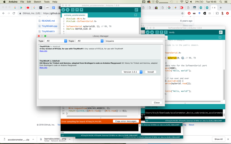
I uploaded the code, and the setup appeared to work, but then I got only jibberish.
maybe I did not select the correct ATTiny connections for the accelerometer?
After looking at the datasheet I saw that I managed to connect the wrong pins to my accelerometer. In my initial design I corrected the right pins, but when trying to optimise my design I changed the pins from the correct deticated I2C pins (PA5 and PA6), I used PA2 and PA3.
I fixed my mistake by bridging the wires.
After fixing the wires I was almost able to communicate with my accelerometer.
Only I was left with 2 problems:
- If I tried to read all 3 axis I got giberish.
- If I tried to read 1 or 2 axis I got a constant number
I first tried to read each axis individual, first x, than y, than z.
All axis kept giving constant numbers, even when moving the device.
I double checked the hex values in the datasheet. These appear to be right.
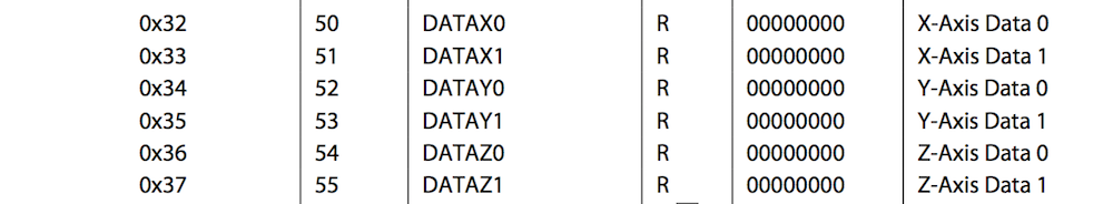
I noticed in the datasheet all axis had 2 registers, so I tried to read both registers for the Z-axis. I still got the constant values.
I further looked at the data I had.
The numbers were different per install, but not per boot, which gave me the impression something went wrong with the installation.
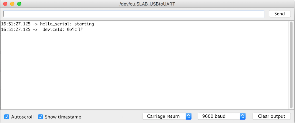
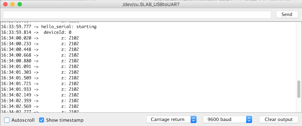
Also I noticed that the DeviceID returned was always 0. According to the datasheet on page 22, this should be the hex number 0xE5, or the dec value 229.
Last the Arduino environment gave the warning:
Sketch uses 3106 bytes (75%) of program storage space. Maximum is 4096 bytes.
Global variables use 191 bytes (74%) of dynamic memory, leaving 65 bytes for local variables. Maximum is 256 bytes.
To reduce the memory load, I replaced the software serial library with the SendOnlySoftwareSerial library I found in week 9.
This reduced my memory to:
Sketch uses 2140 bytes (52%) of program storage space. Maximum is 4096 bytes.
Global variables use 113 bytes (44%) of dynamic memory, leaving 143 bytes for local variables. Maximum is 256 bytes.
I was now able to read the 3 axis, but still had a device ID of 0 and constant axis values.
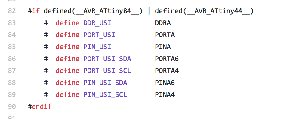
I looked at AdaFruit TinyWireM lib to see if it takes the same pins for the SDA and SDL as I used in my design.
This turned out to be the case. SDA for A6 and SDL for A4. As can be read at https://github.com/adafruit/TinyWireM/blob/master/USI_TWI_Master.h
SDA for A6 and SDL for A4 as defined in tinywirem lib
Henk suggested to check to see if we could talk I2C at al with the chip, by checking if we could find the address. http://fab.academany.org/2018/labs/fablabamsterdam/students/henk-buursen/boards.html
https://playground.arduino.cc/Main/I2cScanner/
Unfortunately this gave the result that it could not find an address.
Henk found that the sda not is connected to the accelerometer chip.
So I tried to fix this by hand soldering the ports again to the chip.
I tried mulitple times, but I kept having that it could not find the address.
Tried again with the heatgun to better connect the pins.
Unfortunately connected the 3.3V and the SCL under the chip, and connected the 3.3V and the second trigger pin.
I removed the accelerometer again with the heatgun, reflowed the solder, and placed the accelerometer back with the heatgun.
Tested again with the testcode, again, nothing found.
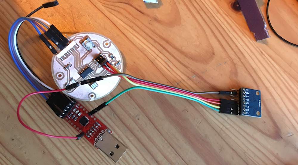
Testing I2C with an external board MPU6050 (accelerometer and gyroscope)
I concluded all hope was lost with the current setup, and I would not be able to get my accelerometer working.
So I went to get an exteral accelerometer board that also uses I2C. If I can get that working, maybe I could later go back to my own accelerometer.
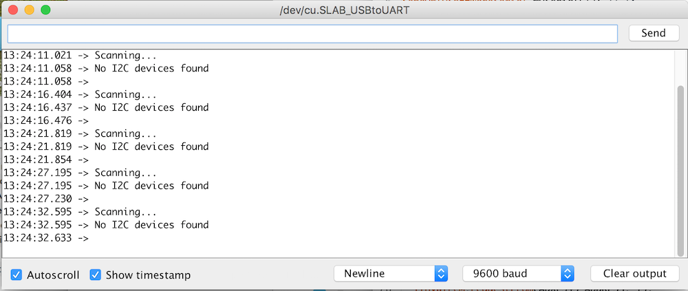
I connected the new accelerometer to my ATTiny using the ISP headers. Ran the I2C test code again, and got “no I2C devices found”.
[foto van setup]
I tested the same setup again, but now with my HelloWorld board, again “no I2C devices found”.
To test if this accelerometer was working, MPU6050, I connected it to my Arduino Uno and ran the Arduino version of the I2C testcode. This offcourse worked!
I2C device found at address 0x68 !
I2CDeviceFound.png Note: the MPU6050 is not only an accelerometer, but also has a gyroscope included.
So my accelerometer was working, only not with my ATTiny, or not with my code.
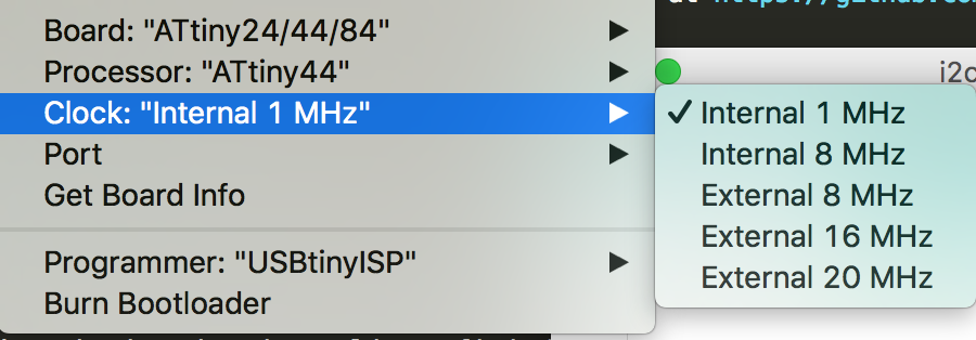
I went back to reading about the TinyWireM library and found a thread talking about the lib only working with an ATTiny at 1MHz, not 8MHz, let alone 20MHz,
So I changed my ATTiny settings to use the internal clock of 1MHz, burned the bootloader and reuploaded the I2C test code.
I tested with both my boards, again, “no I2C devices found”
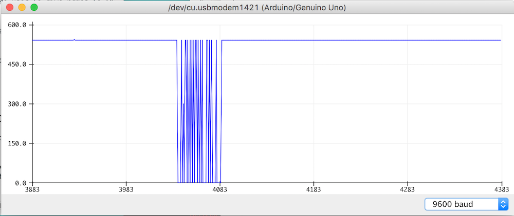
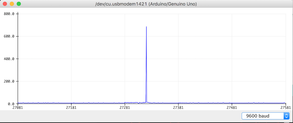
To see if any communication happened on the ATTiny pins at al, I wanted to use the logic analyzer.
At the moment I did not had a logic analyzer available, so I made a very simple version of an Arduino.
I created a sketch to read the Analog pin 4 and send the value over the serial.
Next I plotted the values in the Arduino IDE. This way I could see if something was happening on the lines.
For example, when I connect my A4 pin of my Arduino to the TX of my ATTiny, I saw when the ATTiny was transmitting data:
I connected my Arduino to my computer and used the 3.3V and GND of my Arduino to power my ATTiny board, and to made sure there was a common GND.
When I looked at the SDA and de SCL pins of my ATTiny, I saw nothing. both pins were at a constant value
I was again in doubt if the TinyWireM library was using the correct pins.
I wrote a simple sketch that included the TinyWireM lib and SoftwareSerial to see if I could read the set pins for SDA an SCL.
This gave an error.
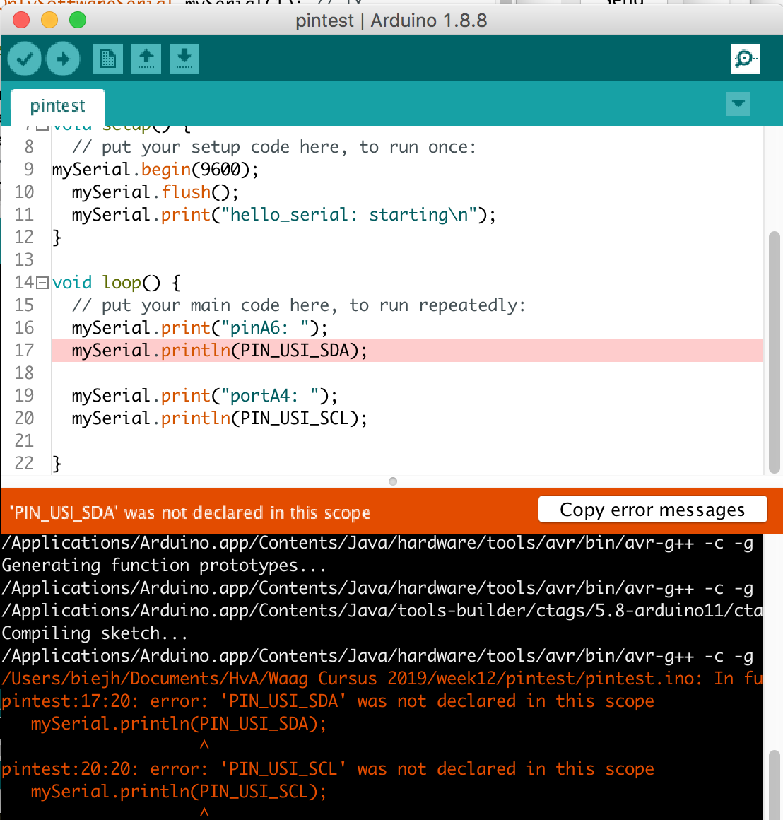
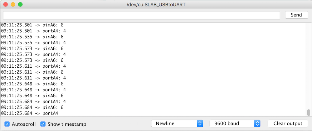
So I redefined the pins in my sketch to see if that worked.
It gave no errors and I was succesfull in printing the pin numers in my terminal.
Pin 6 and 4, so that were the correct pins.
With the redefined pins in my sketch I retried to see if I could communicate with the accelerometer.
But again, no succes.
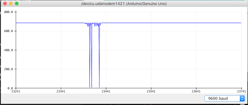
Next I started to play with the code of the TinyWireM lib.
I noticed you can use the TinyWireM.begin() command, but this was not used in my scanning example.
I implemented this in the Setup().
Also I thought that maybe the TinyWireM library does not has enough time to send and receive something back,
so next I send an extra 0x00 byte after starting the wire.
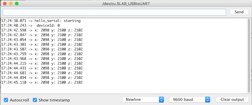
Then I looked again with my analog port on the Arduino, and succes!
We see something happening!
So I can safely conclude that the TinyWireM library does not work when you do not start it with TinyWireM.begin().
This is confusing, since this setting is optional for the Wire library, therefor it was missing in the I2C scanning code.
Having confirmed I am sending and receiving data from the ATTiny, it is time to start trying to communicate with the MPU6050 accelerometer.
Before I try with the ATTiny, I tried to communicate with the Arduino.
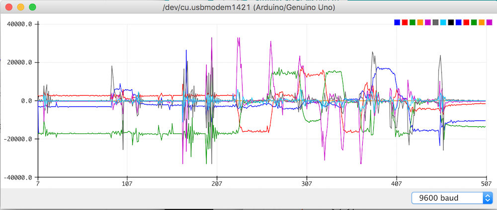
I downloaded an example sketch and plotted the data.
Everything seems to work fine.
I converted the code to work with the ATTiny and used some pixie dust to make sure it would work this time.
And behold! We have a working ATTiny board with an accelerometer attached!
I had some more pixie dust left, so I wanted to give a last try with my ADXL343.
I modified the MPU6050-ATTiny code to work with the ADXL343.
Unfortunately this did not work, my ADXL343 is dead and cannot be revived.
It happends often with the last bit of pixie dust, it is after all mostly dust…
Detecting taps with the MPU-6050
For my final board I use the MPU-6050 that I also used in the input week.
I wanted to use this board to detect taps.
The MPU-6050 does not have dedicated algorithms for detecting taps,
therefor we create a basic implementation on the Atmega using a threshold.
Below the most important snippets, for the full code download TIKTOK micocontroller code (Arduino) with accelerometer, vibration and BLE
struct
{
  byte x: 1;
  int xIntensity;
  byte y: 1;
  int yIntensity;
  byte z: 1;
  int zIntensity;
  long last;
  long current;
} peak;

...

 AcX = abs(AcX);
    xNorm = (AcX * alpha) + (xNorm * (1 - alpha));
    AcX = abs(AcX - xNorm);
    xBuf[0] = xBuf[1];
    xBuf[1] = xBuf[2];
    xBuf[2] = AcX;
    if (xBuf[1] > TAP_MIN_THRESHOLD && xBuf[0]*TAP_SENSITIVITY_LEVEL < xBuf[1] && xBuf[1] > xBuf[2]*TAP_SENSITIVITY_LEVEL) {
      peak.x = 1;
      peak.xIntensity = xBuf[1];
      peak.current = previousRead;
    }

 ...

 //handle peaks
    if ((peak.x > 0 || peak.y > 0 || peak.z > 0) &&  peak.current - peak.last > 50) {
      //tap detected, send package over serial
      int intensity = (peak.xIntensity + peak.yIntensity + peak.zIntensity)/3/100;
      byte pattern[4];
      pattern[0] = intensity;//intensity
      pattern[1] = 0x0A;//duration
      if ((peak.current - peak.last) > 1000) {
              pattern[2] = 0x00;//max pause reached
      } else {
             pattern[2] = ((peak.current - peak.last) / 10); //pause
      }
      pattern[3] = 0xFF;//end

      bleSerial.write(pattern, 4);
      Serial.write(pattern, 4);

      peak.last = peak.current;

      vibrate(pattern);
    }
    //reset peak detection
    peak.x = 0;
    peak.xIntensity = 0;
    peak.y = 0;
    peak.yIntensity = 0;
    peak.z = 0;
    peak.zIntensity = 0;
The code loads a measurement of one axis, in this example the X axis.
Next it makes the value absolute, making sure we only work with positive values.
Then I normalise the value by substracting a running average (the alpha calculation) of the previous values.
Having a normalized X value I store it in a buffer with 2 previous measurements.
Then there is an if statement with peak detection above a threshold.
I compare the 2nd measurement with the first and 3rd measurement and see if it is 8 times higher (TAP_SENSITIVITY_LEVEL).
I determined this sensitivity level by tapping a lot of times on the device and next to the device.
Funny note, without this sensitivity threshold, I would many many peaks when the washing machine is on that is 5 meters away from the table!
So when the 2nd value is higher than the two other values, I count it as a peak, and store this in a struct.
After repeating these steps for the Y and Z axis I check the peak struct if a peak is found.
When found I calculate the average intensity by combining the 3 axis intensity values.
Then I create a package in a byte array containing my new package protocol:
- byte intensity
- byte duration, now default 0x0A (15, what translates to 15x10=150 ms)
- byte pause, either a value lower than 1000 ms or 0
- byte endbit 0xFF
I send this over the software serial to the BLE device, that sends it to the smartphone.
Also for debug I send it to my Serial
To notify the user, I also vibrate the pattern.
Last I reset the peak struct and start the loop over.
Fails
Extra 0 Ohm resistors
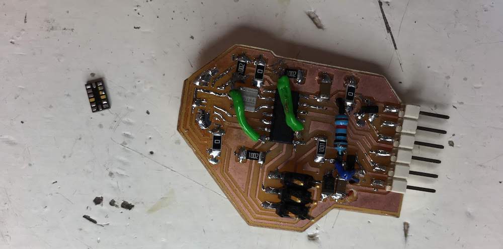
After soldering I was left with some extra resistors. It turned out that during my multiple design sessions of the schematic and layout, I added and removed components. In stead of reanotating the existing components, I only annotated the new components. It appears that KiCad does not detect that the components that are not used and removed do not exist anymore, and it keeps them in the part list.
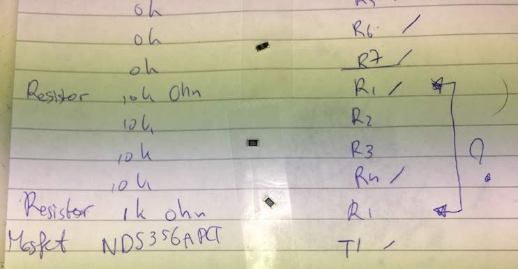
0kOhm instead of 1kOhm on the board
At the end of soldering I had a 1KOhm resistor left. It turned out I had soldered a 0k resistor instead of a 1k resistor. I replaced the resistor, see the pictures for the difference.
Connecting the wrong wires
As explained in my main section I switched back and fort many times between my PCB desing and schematic to change pins to make tracing the wires easier.
In the end I change my SDA an SCL pins of my accelerometer to different pins on my ATTiny.
Big mistake! It took me some time to find this problem, and I had to bridge the wires or mill a new board.
Since this was the only accelerometer left, I had no choice but to keep trying with the current accelerometer, so I had to bridge the wires.
I did not had nice small wires, but managed to bridge it in the end.
Out-of-time (to complex)
Designing my first board in week 7 took me less time than I anticipated, I expected this time to also be an easy process.
My mistake, because I had used (alsmost) all the pins of the ATTiny, routing was way more difficult. Also I wanted to keep the round shape, to work towards my armband design.
After 4 hours of tracing wires and still not finished, I decided to drop the round design, and just see how big my design will be.
This solved many problems and after two hours and 2 extra 0K ohm resistors, I had a finished strange shaped design.
Heatgun is difficult
During the soldering and desoldering with the heatgun I destroyed my traces and the accelerometer.
I learned that it is really difficult to get the correct distance with the heatgun for making your solder liquid, but not destroy your components.
I had to resolder a new accelerometer and I made sure to keep my distance, it took me longer to solder the component, but I did not destroy it.
Heatgun and too little/much solder
During the debuggin of my accelerometer I had to multiple times solder and desolder the accelerometer with the heatgun.
Once I placed to little solder at some points, therefor not all pins were connected.
The next time I placed to much, making pins connected to eachother.
It was really difficult to determine the correct amount of solder to apply to let the heatgun melt it and the component to be connected, and I think by the time I managed to correctly solder with the heatgun my component was destroyed.
Reflection
It is amazing how many things went wrong (desing, soldering, heatgun, code), and how difficult it is to determine what actually went wrong.
Next time I will make sure I have access to a logic analyser when debugging my work,
also I will make sure I have enough spare components, for when something goes wrong: the new aim is to have 3 of each.
Also next time I will stay away from the heatgun and try to either use a reflow oven, or larger components.
Still I am happy I was able to determine that it is possible to use the ATTiny44 and the TinyWireM library with an accelerometer, even if it is not the device I had soldered and destroyed on the board.