Week 7: Electronics design
03/05/2019 - Stéphane Muller
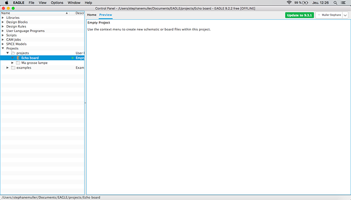
As a group we have to use the test equipment in our lab to observe the operation of a microcontroller circuit board. Individually we have to redraw the echo hello-world board, add (at least) a button and LED (with current-limiting resistor), check the design rules, make it, and test it. Extra credit: simulate its operation and render it.
We've had some practice with Eagle during our training with Adel before the Fab Academy, so designing the board shouldn't be too hard. If I have time I'll try KiCAD later.
Research
Some interesting ressources for this week:Planning and list of tasks
- Designing the board on Eagle
- Adding the button and the LED
- Making the board
- Testing the board and observing the operation of an MCU
Step by step
Group assignment
Check out our group documentation.
Designing the board on Eagle
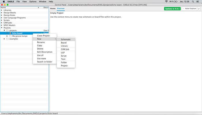
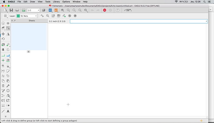
The first thing you need to do when you open Eagle, is create a project and then a new schematic.
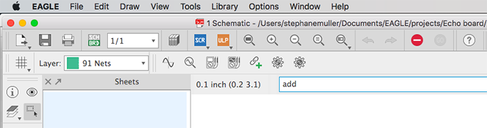
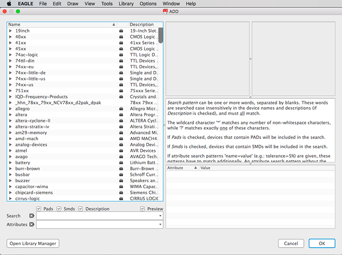
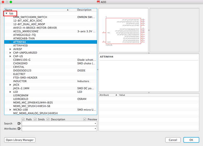
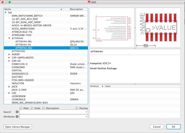
Then you need to go shopping for all the components you'll need. To do that, I typed the Add command. This opens up a dialog box with a very loooooooong list of components. In there I went looking for the "fab" category. It's the list of components of the fablab inventory. I had installed it prior to the Fab Academy, during our week with Adel. When you select a component, you can still choose between different versions of the same component. It's mainly a question of size. We're using 1206 SMD components. On the right of the dialog box you get the footprint of the component on the board.
Once you have all your components, you link them together. You can do one giant plate of spaghetti with links going all over the place... or you can name the end of some links and refer to them on other parts of the schematic. When you do that, Eagle will ask you if you want to connect those links together.
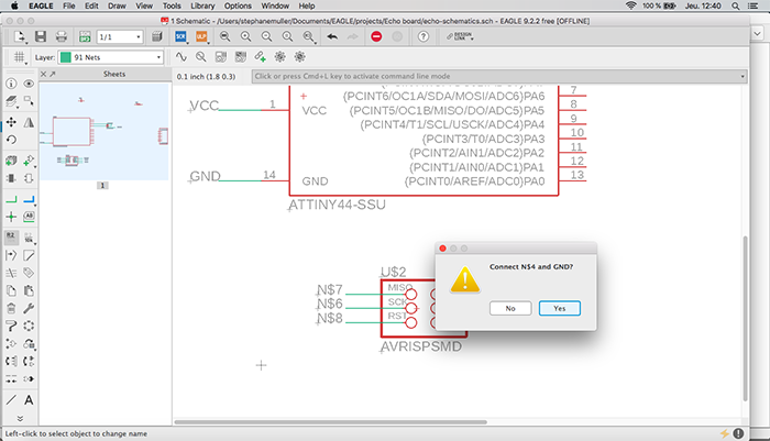
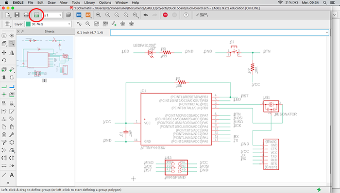
Once I was done with the basic schematic, I moved on to adding the button and the LED.
Adding the button and the LED
To add the button I used what I learned in the tutorial on pull-up resistors. Basically you need to connect one pin from the ATTiny to Vcc with a pull-up resistor in between, otherwise it creates a short and the ATTiny will overheat from drawing too much current. The resistor is here to limit the current (Ohm's law is your friend). Then you connect the pin from the ATTiny to the button as well and the other part to the ground. That way, when you press the button, the ATTiny pin is shunted.
What all this means is that, when the button is open, the pin will have a HIGH voltage and when the button is closed, the pin will have a LOW voltage. And the difference between the two voltages is significant enough for the ATTiny to differentiate.

As for the LED, well, that was easy enough... you just connect a resistor first, (once again) to limit the current, and then the LED, with the arrow (the anode) pointing to the ground.
An easy way to remember to what side anode and cathode refer to is that there is a "N" in anode and that's the negative part.
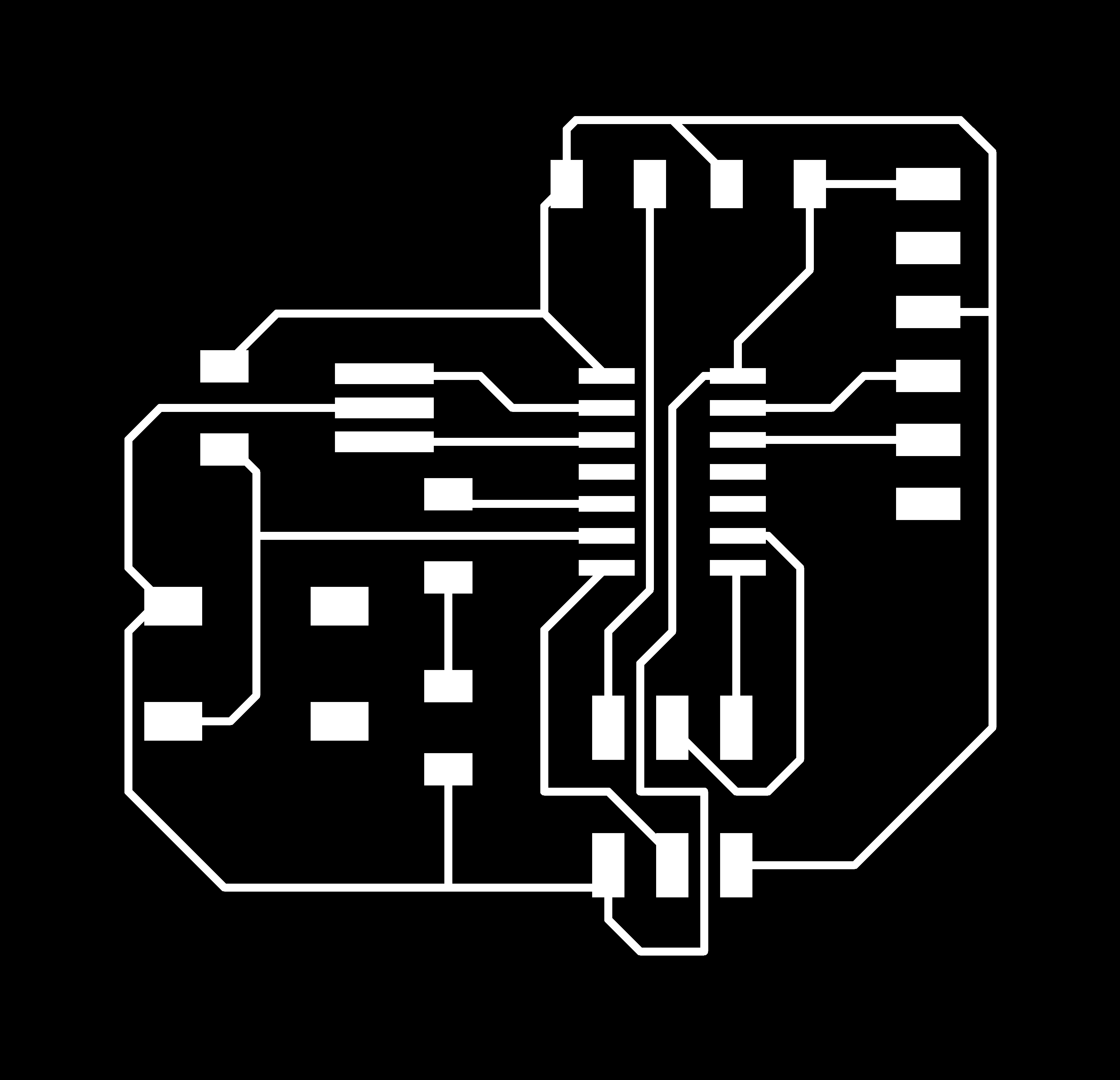
And here is the final schematic! Now we just need to click on the button showing SCH/BRD (top left of the screen) to switch to the board design part.
When you get to that part it's a joyful plate of spaghettis...
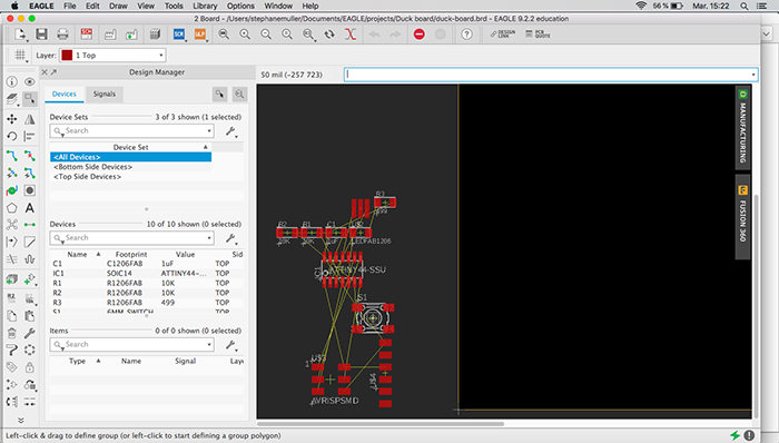
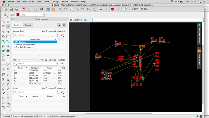
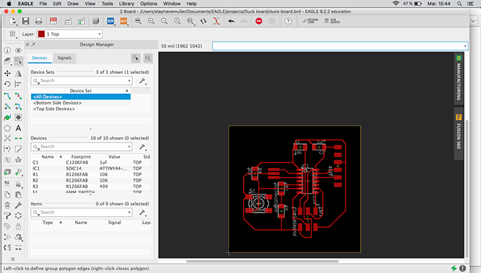
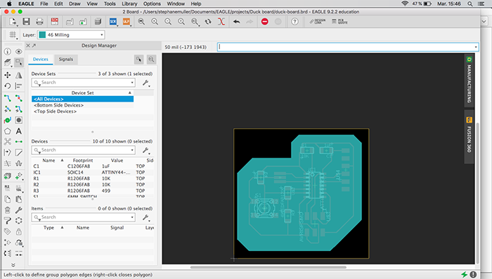
So the first thing is to try and place them closest to the parts they're linked to. Here it's relatively easy because we can copy the original board's parts placement (minus the button and the LED). But generally I would think it's a good idea to put the ATTiny (or the MCU) in the middle and the ISP module right under it.
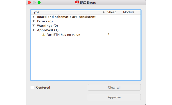
Checking the electrical rules (ERC) is also very important. Here you can see the flaws in your design. In mine for example, it says the button component has no value (which is not important) and that there are routes without a destination. I put a wire at the end of all the ATTiny's pins without wiring all of them and he didn't like it.
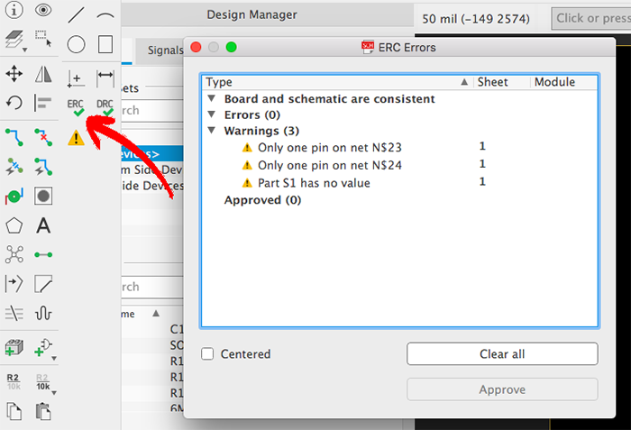
I removed the useless wires and approved the warning and now it's OK.
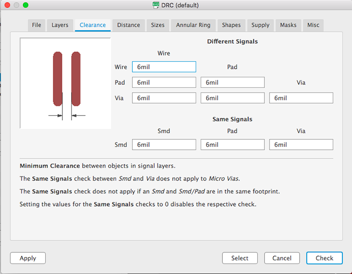
To set the design rules for the board, you need to click on the DRC button in the tool panel. Here are the design rules I used.

Then comes the fun part of finding the right paths for every connection. As I said, here it wasn't that hard, thanks to the original board, but placing the LED and button still required to use 2 resistors as bridges for other paths. Here is the final result:
Once you're done arranging parts, you need to draw the outline of the circuit board. To do that you go to the milling layer and use the polygon tool to draw the shape you want.
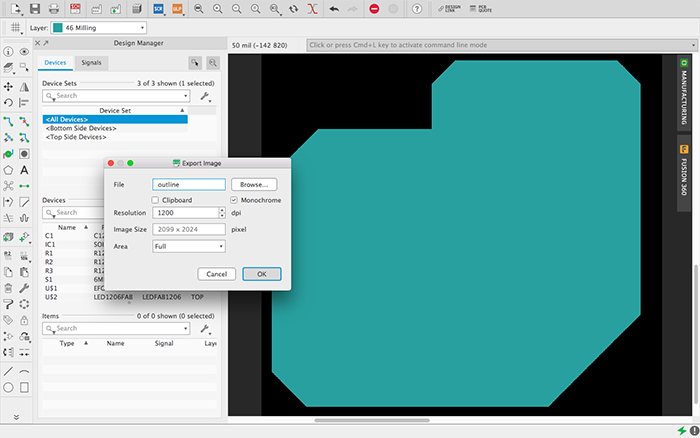
Final thing you have to do is export the traces and the outline as images for milling. To do that, first you need to show only the layer you want to export, like so:
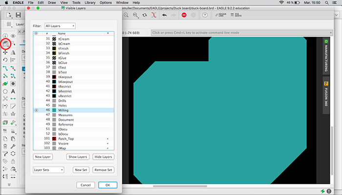
And then go to File > Export > Image. Increase the resolution, check the monochrome option and save the file. Do this for the traces and the outline.
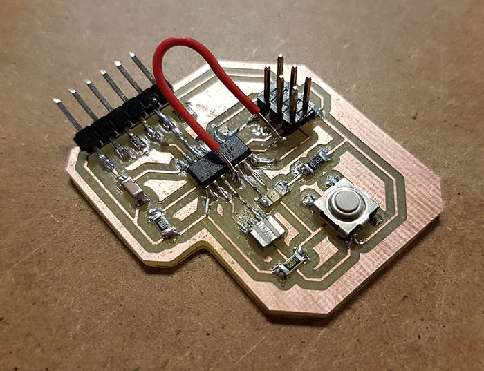
Making the board
To make the board I used the same production process as 2 weeks ago.
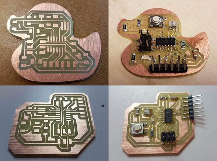
However, I ran into problems during the tests. I tried to upload Neil's code and it wouldn't work. I kept getting errors like Invalid Device Signature or initialization failed, rc=-1. So I checked and re-checked my connections like a million times... adding soder, cleaning what I could, making sure everything was OK, testing with different programmers and computers... but nothing gave. So Tuesday, in the face of despair, I started all over (design on Eagle included). I shaped the first version of my board like a duck. I loved that duck, it had 2 LEDs. But when I started over I decided to keep it as simple and as close to the example as possible.
Testing the board and observing the operation of an MCU
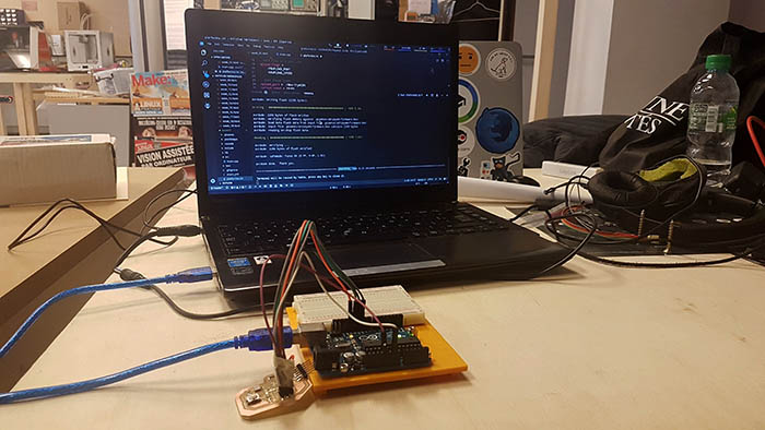
I had a lot of trouble testing the board... even the second version gave me headaches. It wouldn't work either and I got VERY frustrated. I was banging my head against the wall. So when week 8 began and my board still wasn't working, I thought: "let's put this aside for now, we'll get back to it during week 9".
So here we are, this time I really have to make it work. I was getting ready to make a new board, but since my second board seemed fine, I thought I would check my Eagle file. So I compared my board to Neil's to make sure everything was in order and I didn't miss anything obvious. Bingo... the reset pin on the ATTiny wasn't connected to anything. So I made a bridge between the ATTiny's pin and the ISP's reset pin.
As I had a lot of trouble programming with my own computer and I just wanted to make sure the board was working, I asked my comrade Leo if I could use his computer and his Arduino to do it since I knew his configuration worked. And low and behold... it worked!!
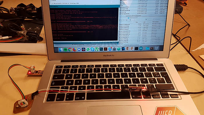
The LED did not shine very bright. My initial thoughts were that there might be a voltage divider somewhere or a bad connection. After some investigating and knowledge that only came afterwards, it turns out the LED wasn't declared as an output in the code. The blinking still works but at a much lower voltage.
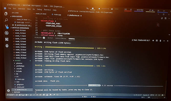
Later I was even able to programm it with my own computer and my FabISP (we're in week 17 and the FabISP works perfectly, it has not let me down).
The FabISP only works if you provide your board with a second source of power...
Conclusion
This assignment was a LOT more challenging than I thought. I ran into quite a few bumps. It's a bit ironic since the circuit was quite simple and I didn't have a single problem when doing the FabISP... Silver lining is I learned a lot while debugging my board and I'm proud I found the issue.