
Fab Academy 2019 - Lucas Lim
07. Electronics Design
07. Electronics Design
Group assignment:
Individual assignment:
I am new to the world of electronics and this week is my second lesson on electronics. I am thankful for the teaching and guidance provided by my Fab Lab instructor, Mr Steven.
This week assignment involve designing the "hello-world board", which include drawing of the schematic as well as broad diagram, PCB fabrication, stuffing the board and lastly to test the board to see if is working or not. Two components are added, one is the button (switch) which will be used as an "input device" and the other is a LED which represent an "output device".
The workflow is as follow :
This week learning journey includes :
- using EAGLE to draw the schematic
- base on the schematic, using EAGLE to draw the board design
- reading up on basic concept of electronics, circuit design
- reading up on the physical components (ATTiny44 microprocessor, resistor, LED diodes, etc)
- PCB fabrication
- ways to test the board
- programming the board
- learn using the linux command "convert" to mass convert and resize my photos
- learn html/css code to create a photo gallery style to display my photos
I am using the academic version of Autodesk EAGLE (version 9.3.1) to draw my schematic and board design for my "hello-world board", as EAGLE is free for academic use for up to 3 years, iEAGLE is user friendly, and include an integrated schematic editor and board editor. However, the academic version has a limit on the board size.
Reference :
Autodesk EAGLE website
Electronics core concept :
Electricity is the flow of electric charge (or electrons). In order for electric current to flow, there must be an electric potential difference, a close-circuit and a conductive material (like copper).


Reference :
Voltage, Current, Resistance, and Ohm's Law
Schematic Design :
Designing a schematic is the very first step in PCB design. A schematic drawing can be refer to a blueprint for making our circuit board in the Fab Lab. It is a drawing representing a circuit, symbols to represent real-world electronic components, lines representing "traces" or electrical path which connect all the components together.
Reference :
Fab Academy Tutorial : Introduction to Eagle
SparkFun Tutorial : Voltage, Current, Resistance, and Ohm's Law
SparkFun Tutorial : Electricity Basics
SparkFun Tutorial : EAGLE PCB Design
SparkFun Tutorial : How to Install and Setup EAGLE
1. Downlaod the Fab Lab library named"fab.lbr" for EAGLE from class site. In GitHub repo, there are other fab lab libraries available, but they are a subset of the main "fab.lbr"
2. I placed the file "fab.lbr" into a newly created folder call "fab_lbr" in the EAGLE directory (C:\EAGLE 9.3.1\fab_lib), as I do not wish to place the fab lab library into EAGLE default path $HOME\EAGLE\libraries.
3. At EAGLE Control Panel, go to Main Menu -> "Options" -> "Directories", add in the fab lab library directory name ";$EAGLEDIR\fab_lib" behind the default EAGLE library path.

4. I am not using the default EAGLE library as EAGLE's thousands of library files can be overwhelming, or more than I ever need, so I hiden them for the time being. I went to EAGLE Control Panel, at the left side panel, under EAGLE "libraries" category, select EAGLE default library “Libraries”, right-mouse-click and select "Use none"

6. I selected "fab.lbr", right-mouse-click and select "Use". A big green dot next to the library indicate that it is in use. You could also turn-on other libraries, like "frame.lbr" from EAGLE, or libraries from SparkFun, etc

7. Create a new schematic file :
At EAGLE's Control Panel, I created a New Project called "hello_world" which will store both my schematic and board design. Right-mouse-click on the project name and select "New Schematic"
8. Configure EAGLE User Interface to your personal preference :
I changed the background colour from white (default) to black colour as a black background will be easier for my eyes and it easier to see the highlighted symbols.
9. Next I turned on the grid display a set the size of grid size to a smaller 0.05 for easy placement of components.

10. Identifying the components :
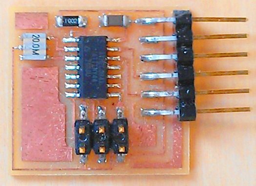
By looking at Prof. Neil's Hello World board, you can easily identify the various "surface mounted" components on the "single-sided" board.

11. Adding/placing the symbols in schematic :
Type the "add" command in EAGLE's command box at the top. At the Add component windows, searched for the "ATTiny44" microcontroller in the Fab Lab ibrary, and add to the schematic.
The search function in EAGLE is very literal, example if I search for "ATTINY", there is no result found, however if I use "wildcard" and placed an asterisk (*) before and/or after my search term, I am able to find the ATTiny44 chip.
I continue to add in the other components.


Some bacics EAGLE commands :
Using shortcut keyboard command is sometime faster than moving the mouse and click on the icon at left tool panel.
Moving/rotating the symbol :
Each symbol (including the label on the Net connection) has a small crosshair in the center of the symbol which represent "the centre of origin". Clicking on the crosshair allows for easy selection/moving. Use the MOVE command to move the symbol into the desired position. To rotate an object, simply click on right button of mouse.

ATTiny44A
There are a few open pins (or floating pins) available on the ATTiny44A microcontroller, namely PA2, PA3, PA7 and PB2. Therefore I used the open PB2 to connect to the LED, and the open pin PA7 to connect to the S1 (Switch).

Reference :
ATTiny44A datasheet
LED Diode
A resistor is needed to prevent the LED diode from blowing or "over-current". The supply voltage (example from the USB cable) is "5V", and will run the red LED at a forward current of 10mA. As the same current will flow through the circult, a "pull-up resistor" is commonly used and placed in between the VCC (supply voltage) and the LED.
V = Voltage in volts
I = Current in amps
R = Resistance in ohms
Using Ohm’s law :
V=IR, therefore
R=V/I
R=(V(Supply Voltage)- V(LED voltage drop)) / I
R=(5V - 2V) / (0.01 A)
R= 300 ohm
So, I used a 499 ohm resistor as it is ok to have a slighly higher value resistor for LED.

Tip : You can set attributes on the component in EAGLE by clicking on "attributes tool" icon or by right-clicking the componenet origin and selecting attributes from the popup menu. Eg. Create new attribute for LED like "Color"
LED Resistor Calculator Online
An online LED Resistor Calculator @ https://www.allaboutcircuits.com/tools/ that I used too.

Capacitor
A capacitor is used to store an electric charge. But the capacitor used here is quite small and as such is not polarized. The 1uf capacitor is placed after the voltage supply and before the resistor and microcontroller to act as a filtering of pulses. As voltage enter the capacitor, the capacitor charge up and store the pulse voltage, and then it dischages out and maintaining a smooth and constant DC voltage flow.
My components list :
| # | Label and value on Hello World | Part Description | Part Library | Part Name | Quantity |
|---|---|---|---|---|---|
| 1. | IC1 - t44 | ATTiny44 microcontroller (surface mount) | Fab Lib | ATTINY44-SSU | 1 |
| 2. | R1 - 10k | Resistor 10k | Fab Lib | RES-US1206FAB | 1 |
| 3. | R3 - 10k | Resistor 10k | Fab Lib | RES-US1206FAB | 1 |
| 4. | R2 - 499 | Resistor 499 ohm (for LED1) | Fab Lib | RES-US1206 | 1 |
| 5. | C1 - 1uF | Capacitor | Fab Lib | CAP-US1206 | 1 |
| 6. | JP1 - ISP | 2 x 3 pin header | Fab Lib | PINHD-2x3-SMD | 1 |
| 7. | JP2 - FTDI | 1 x 6 pin header | Fab Lib | FTDI-SMD-HEADER | 1 |
| 8. | RESONATOR - 20 MHz | Resonator | Fab Lib | Resonator (3-pin) | 1 |
| 9. | S1 | Switch | Fab Lib | 6MM_SWITCH6MM_SWITCH | 1 |
| 10. | D1 | LED diode | Fab Lib | LEDFAB1206 | 1 |
| # | Label | Part Description | Part Library | Part Name |
|---|---|---|---|---|
| 11. | GND | Ground symbol | SparkFun Lib | GND |
| 12. | VCC | VCC symbol | SparkFun Lib | VCC |
12. Connecting the components :
Use the "NET" command to connect up the pins of the various symbols/components on the schematic; by howering the mouse cursor over the very end of the pin and click to draw a line (Net connection) to the pin of the component that you wish to connect.
Do not use the "WIRE" command to connect components, "WIRE" command is better-meant for drawing lines.
To keep my "Net" connection tidy and neat in some area, I drew a short "Net" connections sticking out from the end of the pin. This is known as "Net Stubs". Then used the "NAME" command to name each of the Net Stubs. The LABEL Tool can also be used to aesthetically display the label on the Net Stubs.
Note :
Make sure that the orientation of the component is correct, like the FTDI connector pin 1 (GND) is facing upward.
CTS and RST pins on the FTDI connector are unused.

13. Checking the schematic
Use the "SHOW" command and select a "Net Stub" connection allows you to visually inspect the end-to-end connection to make sure the link is correctly established.

Electrical Rule Check (ERC)
After visual checking my schematics, I clicked on the ERC Checker Tool (which is located at the side panel in EAGLE Schematics Editor) to check my schematic for any error.
The ERC will check for :
1) Are all of your nets properly connected
2) Do you have any conflicting outputs/inputs on your schematic?
3) Are there any open or overlapping pins and ports on your schematic?
ERC has three types of errors :
Consistency Errors: error between the schematic and the board design
Errors: Serious error that need to be addressed, like OUTPUT pin and SUPPLY pins mixed up, etc
Warnings: warning, but these will not mess up your circuit
ERC shown one warning relating to a missing value for S1. As I am using a 4-pins switch, and the other two pins are isolated and not connected to anywhere, so it is ok. I selected the warning and clicked "Approve" to confirm that I had 'understood' the issue and prevent the notification from popping-up again in the ERC checking process. The 'approved' issue will appear under 'approved' section at the bottom of the ERC screen the next time you run the ERC again.


14. Finishing touch to schematic design
I used the "ADD" command and added an A4-size frame from SparkFun library.
My 'Hello World' schematics :

Note : I tried to position the components accordinly to the way that I think I would place the physical components on the actual 'hello world board' with FTDI connector on the right, ISP 6-pin connect at the bottom. LED and Switch (S1) on the left. In future, another way might be for me to place on the 'input' devices on the left and 'output' devices on the right.
Files :
My Hello World Schematics (hello_world.sch)
15. Generate a new board design
Click on the "Generate/Switch to Board" Tool to generate a new board design based on your schematic.

16. Resize the board size
Use the "MOVE" command and click on the corners of the black-colour board space and resize to closely resembling of the actual pcb board size (FR1 : 2 inch x 3 inch) that you going to be milling. Take note to draw your board or place all your components as close as possible to the bottom-left corner where the small crosshair is.

17. Display and setting the grid
I enabled "Gridline" display and set grid style as "dot" and gridlines distance to "25 mils" for easy placement of parts and drawing of the routes.
All the parts will be shown and connected to thin gold lines which are called "Airwires" and require the use of "ROUTE" command to convert them into "traces" for the PCB. At times when I need to squeeze in a route in-between two pads, I will hold down the ALT key on my keyboard to access the alternate grid, as defined in the "ALT" box in the Grid screen.
18. Placing the componenets
I clicked on the "layer" tool and hide some layers that I do not want to see, for easy placement of the componenets.

I placed the switch button at the bottom-left corner, opposite the FTDI connector, as it be easiler to press the button.
19. Drawing the route
Set layer to "Layer 1 - Top", set the "wire bend" style to be "90 degree" bend and width to be "12" mil.

I drew the routes, starting with the shortest "airwires" first. Using the "RIPUP" command to erase route occasionally and redraw.

20. Drawing outline and text
I drew a square for the outline on "Layer 46-milling". Important to take note that the 6-pin FTDI header require some space for support, so I drew my outline on right side a bit further distance away from the FTDI header.
I added in some text (my name and "hello_w") to be engraved onto my board. Need to change the font type from "proportional" to "vector" graphics for engraving text.
21. Checking of Board Design : EAGLE DRC
I ran EAGLE DRC (Design Rule Check) tool to check my board against the current set of Design Rules. It is a best practice to make sure that the trace should be wide apart to have some tolerance during the (CNC) machining etching process, like cater for spindle runout.
Consideration :
I am using a 0.1mm 10-degree angle v-bit at 0.9mm depth (Z-down). I drew my 'Net' in 12 mil which is about 0.3048mm which is a bit wider than the default 6 mil. I prefer a wider trace width, as it will not easily be peeled off when you doing sanding or soldering, etc.
For a new beginner in electronic production, I had set the Minimum clearance to 16 mil for wire-to-wire, wire/pad-to pad instead of using the default 6 mil which is too narrow (default 6 mil is equal to 0.1524 millimeter). The v-bit tend to cut a bit wider than a flat end mill, which allow me to run with just a single pass.

The DRC Check had detected some 'clearance' issues. I ran through each 'clearance' issue by clicking on each of them and then retified it by shifting the affected 'trace(s)' to create more clearance space in-between them. This will clear the 'clearance' issue in EAGLE DRC when you do the DRC scan again.


I saved the setting to my own Design Rules file call "Lucas.dru", so that I can load this file for DRC in the future.
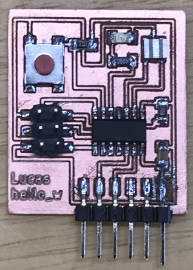
22. My board design :

Files :
My Hello World Board (hello_world.brd)
23. I run the pcb-gcode ULP to convert the board to gcode. I selected single pass as I be using a 0.1mm v-bit which tend to cut a bit wider.
(Please refer to my week 5 - Electronic Production for detail explanation on PCB fabrication).


Files :
hello_world.top.etch.gcode
hello_world.outline.gcode
24. I used "CAMotics" to test out my two gcodes (one for traces, the other for outline) to look out for any problem area or error with the gcode.

25. Milling the hello world board and stuffing the board :


I am using the "Sanwa CD800a Portable Digial Multimeter" which is available in the fab lab to test my circuit board. This was my first time doing so and this process is a very important step in electronics so as to avoid damage to your PC/notebook as well as the circuit board when you plugged in a live current to the circuit board and connect to your PC/notebook.
I used a digital multimeter (DMM) to test my circuit board
- after I finished soldering each component on PCB
- and one final check after I stuffing my 'Hello World' board before I connect to a power source

Testing 'Continuity' on the circuit :
What am I testing? : The VCC (Supply Voltage) path that ensure that power is able to reach various part of the circuit. Vice versa, the GND path should be one circult by itself. The individual path of travel by the current should not cross over to other path(s) like the path from each connected I/O pin on the MCU to the pin on the connector. and etc...
1. Take out the two test probes (or sometime called leads) from the side compartment.
(Note that for some other model of multimeter, there are a number of different ports and you have to insert the Red probe into 'mAVΩ' port (for measuring mA, Voltage or Resistance) and black probe goes to 'COM' port(which is Common port or connect to 'Ground'))
2. Turn the big FUNCTION knob to point to  which look like a 'buzzer' icon

3. Press the SELECT button to point to
4. Apply the tip of the red and black test probes (at the tip of the test lead) to a circuit to measure.
Example place one probe on the pin of the ATTiny44A and the other on the copper track where that particular pin rest.

5. This is to test for continuity, if there is current flow or continuity in the circuit path, the buzzer will sound. If not, solder joint might be a cold joint, "re-work" is needed.
--------------------------------------
6. Testing for spilled-over solder :
Remove the probe from the pin and now place on the adjacent area/copper track next to the original copper track. The other probe is still resting on the copper track. We should not hear the buzzer sound, the display on the DMM will show an 'OL' for 'Open Loop' or 'Open Circuit'. If the buzzer sounded, that means there is a "short" and current is flowing to adjacent area or track; meaning some solder has been spilled into the gap. 'Re-work' is needed.
--------------------------------------
7. Lastly test for "short" of VCC and GND. There should be no buzzer sound.
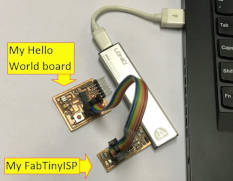
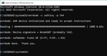
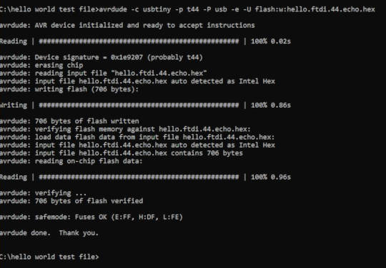
1. I connected my Hello World board to my ISP/Programmer. I am using my FabTinyISP which was fabricated in week 5 - electronic production. I ran the command "avrdude -c usbtiny -p t44". AVRDude is able to detect the ISP as well as the target board (hello world) successfully. The avrdude command also ensure that the devices are supported (correct firmware).
avrdude -c usbtiny -p t44
Syntax : avrdude -c {programmer : eg. usbtiny} -p {AVR chip on target board : eg. t44}
2. Download the hello world test file "hello.ftdi.44.echo.c" from class site.
3. Programming overview :
4. I follow the steps mentioned on the "Setting Up AVR-GCC toolchain and avrdude To Program An AVR Development Board In UBUNTU" website. You will need the following :
- ISP (that we made in week 5 - electronic production)
- hello world board (that we fabricated this week)
- ISP 6-pin (2x3) cable
- avr-gcc (software) : avr-gcc is a GNU C cross-compiler for specifically for AVR
- avrdude (software) : avrdude is a utility that transfers codes from the PC to the AVR microcontroller.
At the command prompt in Windows, I ran the following commands :
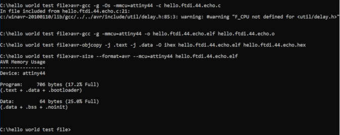
avr-gcc -g -Os -mmcu=attiny44 -c hello.ftdi.44.echo.c
//generate .o file
avr-gcc -g -mmcu=attiny44 -o hello.ftdi.44.echo.elf hello.ftdi.44.echo.o
//generate .elf file
avr-objcopy -j .text -j .data -O ihex hello.ftdi.44.echo.elf hello.ftdi.44.echo.hex
//generate .hex file
avr-size --format=avr --mcu=attiny44 hello.ftdi.44.echo.elf
(The microcontroller name is: "attiny44" (guide to "avr -mmcu option", filename is "hello.ftdi.44.echo.c")
Transfering the .hex file onto the (hello world) board.
avrdude -c usbtiny -p t44 -P usb -e -U flash:w:hello.ftdi.44.echo.hex
Result is ok.
Reference :
Setting Up AVR-GCC toolchain and avrdude To Program An AVR Development Board In UBUNTU
This week lesson continues from week 5 - electronic production and is on the topic of electronics. It is quite tough for me as I need time to take in all the information taught in class as well as by our local Fab Lab instructor. I also made a ccouple of mistake and it slow down my progress and made me a bit frustrated.
I spend two days to learn EAGLE, to draw the schematic, follow by the board design. EAGLE user interface is user friendly and after a while I get used to it.
One whole day in pcb fabrication and soldering. Follow by reading up on AVR Programming and how to program my hello world.


Make File :
Installed with WinAVR is the "Make" utility and the "makefile" template, it is a bit overwheliming for me to learn how to make use of the Make utility. In the future if I have some spare time, I might explore on this and simplified the compiling and uploading of my code.
WinAVR is an extremely old software and the development of WinAVR has stopped. In the future, might have to look for other latest software to replace WinAVR.
In conclusion, once you overcame the initial fear of electronics as well as the frustration in failures, and grow more and more knowledagable and exprienced, electronics can be a fun thing.
My Hello World Schematics (hello_world.sch)
My Hello World Board (hello_world.brd)
hello_world.top.etch.gcode
hello_world.outline.gcode
ATTiny44A datasheet
Fab Academy Tutorial : Introduction to Eagle
SparkFun Tutorial : Voltage, Current, Resistance, and Ohm's Law
SparkFun Tutorial : Electricity Basics
SparkFun Tutorial : EAGLE PCB Design
SparkFun Tutorial : How to Install and Setup EAGLE
SparkFun Tutorial : Pull-up resistor
Schematic Basics Part 3: ERC
Create g-code from EAGLE file
KiCad website
Arduino website
Setting Up AVR-GCC toolchain and avrdude To Program An AVR Development Board In UBUNTU