
Fab Academy 2019 - Lucas Lim
05. Electronics production
05. Electronics production
Group assignment:
Individual assignment:
This week assignment is to fabricate our very own ISP (In-System Programmer), hereby called the "FabISP", which means "Fab(-able) ISP". So instead of buying a commercial ISP, we can fabricate a simple USB ISP in the FabLab which will
cost just a
few dollars. This FabISP which will in-turn be use to program the microcontroller(s) on our electronic boards that we going to be making.
This week assignment is not to "design" the ISP but use one of the "pre-defined" designs from the Fab Academy class site. I followed
Brian's FabTinyISP tutorial from the class site and using his design.
I am new to electronics, and it took me some time to understand about basic electronics (all the terms, components and etc), soldering, staffing the PCB and programming.
This week learning outcome is to get familiar with PCB and the PCB fabrication process, which include the following :
- PCB software : like mobs and Autodesk EAGLE software
- basic of electronic circuit design, traces, pads, etc
- PCB fabrication process : what is gcode, basic of PCB (CNC) milling machine, what is CNC (which stands for Computer Numerical Control), type of end mills and v-bits to use, material of PCB board, etc
- "stuffing" the board which is the process of placing the componenets on the board
- types of SMDs and soldering SMDs (surface mount devices)
- testing circuit with a digital multimeter
- programing and testing the FabTinyISP
ISP refer to "In-System Programmer". In simple term, it is explained as an USB device that seat between the computer and your target board (the target board is with the AVR microcontroller chip that you would like program upon). It main purpose is to send your
complied source code to the AVR chip on the target board over a serial connection (or a serial protocol) between the ISP and the target board.
Reference : Wikipedia : In-system programming
The FabISP is a small USB ISP that is simple-in-design and can be easily fabricated in the Fab Lab. Usually single-sided board and consists of various surface-mount componenets (SMDs). The MCU (or microcontroller unit) that I am using is Atmel
ATTiny 45. MCU is a chip with a CPU plus integrated memory and other programmable input/output peripherals inside. The rest of the componenets (like resistors, etc) are of "1206" package size.
Reference :
Wikipedia : Microcontrollers
Wikipedia : AVR microcontrollers
ATtiny24A/44A Datasheet - MIT Fab Lab
Wikipedia : Atmel AVR ATtiny comparison chart
A brief guide to PCB Fabrication :
GUIDE: WHY ETCH A PCB WHEN YOU CAN MILL?
First off, as a group assignment, we should characterize the design rules for your PCB production process, to know what we are able to cut/made or find the constrains of the tool/machinery.
The line test will print traces from 1 mil to 20 mils and used to test the capability of the cutting tool as well as settings. The design is divided into three sections, a few traces under 1 mil, then a few traces under 10 mils and a few traces under 20 mils. 1 mil is equal to a thousandth of an inch (0.001 inch).
1. I downloaded the linetest.png" trace from class site and imported into mods.

2. Go to "mods". Right click and select "programs" -> "Open Server Program" -> "Roland" -> "mil" -> "MDX-20" -> "PCB png"
3. Import the PNG file into mods. mobs automatically retrieve the dpi resolution from the PNG file which is 5000 dpi.
(Note : another way to check PNG resolution is vai GIMP -> Image -> Image Property -> look at and take the "height-in-pixel" divide by the "height-in-inches" and you get the same 5000 dpi.)
4. Mods Setting :
Tool diameter : 0.1mm (0.00393 inch) (
Cut depth : 0.6mm (or 0.02362 inch)
Offset number = 1
Remarks : I used a 0.1mm v-bit at 10 degree angle (which is known as an 'engraving bit'), follow by a 0.1mm v-bit at 30 degree and a 0.4mm end mil.

5. However, mobs default unit of measurement is in inches, so our local instructor, Mr Steven, had modified a module file to be able to convert inches to mm, so that we are able to export the gcode to save as a file.
Right click on "Output" box of "View Toolpath" -> Open "local module" -> Open the file "path to G-code (mm)"
6. Connect the path of "View Toolpath" with "path to G-code (mm)"

gcode setting :
cut speed : 20 mm/s
Spindle speed : 10000 rpm
7. Right click on "Output" box of "Path to G-code" -> Open "Server module" -> "File" -> "Save"
8. Connect the path of "Path to G-code" with "File Save"

9. Click "Calculate" on "mil raster 2D" and save the gcode (.nc file) to a usb drive to be use for etching on the StepCarft 420 PCB machine

The result shown that using a 0.4mm end mill produce better cutting than using a 0.1mm V bit ("V"-shape bit at 30 degree angle). PS: The 0.4mm end mill linetest was fabricated by Mr Steven, our local Fab Lab instructor.

1. Read up on Brian's FabTinyISP tutorial. Brian's tutorial is also available in Fab Academic Tutorial website, under "Week 4: Electronics Production" tutorial section.
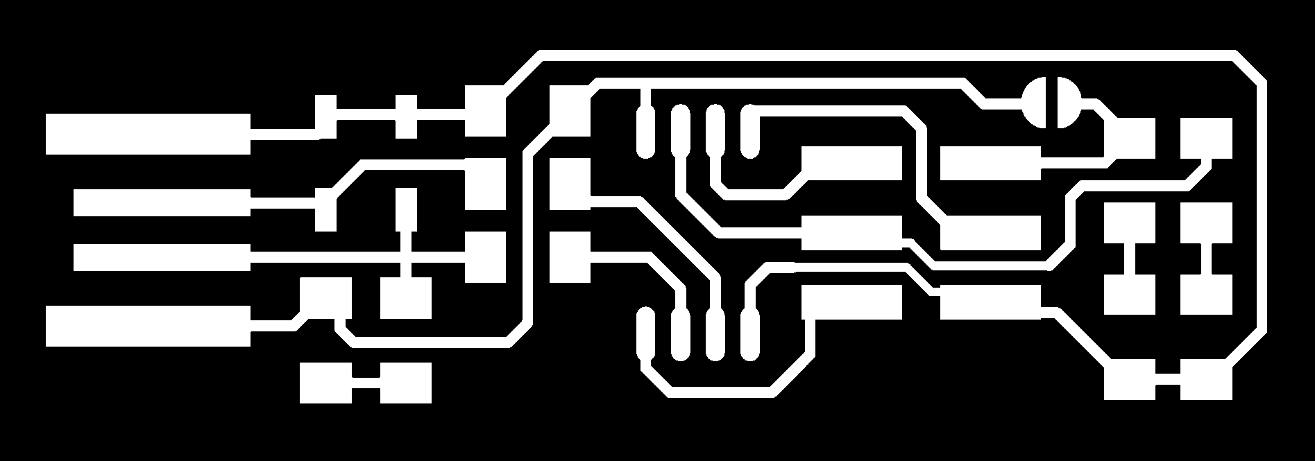
2. I downloaded the "traces png " file as well as "outline png" "FabTinyISP labeled board diagram" files the class site. The resolution is indicated, at 1000dpi.

3. I downloaded an PCB design software called "Autodesk EAGLE 9.3.1" educational version for Windows (64bit) from Autodesk Education Community website. Eagle is free for educational use and is valid for 3 years. EAGLE require an Autodesk ID to login.
Note :
- The default installation path of EAGLE "C:\EAGLE 9.3.1"
- Storage space require : around 530MB
- Default storage of EAGLE project files : "C:\Users\{UserName}\documents\eagle\projects" folder
4. Launch Autodesk EAGLE, at the Eagle Control Panel, create a new project called "FabTinyISP" and create a new board.
5. As EAGLE doesn't import PNG file directly, it only import BMP file. Therefore need to use Microsoft Paint and convert to "Monochrome Bitmap" files, as the images black-and-white only. A two-tone color BMP file is easier to be imported into EAGLE.
Note : If the images is not in "horizontal orientation", I will rotate the image to be horizontal so that I can place the PCB material horizontally into the cut-out slot on the sacrificial board of the PCB (CNC) milling machine in the Fab Lab.

6. Import the bitmap file

7. Since white-colour being the traces as seen in the PNG/BMP file, so select white-colour to be imported and converted by EAGLE to traces/lines

8. Select "inch" as the unit and set the "Dots per inches" to 1000dpi as this resolution was provided in the class site. Click "OK" and run the import script. PS: If the resolution is not provided, you can get the reolution by using GIMP-> Image Property feature, or import the PNG file into mobs. Type "1" in the "choose start layer for 1st select colour" box and this will import the traces onto EAGLE "Layer 1 - Top" which is the (top etching) layer.


9. Visually check the FabTinyISP design and remove any unnecessay text/objects from the (eg. at bottom-left corner) of the design.

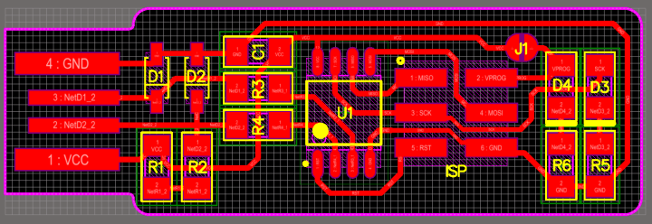
10. I imported the outline and added the text "Lucas" to my FabTinyISP board using EAGLE Text tool.
After placing the text object -> move mouse to point-of-origin (the cross) of Text Object -> Right-mouse-click -> Properties -> change the font size to the size you want -> check thet the font type is "Vector" instead of "Proportional Font" for engraving of the text.

11. [Optional] Run a DRC (Design Rules Check) to make sure my text entry is ok, before sending for milling. Following is my personalised FabISP board design in Eagle.
12. Save the board deisgn. The default path for EAGLE is "{username}\Documents\eagle\projects\"
13. Repeat the same steps shown above to create a new board design for the FabTinyISP outline.
Import the "outline" design (dpi setting of is 1000dpi) using default setting this time, EAGLE will import to the default layer which is "200" for BMP import.
14. Switch to EAGLE "Layer 16-Milling" and use the line tool to draw the outline for the FabTinyISP using a line width of 0.8mm as will be using a larger end mill to cut through the PCB material. Use the "Milter" EAGLE Editor command to create the curve corners.


Tip : if the outline is a rectangular shape like the "linetest" design, you can just draw/engrave the outline with the trace diagram, without creating a new board design for outline, and use a "hand shear" cutting tool to cut out the rectangular shape.
File :
My FabTinyISP board file in EAGLE :
myfabtinyisp trace brd
myfabtinyisp outline brd
15. I had downloaded the "pcb-gcode" plugin for EAGLE from https://github.com/febtop/pcb-gcode to convert my EAGLE board design into gcode. I extracted the files into a newly created folder called "ulps" inside EAGLE software folder Eg. "C:\EAGLE 9.3.1\ulps\pcb-gcode-3.6.2.4", instead of extracting to the ulps inside the default "Users\My Documents\eagle\ulps" folder.
Pcb-to-gcode is a User Language Program (ULP) for EAGLE produced by John T. Johnson Software LLC. Pcb-gcode ulp generates the required "gcode" file for "mechanically etching" the PCB board using any standard CNC milling machine (or router) to cut the traces out of the copper on the board. For more infor, please see "pcb-gcode-3.6.2.4/docs/pcbgcode.pdf". However take note that this plugin is a very old program and might have incompatibility issue with latest version of EAGLE.
16. Go to Eagle Control Panel -> Options -> Directories -> Set User Language Programs -> browse to the pcb-gcode folder and add in the path (like ";$EAGLEDIR\ulps\pcb-gcode-3.6.2.4") behind the default "$HOME\EAGLE\ulps" path. This is also stated in the documentation.

17. At EAGEL Broad Design -> Go to Main Menu -> File -> Select the pcb-gcode directory -> select "pcb-gcode-setup.ulp" and run the user add-in script

18. At the pcb-gcode ulp window, click the "Machine tab" to view the machine options and set the units to "millimeters", which is the standard measure format in Singapore. follow by adjusting the settings. Then I went to the first screen which is the “Generation tab“ and configure the setting. I selected “single pass“. When everything is ok, I clicked “Accepted and make my board“ to generate the gcode file for milling.
Some of the Machine Setting of pcb-gcode ulp:
Z High : 12.7mm (height to clear any obstructions like clamps or fixtures that hold the PCB down)
Z Up : 2.54mm (height for mill bit to raise and move from location to location)
Z Down : -0.15 (Depth into the board that the tool should cut when etching)
Drill Depth : -1.5 (Depth to drill/cut through the pcb board. (Thickness of my FR1 pcb board is 1.5mm thk)
Tool change : X-0, Y-0, Z-25.4mm (position to move to when the mill bit (tool) is to be replaced)
Tool Dia. : 0.1mm (diameter of the mill bit (tool) used to etch). PS : Actual tool dia might be larger like 0.4, but pcb-to-gcode program will produce error when setting other too dia other tahn 0.1mm
Feed rate : Etch : 20 (speed of etching x - y), 75 (for etching z axis)
Feed rate : Mil : 20 (speed of milling x - y), 75 (for milling z axis)
Generate top outlines - Generate g-code for top-etching, to cut out the tracks, pads, on the top side of the board.
Generate milling depth - Generate g-code for milling, how deep to cut through the board.
Single Pass : When turn on, the cutting tool will make only a single pass. Uncheck this option to configure the cutting tool to be able to make several passes around the tracks at an increasing distance each time, eg. used to cut throught pcb board.


19. Observe the pcb-gcode previewer window that pop, look out for any pads or traces that might be too close together forming an unwanted "bridge", lines that might be too thick that touches/crashes with each other, etc
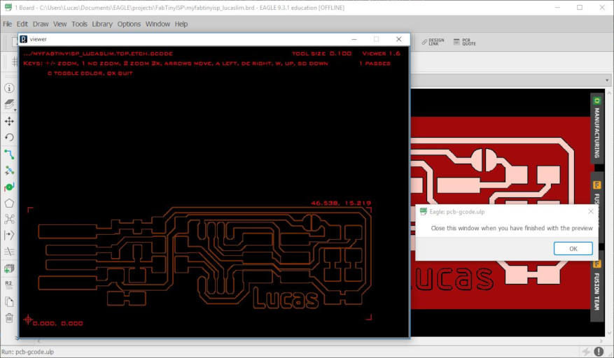
20. The gcode file is saved in the default C:\Users\{username}\Document\eagle\{myproject} folder (example "C:\Users\Lucas\Documents\eagle\projects\FabTinyISP"). Located the file "myfabtinyisp_lucaslim.top.etch.gcode"" and copied to a thumbdrive to be loaded on the PC connected to the STEPCRAFT CNC milling machine (router).
21. For "outline", in pcb-gcode, select "generate milling depth" and set to usually half the size of tool diameter used, so set "0.41". Manually modified the millling gcode file to have mulitple passes, using incremental increase of depth of 0.41 after each pass.

File :
My FabTinyISP gcode file :
myfabtinyisp traces gcode
myfabtinyisp outline gcode
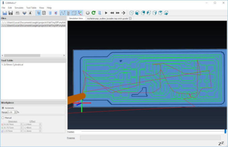
22. I have two gcode files, one for traces and one for outline. For the outline, it is running multiple passess and increases in the depth.
So I run a simulation of both traces gcode and outline gcode together using CAMotics to observe the cutting process. Notice for outline, the cutting tool run multuple passes and cuts very deep down.
23.
The Fab Lab @ T1442 has a “STEPCRAFT 420“ desktop PCB (CNC) milling machine (or also known as a router) to mil my pcb board and Mr Steven, my Fab Lab instructor, had taught me how to use the PCB milling machine.
STEPCTAFT 420 PCB (CNC) milling machine :

I am using 0.1mm V bit (v-shape engraving bit) at 10 degree angle.
The PCB material used is FR1 75x50mm single-sided Copper Clad Laminated (CCL), which is a thin layer of copper (for PCB engraving) over a non-conductive phenolic resin.
Mill Bit for traces : 0.1mm v-bit at 10 degree
Mill Bit for milling outline : 0.8mm end mill
PCB Material : FR1 75x50mm single-sided Copper Clad Laminated (CCL) PCB board. 1.5mm thickness.

24. Vacuum the sacrificial board (also known as spoilboard) on the Stepcraft machin to make sure it is free from dust.
25. I used a double-side tape to secure the pcb board to the sacrificial board.


26. Load the gcode file “fabisp.top.etch.tap“ into STEPCRAFT software

27. I calibrated the x and y-axis first. To speed up the movement of the milling bit into position, I set the "job feed %" rate at "40 %" and set the movement to "Continuous" mode. I will leave the calibration of the Z-axis to a later time, as I want to "air-print" my traces first.

28. I "air-printed" my design to check that the drill bit does not unexpectedly move out of intended milling area and hitting anything. This is done by adjusting the z-axis (height) to a height above the nearest obstruction, above the side metal rail
29. I calibrated the z-axis by using the Stepcraft Z zero accessory.

30. Start milling the traces for the FabTinyISP board


31. Milling the outline for the FabTinyISP board


32. After finsihed milling, used a very fine grade sandpaper to lightly brush the surface and sides of the milled board.
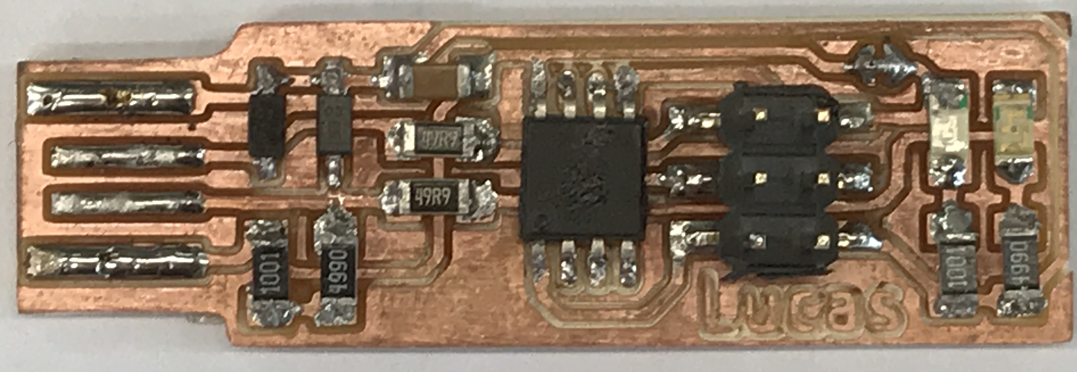
33. My milled FabTinyISP.

34. I tested the traces on the PCB by using a Digital Multimeter. Testing on any problematic circuit path. This is an very important step as this allow you to check for any problem and avoid costly mistake later on. I set the multimeter setting to "ohm" and enable the multimeter to provide an audiable sound when I doing the testing.
Soldering simply means the generating of heat using an electrical source to melt a metal (solder wire) to join two things together to form a connection.
Soldering is one of the most fundamental and handy skills in the world of electronics. Being new to soldering, I took around one day to practise my soldering skill using the soldering training kit provided by my instructors. I also made a few mistake in soldering my actual FabISP baord and "shorted" the circuit. It took me about two tries to get it right.
Soldering station : HAKKO FX-950 soldering iron, with adjustable temperature (made in Japan)
Solder (material) used for "stuffing" : 0.15" (0.3mm) Dia, 63% tin, 37% lead, 1.2% Flux, solder wire
Solder (material) used for usb connector : 0.028" (0.71mm) Dia, 60% tin, 40% lead, 2.2% Flux, solder wire
Soldering Safety : Soldering in an well ventilated environment. Wearing of safety glass
Soldering temperature : 275 to 300 degree celcius (need to test your soldering iron as temperature reading on soldering station might not be accurate)
My instructor passed to me a soldering practicing kit to start practising the soldering of various type of SMDs (surface-mount devices) components; starting practising on the "1206" components, then to "0805", then to "0603" and the rest. "1206" refer to their package/size being 0.12 inch x 0.06 inch.


The components are also known to as SMDs (surface-mount devices), which typically refer to the components that need to be solder directly on the surface of the PCB. The SMDs "package" is "1206". "1206" refer to their size being 0.12 inch x 0.06 inch, which is a much bigger size.
Components for my FabTinyISP in "1206" package :
1x ATtiny45
2x 1kΩ resistors
2x 499Ω resistors
2x 49Ω resistors
2x 3.3v zener diodes
1x red LED
1x green LED
1x 100nF capacitor
1x 2x3 pin header

Components for ISP 6-pin cable :

35. My learning journey on soldering SMDs :
- soldering environment : brightly lit work table, well ventilated work desk
- solder wire : for soldering SMDs, I used a thinner 0.4mm / 0.5mm solder wire. Leaded with flux core (rosin core).
- Soldering temperature : around 250 to 300 degree, but test the soldering iron tip is up to a temperature by briefly placing the solder wire on the tip to see if it melt, the solder should melt instantly
- Soldering timing :
- Apply tip on copper pad and the leg of the component to heat them up a bit. Count "one thousand", "two thousand". Then feed the solder to the joint, count "three thousand","four thousand", then remove the iron.
- Be quick to solder, as prolong and excessive heat might damage the componenets
- Use the side of the soldering iron tip (and not the point end of the iron tip)to touch the copper pad on the PCB and the leg of the component to heat them up a bit. Position the tip in a manner to have maximum surface contact between the tip and the pad and leg. Then feed the solder wire over it. The solder wire should easily melt and flow down the leg onto the pad.
- Soldering amount : Less is better, try to use less solder for joints
- Which to solder first : I soldered the "ATtiny45" first. Then moved on to solder the ressitors, then the rest.
- De-soldering : I solder the LED diodes in the wrong orientation, by assuming the "T" marking on the LED diode represent the "cathode" and had to de-solder the LED diodes. De-soldering by using the tweezer to hold onto the componenet that you want to remove and lifting it up from the table. Then by browing a hot air gun at it's joints at say 300 degree celcius and after a while the FabTinyISP will drop onto the table.
- Steps :
1. Rest both both my elbows on table rather than raise my arms in the air during soldering, this prevent both my arms from getting tired easily.
2. Prep the pab of the PCB :
- Apply flux to wet the pad to prep the surface. Flux is a chemical mixture that prevent oxidation and help to sort-of clean the copper surface.
3. Prep the soldering iron tip :
- Checking tip before solder, it should be silver in colour or shinny. A dirty tip is hard to solder.
- Before soldering we need to prep the tip which is also call "tining" the tip. "Tining" the soldering iron tip is melting a bit of solder on ironing tip. When you put a metal over about metal is call "tining". This light layer of solder helps prevent oxidation on the tip and helps the solder to flow more easily. After tining, clean the tip by brushing the tip on a brass sponge or solder sponge. The tip will look shinny. After tinning, immediate start to solder. Cleaning is by putting solder on the tip and cleaning it with a metal sponge.
Re-tin and clean the tip peridoically.

Note :
Resistors :
As there are a couple of different resistors, I need to check for the correct code of the resistors to be use.
Resistors Value :
R1, R6 : 1 K ohm (Code :1001)
R2, R5 : 499 ohm (Code :4990)
R3, R4 : 49 ohm (Code :49R9)
Diodes (zener diodes as well as the LED diodes) :
The diode has two terminals (or pins) and these terminals are "polarized". The positive end of a diode is called the "anode" and the negative end is called the "cathode".
On Brian's schematic diagram, the "cathode" is represented by the "vertical line" on the LED diode symbol and is facing toward the resistor and in-turn leading to the "GRN". On the physical diode, there is a very tiny and sometimes hard to see line at the terminal that represent that this pin is the cathode. To double check you can use a digial multimeter and set to diode mode and use the black-color (negative) test probe and red (positive) test probe of a digital multimeter to check the polarity at the ends on the diode. The voltage will only flow in one direction through the diode.

Jumper :
J1 form a temporary connection of the two contact pads together.
Soldering components :
Placing a tiny drop of solder on the pad. Then with one hand using a twister to place the componenet and with the other hand holding the soldering iron to melt the solder on the pad. This secure the componenet in position while you solder the other end.


36. Use a "paint pen" and do a marking on the 6-pin to indicate pin 1.

37. My finished FabTinyISP is a bit thin and hang loose when inserted into the usb port, so I had cut to shape of the FabTinyISP and pasted underneath the FabTinyISP.
Put one end of the ribbon into a 6-pin terminal header and use a clamp to clamp the ribbon and terminal tightly together. Then do a marking to indicate Pin 1 at both the 6-pin terminal ends


1. Do a visual inspection of the board to identify any problem, cold solder joints, missing componenets, componenets mounted in wrong orientation, etc. "Re-work" if necessary.
2. Then use a digital multimeter to test the path to see if there is no short circuit. Checking the VCC or GND paths with its components along these path. "Re-work" if necessary.

A short write-out on the usage of a digital multimeter is availabe in my Week 7 - Electronic Design week.
We are using either the AVR microcontroller (or call AVR chip) known as the ATTiny44A or the ATTiny45 in class.
Before we start to program the AVR microcontroller, we need to obtain/install a couple of software tools, firmware and/or libraries. These software tools are seperate, stand-alone software and not integrated together as one. These are refer to as "toolchain" for programming the AVR microcontroller.
The "Toolchain" therefore refer to a set (or collection) of tools/libraries from writing program to the programming of the AVR microcontroller. This includes compiler, assembler, linker and Standard C and math libraries.
Toolchain basic overview :
1. [Writting Code] Write your source code (eg. in c programming language) with a simple text editor
2. [Compile] Compile your source code into machine code with a open-source compiler. Machine code refer to the .hex file generated.
(the compiler I am using is "avr-gcc")
(at command prompt, type "avr-gcc --help" for more info)
3. [Flash Programming] Using an uploader software (avrdude) to send the machine code to the target AVR chip which store the instructions in its non-volatile flash memory. This process also known as "Flash Programming" since we are transfering code to the flash memory on the AVR Chip.
(The AVR chip only run on .hex file which is the machine code)
(PS : at command prompt, type :avrdude -h" for more info)
(AVR chip flash memory is like the BIOS in a Computer)
4. After the machine code has been written to the flash memory of the AVR chip , the AVR chip will automatically restart and start running the code
1. I followed Brian's tutorial on the class site to learn how to programm my FabISP. As I am still very new to Linux, so I choose to use the toolchain installation for Windows.
2. Download WinAVR from SourceForge website at https://sourceforge.net/projects/winavr/. WinAVR will be installed to "C:\WinAVR-20100110"
Note : Refer to "WinAVR-user-manual.html" located in the WinAVR-20100110 folder for more info on WinAVR.
3. During installation, WinAVR will automatically add itself to the "environment variable or system path" for the operating system to easily locate the avrdude executable programs.
4. Open the "Command Prompt(Windows)" and type "avrdude" and you will be able to see it is still an older version of "avrdude (version 5.10)". I downloaded the latest avrdude version 6.3 from http://savannah.nongnu.org/projects/avrdude and extracted to my C:\ drive.
5. Edit the system path and have avrdude ver 6.3 path moved above "WinAVR". Type "avrdude" in Command Prompt again and now it will show version 6.3.

6. Download and install the "AVR programmer and SPI interface driver for Windows" from https://learn.adafruit.com/usbtinyisp/drivers.
7. I connected my FabTinyISP to another (working) FabISP borrowed from my Fab Lab instructor. Refer to Brian's board design, ensure the cable ribbon is correctly connected, eg. connect pin-1 of FabISP to the pin-1 of FabTinyISP. Then I connect to my notebook. The Windows OS will detect the usb FabISP programmer and list the device in the "Device Manager" screen in Windows Control Panel.

8. To make sure both avrdude and my FabISP are connected correctly and able to talk to each other. I typed in "avrdude -c usbtiny -p t45" to check.
avrdude -c usbtiny -p t45
Syntax : avrdude -c {programmer : eg. usbtiny} -p {AVR chip on target board : eg. t44}

You can ran the command the following command to display a list of supported programmers/AVR chips by avrdude.
avrdude -c ?
//display list of programmers
avrdude -p ?
//display list of AVR chips
9. Downlaod the FabISP firmware (firmware_45.zip) from class site. Extract the zip file to a folder, example "C:\FabTinyISP Firmware".
10. Go to the folder that contain the firmware (C:\FabTinyISP Firmware\) and open the "makefile" to have a look. At the top, there is a brief introduction to the various make commands. In simple explanation, a makefile is used to simplified running of various seperate tasks(or instructions), it is like one single file that contains all the common tasks (or instructions) that you can run.

11. I ran the command "make" to compile the source code (which are written in C) and finally generate the .hex file. Notice here is the use of "avr-gcc"

12. I ran the command "make flash" to flash the target chip (FabTinyISP). Notice here is the use of "avrdude to transfer the hex file to the target board".

13. I ran the command "make fuses" to programs the fuse bits on the target chip (FabTinyISP)

14. I ran the command "make rstdisbl" to blows the reset fuse on the target chip (FabTinyISP).

15. To make sure that I had programmed my FabISP. I unplugged the other FabISP Programmer and plugged my FabTinyISP to my notebook. From Windows "Device Manager", I saw that my FabTinyISP was recognized by my computer.


16. Testing my FabTinyISP by connecting to another FabISP (Note: the targetted FabISP must be in programmable mode which mean that it's jumper should not be dis-jointed) and plugging my FabTinyISP onto the usb port of my notebook. Then run the command "avrdude -c usbtiny -p t44". The result show that my FabTinyISP is ready!


17. Disconnect "J1" by removing the solder. This will prevent accidental writting to the FabTinyISP in the future.

Being totally new to the world of electronics, I find this week lesson and assignment to be overwhelming and tough. Thankfully, my Fab Lab instructors, Mr Steven and Mr Rodney, were very patient and kind to teach me and guide me along.
The hardest part for me was soldering all those tiny SMDs onto the surface of the PCB. It took me about 3 to 4 days to learn the soldering technique and improve my soldering skill. I had learn the importance of applying a bit of the flux (or soldering paste) on the pad helps a lot in the soldering process. Another is to constantly re-tin and clean the tip peridoically with a metal wire mesh tip cleaner or sponge.
Learning about all those parameters to set for the etching process also took me some time to learn.
I had cut my finger against the sharp tip of the 0.1mm v-bit (10 degree) twice. Once while changing the v-bit on the Stepcraft machine, the other time was while removing the v-bit from tit's box, by placing my finger on the tip/top of the plastic cover and taking it (the v-bit) out of the box.

Always hold the v-bit by the sides while removing the v-bit from the box, and do not touch the tip/top of the plastic cover
After completion of the making of my FabTinyISP, there is a great sense of joy and sastifaction. I realised I had grown in exprience and is now more confident in soldering too.
My FabTinyISP board file in EAGLE :
myfabtinyisp trace brd
myfabtinyisp outline brd
My FabTinyISP gcode file :
myfabtinyisp traces gcode
myfabtinyisp outline gcode
Wikipedia : In-system programming
Wikipedia : AVR microcontrollers
ATtiny24A/44A (AVR microcontroller) Datasheet - MIT Fab Lab
Wikipedia : Atmel AVR ATtiny comparison chart