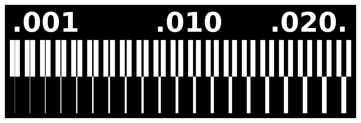
To check the precision, limitation and design rules for the PCB production process I used these sample pattern:
LineTest
Outline of the test pattern

By using Fabmodules I converted the sample pattern from .png to .rml since the milling machine can only take .rml input.
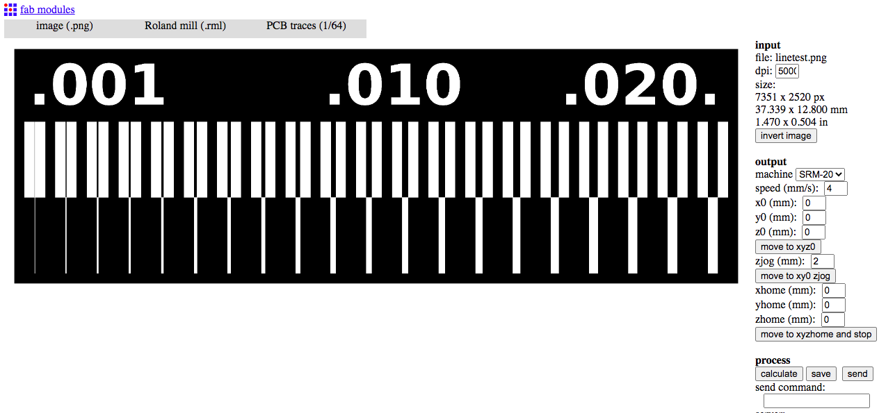
Generating the PCB traces and saving the .rml file:
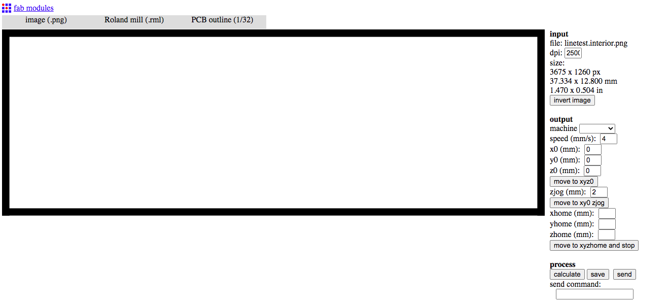
Importing the outline in Fabmodules:
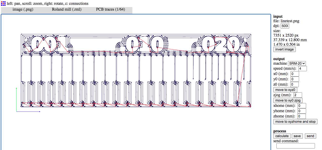
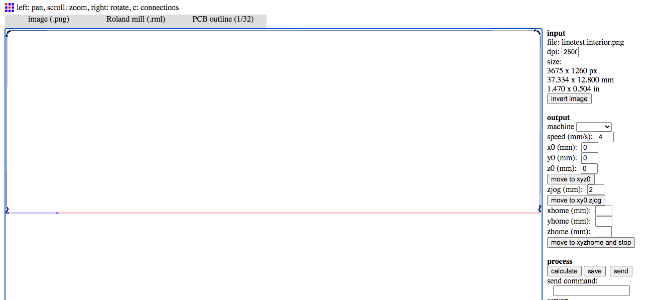
Generating it's path and .rml file:
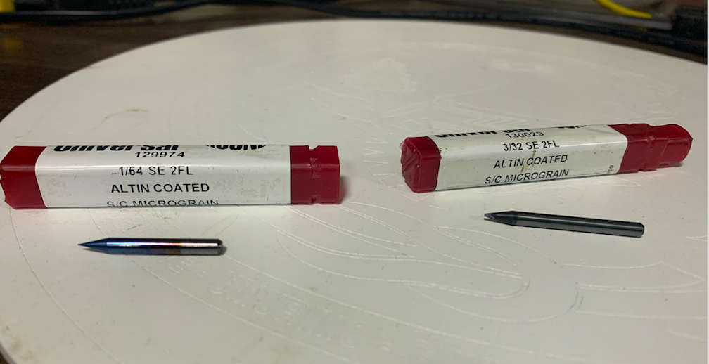
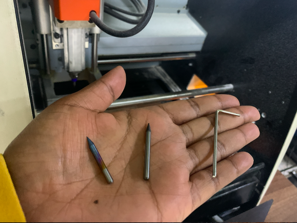
Here is the two types of tools to be used in milling the pattern (1/64) and outline (1/32)
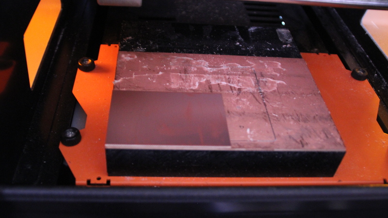
Setting the PCB plate and polishing the surface:
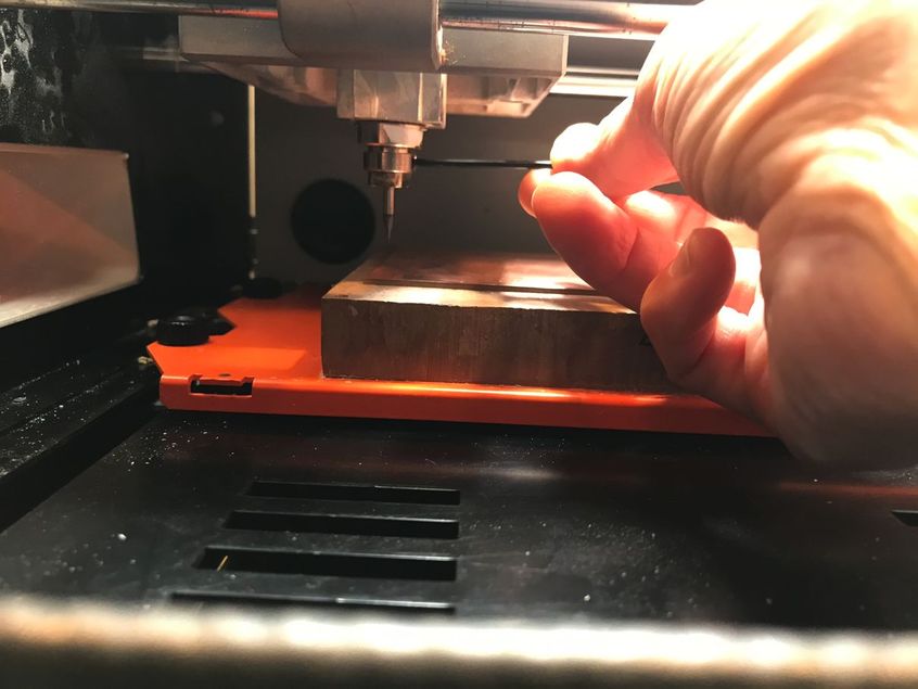
Setting the zero point of the z-axis:
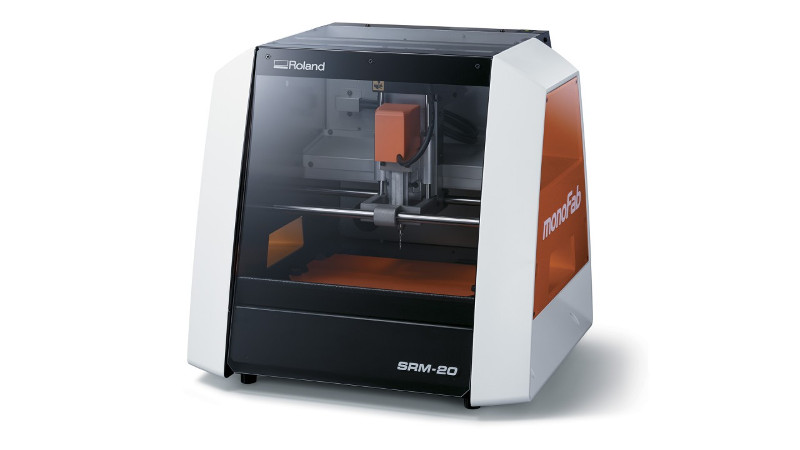
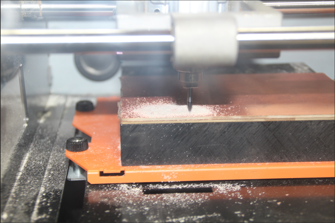
Milling the pattern and outline
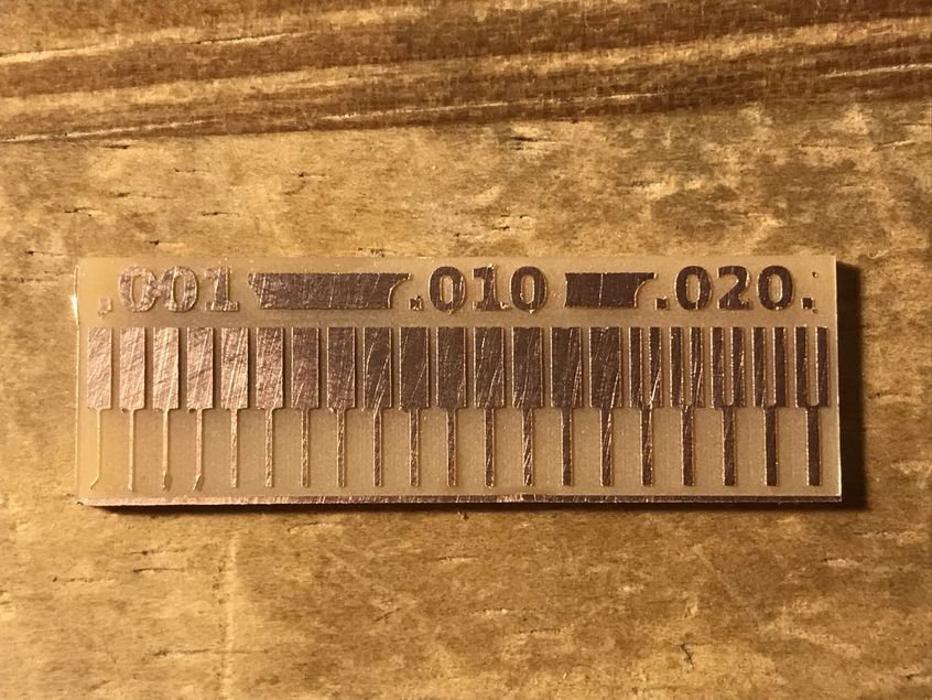
The tool diameter is 1/64 = 0.0156 inch which is approx 0.016 inch. For the groove, 0.016 inch is located at fifth right and this seems to be the limit. For the trace width, 0.005 inch looks like the safety zone, referring on the fith left trace.
I first downloaded the png files for traces and board outline here:
Traces (1000 dpi)
Outline Cutout (1000 dpi)
These are the FabISP images for traces and board outline I used for milling the PCB
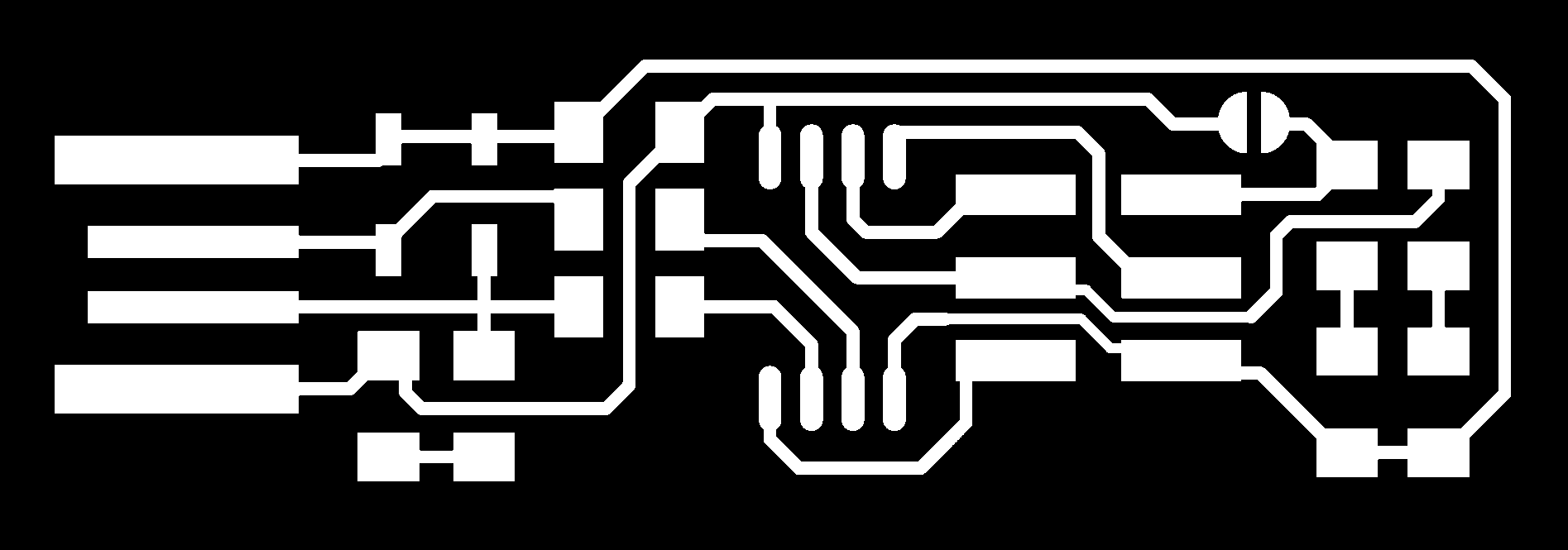

First we need to import the image into Fabmodules to generate the .rml file for the milling machne. After importing the image into Fabmodules, we need to select the type of our machine and set the axes to origin.
After clicking on calculate, it generates the path:
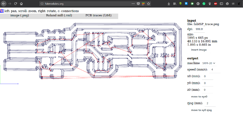
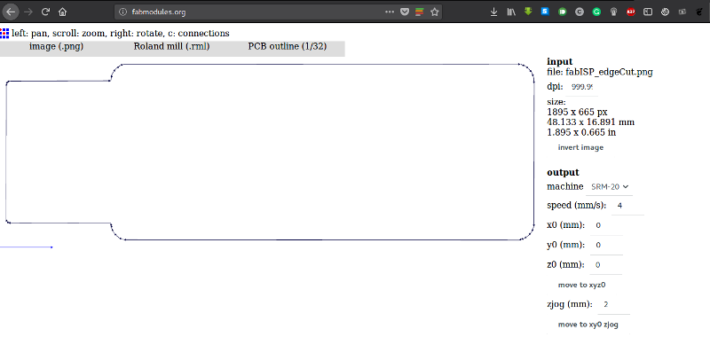
I also imported the board outline to generate its path :
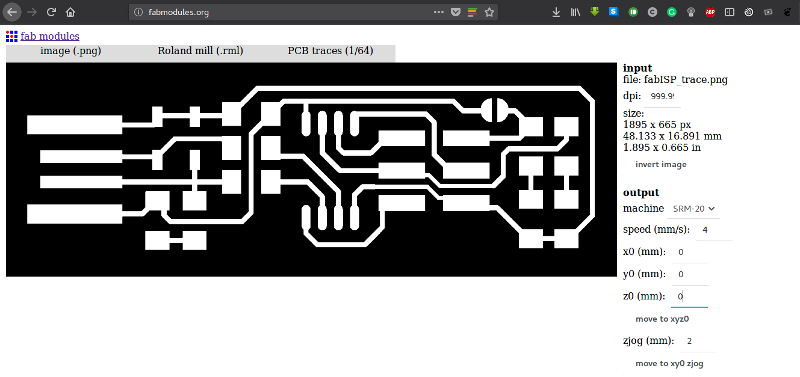
Here iis the .rml path file for the machine:
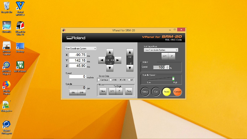
After downloading the .rml file, we have to import it in the VPanel for SRM-20 software in order to trace it. Here I had to first set the XYZ axes positions:
Next, I tapped the FR4 board :
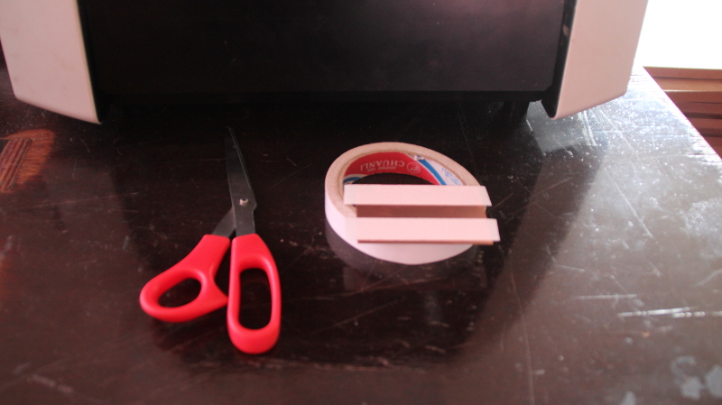
Next, I fixed it to the sacrificial board that is fixed on the machine bed:

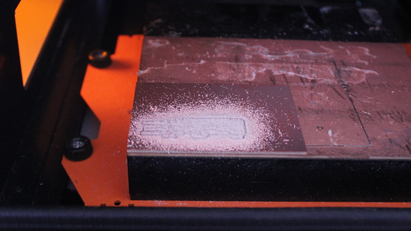
Milling the PCB: one tool broke while I was printing and I had to replace it. This was due to the fact that I didn't level the PCB board properly. After, I had to always make sure that the tool is not forced into the board to avoid the breakage.
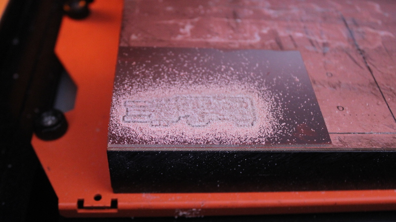
RESULT:
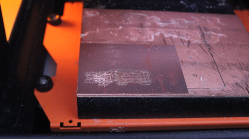
Tracing the PCB outline :
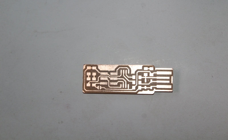
Final PCB result :
| No | Component | Pieces |
|---|---|---|
| 1 | ATtiny45 | 1 |
| 2 | 1K ohm resistor | 2 |
| 3 | 499 ohm resistor | 2 |
| 4 | 49 ohm resistor | 2 |
| 5 | 3.3 zener diode | 2 |
| 6 | Red LED | 1 |
| 7 | Green LED | 1 |
| 8 | 100nF capacitor | 1 |
| 9 | 2x3 pin header | 1 |
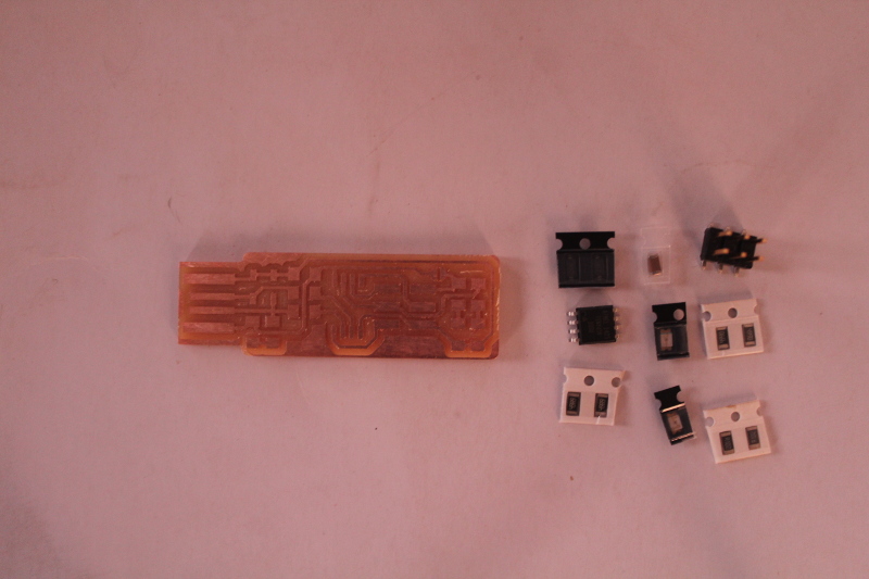
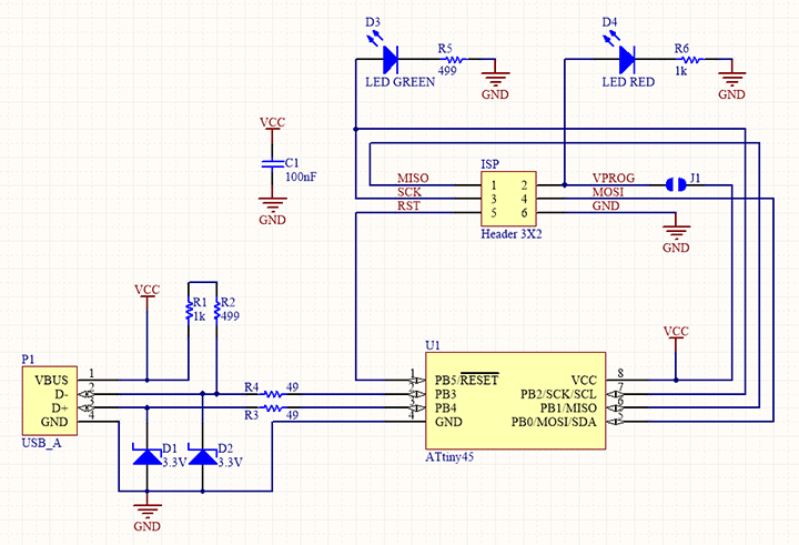
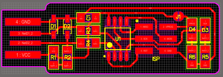
To solder the parts to the PCB I reffered to below schematic and board images for proper placement. I started the difficult part; soldering the ATtiny45 and the ISP header.
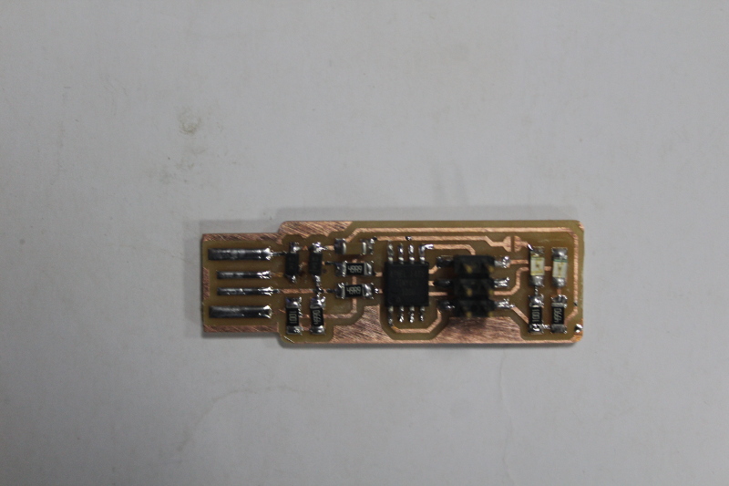
Here is the final result after soldering:
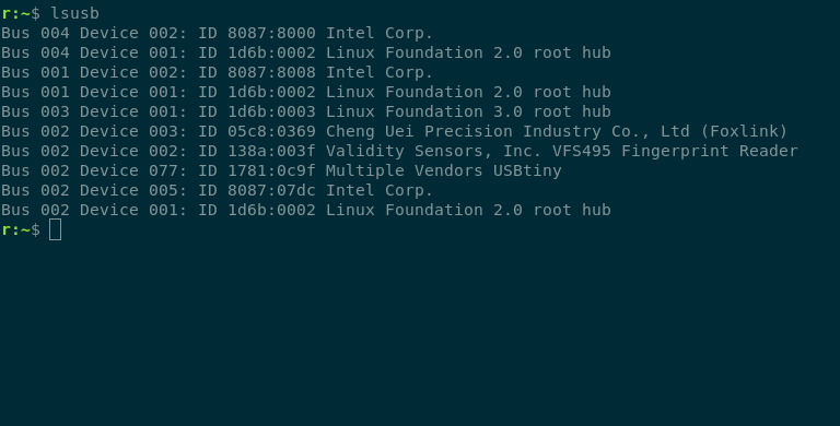
To program the board you have to connect the USBISP programmer in the computer and first of all try to see if the computer reads it.
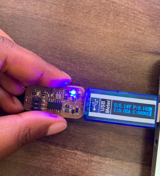
The computer recognizing the FabISP as USBtiny. Shown in the image below:
After I downloaded the firmware to be loaded in the programmer.Then run make flash in terminal to erase the target chip, and program its flash memory.
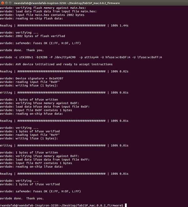
After above processes, a message appears saying that the Fuses are OK, meaning the USBtiny is ready as a programmer.
Files:
Download