We start the week with a basic explanation of electronics to have the necessary knowledge to design our circuit.
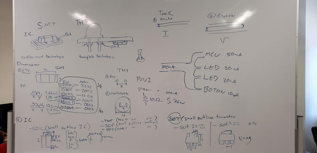
We learned the differences between the SMT (Surface Mount Technology) and the THT (Troughole Technology) components, which in our case, we will only use SMT.
For the tracks, to know the width and necessary space between components, if it is required to send to manufacture, it is possible to put very fine parameters, but in our case, when doing it by hand, it is preferable to put bigger measurements.
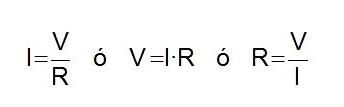
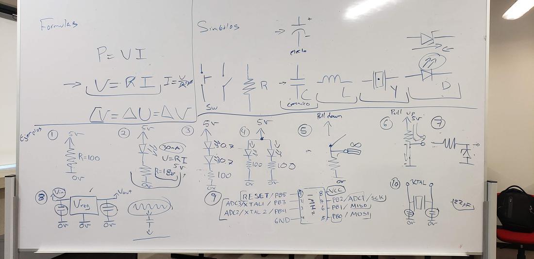
We learned about how to use Ohm's law that says that the intensity of current through a circuit is directly proportional to the voltage or voltage of it and inversely proportional to the resistance it presents. Its formula is:
Where I is the intensity that is measured in amperes (A), V the voltage that is measured in volts (V); and R the resistance that is measured in ohms (Ω).
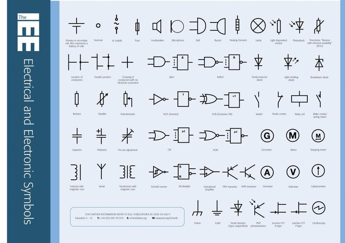
We learned about the basic symbology of electronics, an important point when designing circuits.
We learned about the basic symbology of electronics, an important point when designing circuits; as well as when it is a series or parallel circuit and a brief introduction to the Attiny 85 microcontroller.
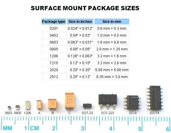
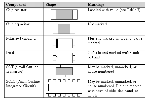
Another important point when designing circuits is the width of the tracks, the separations to be considered and packaging of the electronic components.
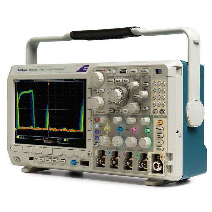
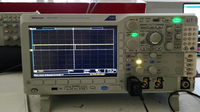
As a team, we went to the electronics lab where, with the help of an oscilloscope and a multimeter, we were able to measure a development card, in this case, an Arduino UNO.
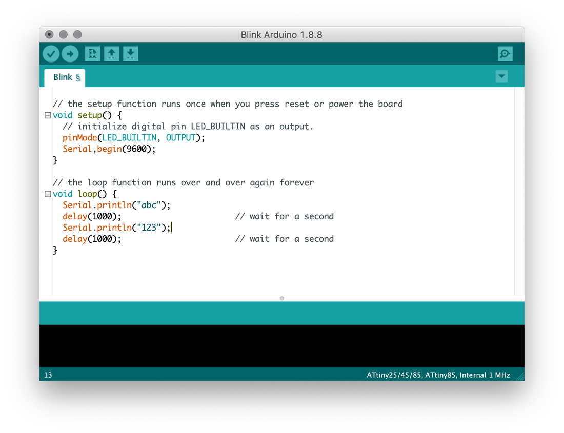
First we load a program to the card, we use the classic hello world of electronics, which is to turn on a led.
After loading the program in the arduino, with the help of an oscilloscope we proceeded to measure. We connect the oscilloscope tips and adjust the signal, then connect the tips to the card and measure the pulses that were sent when turning on a led.
It is a bit difficult to adjust the oscilloscope to capture and amplify the received signal and thus be able to visualize it better on the screen.
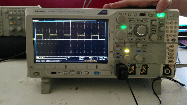
We loaded another program to the card, which sent 123 abc and we verified on the oscilloscope. With this we were able to verify signals from a PCB.
Being a digital signal the wave is square and not undulating as it would be in an analogous signal. If it is 0 the wave is down, if it is 5 the wave is high.
It should be mentioned that these are not totally real values, since there is a small range for each lower and upper limit.
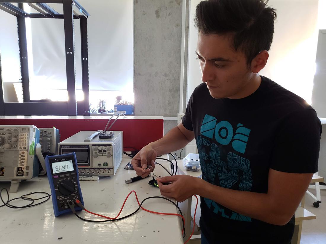
Then with the help of a multimeter, we measured the amperage, voltage and continuity, in this way we could use the multimeter to measure certain units of a PCB.
EAGLE //
EAGLE (acronym for Easily Applicable Graphical Layout Editor) is a program for designing diagrams and PCBs with a famous auto-router around the world of DiY electronic projects, because many versions of this program have a Freeware license and a large number of component libraries around the network.
To make a PCB design, we must first create the schematic, which is where the logic of the circuit goes, in it we will draw the representation of the circuit. It is necessary to add the components that are used and then connect them through cables.
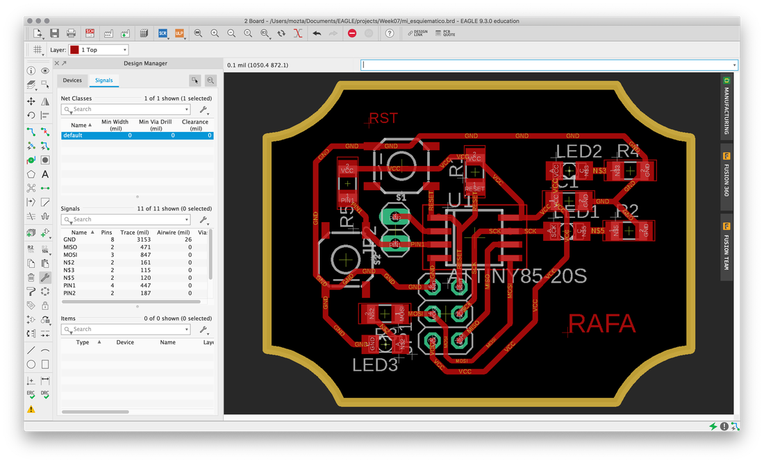
After creating the schematic the board is created, which is where the real connections of the components mediating paths will be.
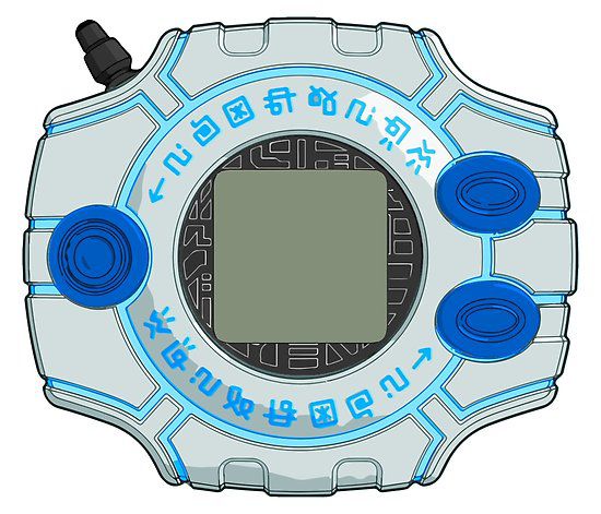
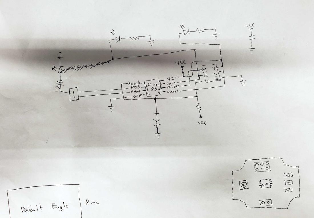
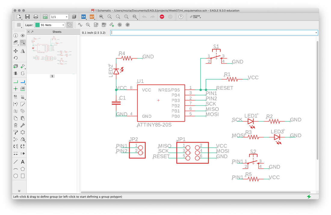
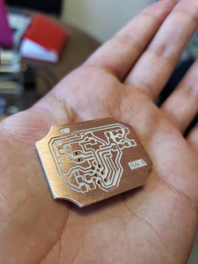
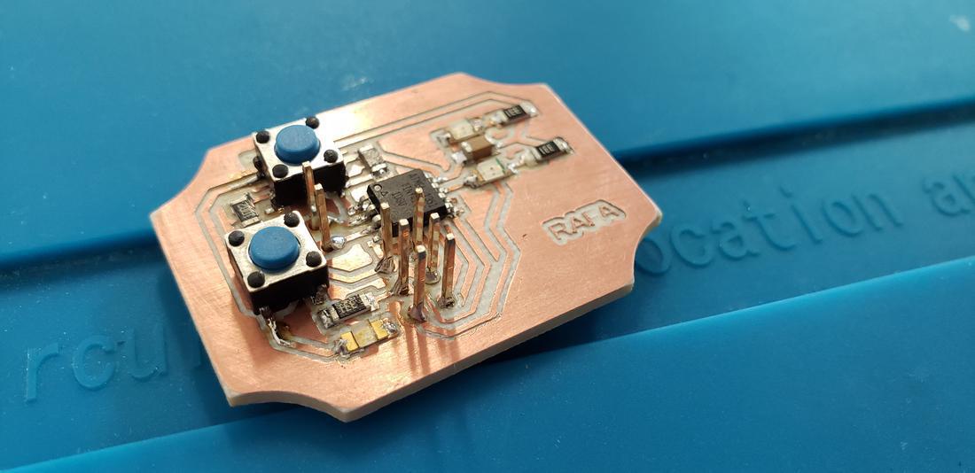
Before creating my PCB in Eagle, I decided to draw my circuit to have everything defined. I put an Attiny 85 as a microcontroller, some resistors, LEDs, buttons and a capacitor. Then draw the plate, for that I insipire in design of a digivice.
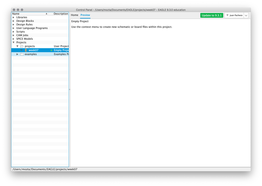
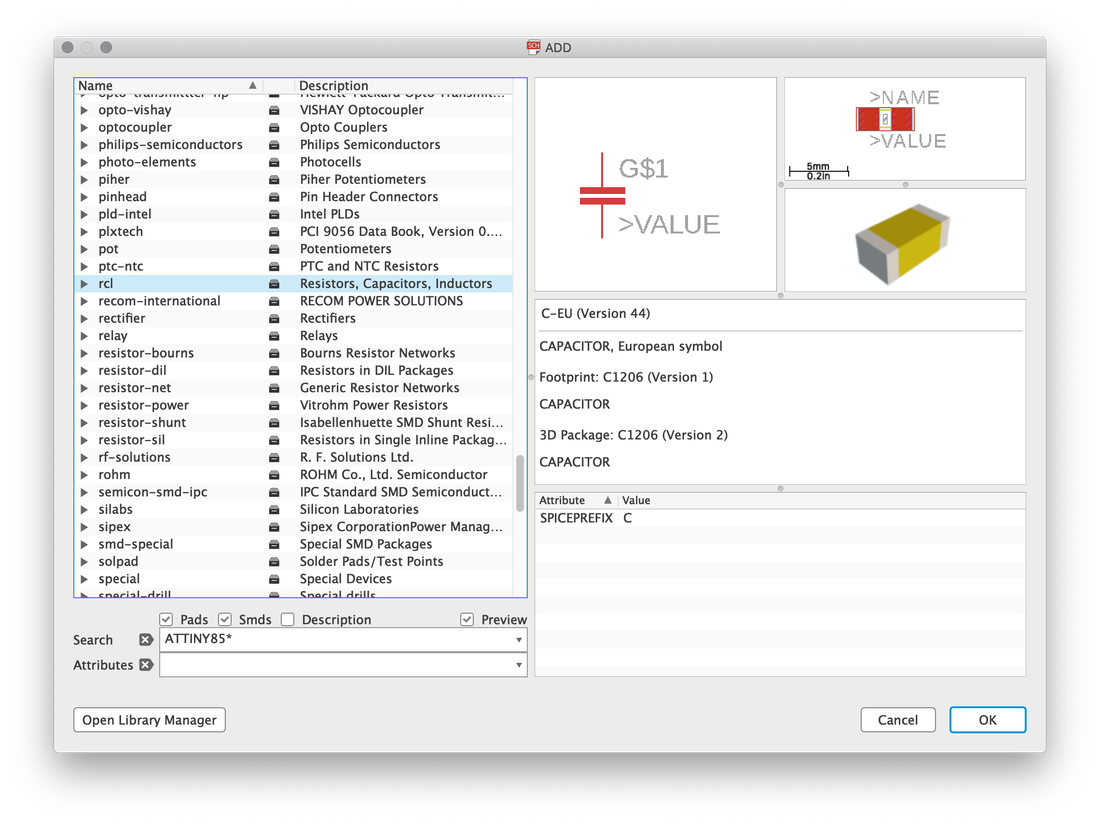
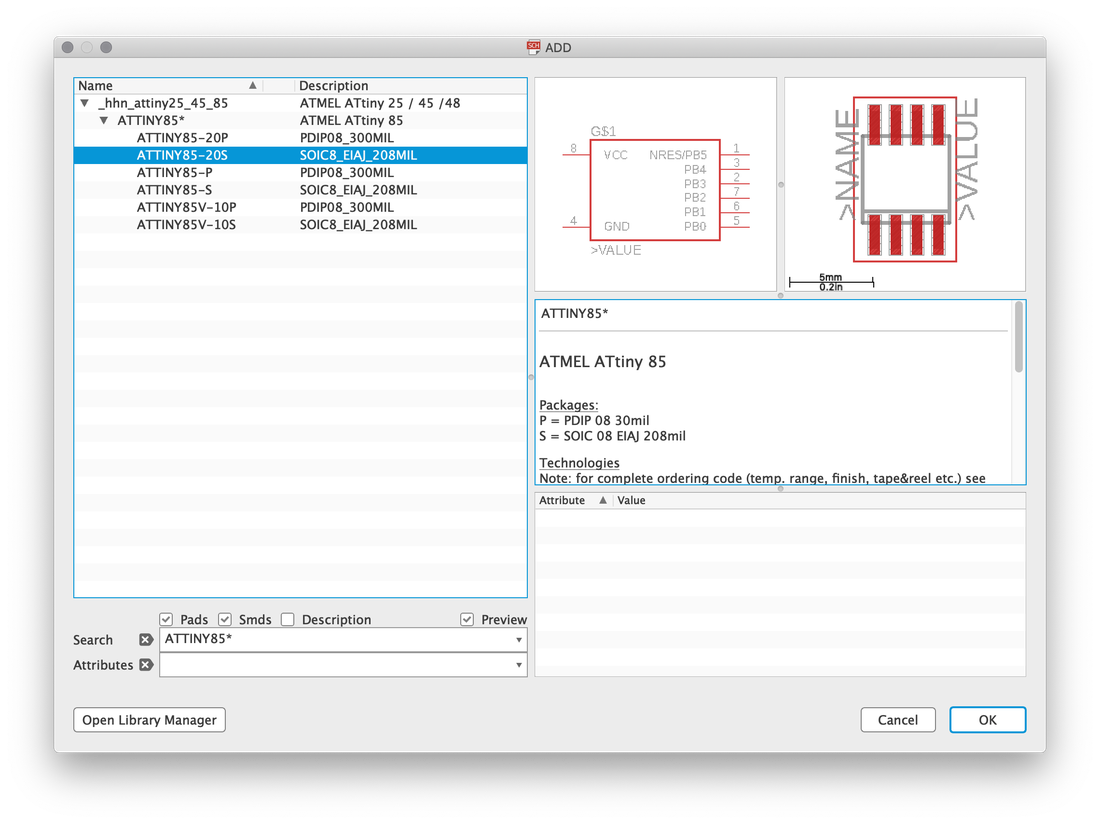
In EAGLE create a new project, where I added my schematic and started looking for the components I needed, however, in the first point, it was difficult to find the components I wanted, there were some that were not, so I had to look for them on the internet, download and install them, that is, put the new libraries in the EAGLE libraries folder, then from the control panel enable the new libraries to appear.
I did not find the Attiny85 microcontroller or the surface button, so I had to design them. I added all my components to the schematic window, saved and proceeded to connect the cables; making the drawing of my circuit on paper, I help a lot in this part, since I had it defined, it was just a matter of joining parts and ready. Save and I started to design the create board, the real interesting part.
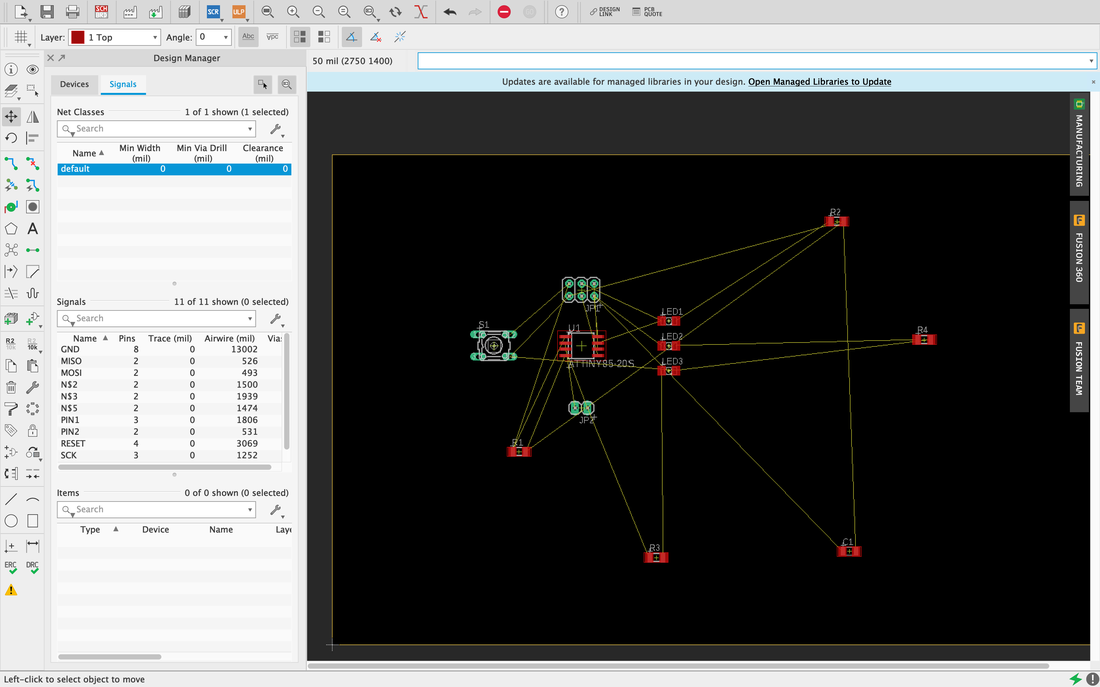
All the components appear below and outside the marked area, which is the area of the card, so you have to move them so they stay within the area. Afterwards and one of the worst headaches was to accommodate the components in such a way that when making the connections between them, they were all connected without getting in some wrong way or, cluttered tracks, tracks that can not join, closed roads since they stayed No exit, a great challenge.
After fighting for a long time trying to accommodate and connect everything in the best way, I managed to connect everything and without errors. The errors were something very notorious in this stage, since there were tracks to the air, overdraft tracks or tracks without exit.
Something that helped me a lot was to edit the design rules, where I modified the distance between tracks, pads and holes, as well as the size of the tracks. I also help to change the dimensions of the canvas, where adjusting to millimeters in 0.1 allowed me to move the components more freely.
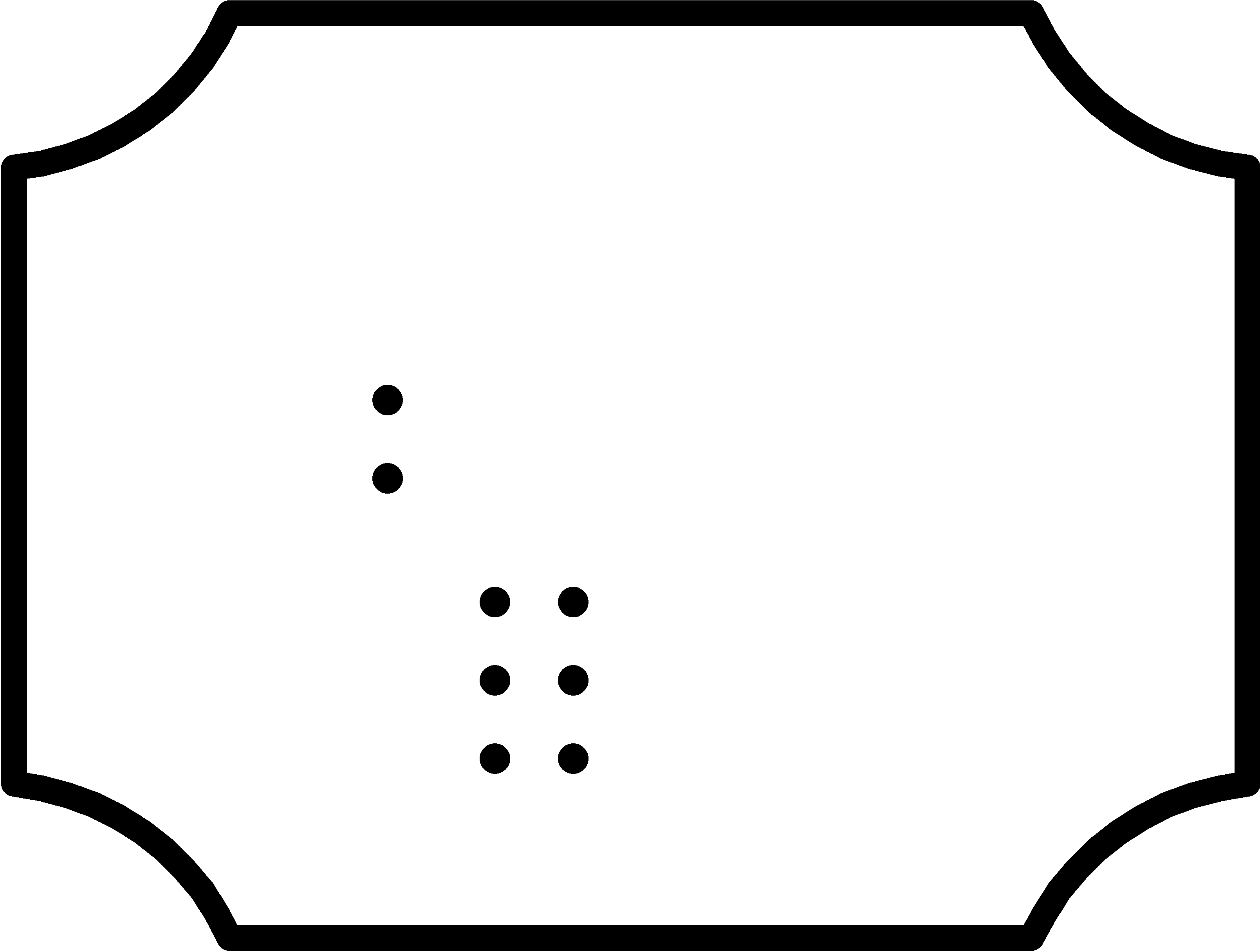
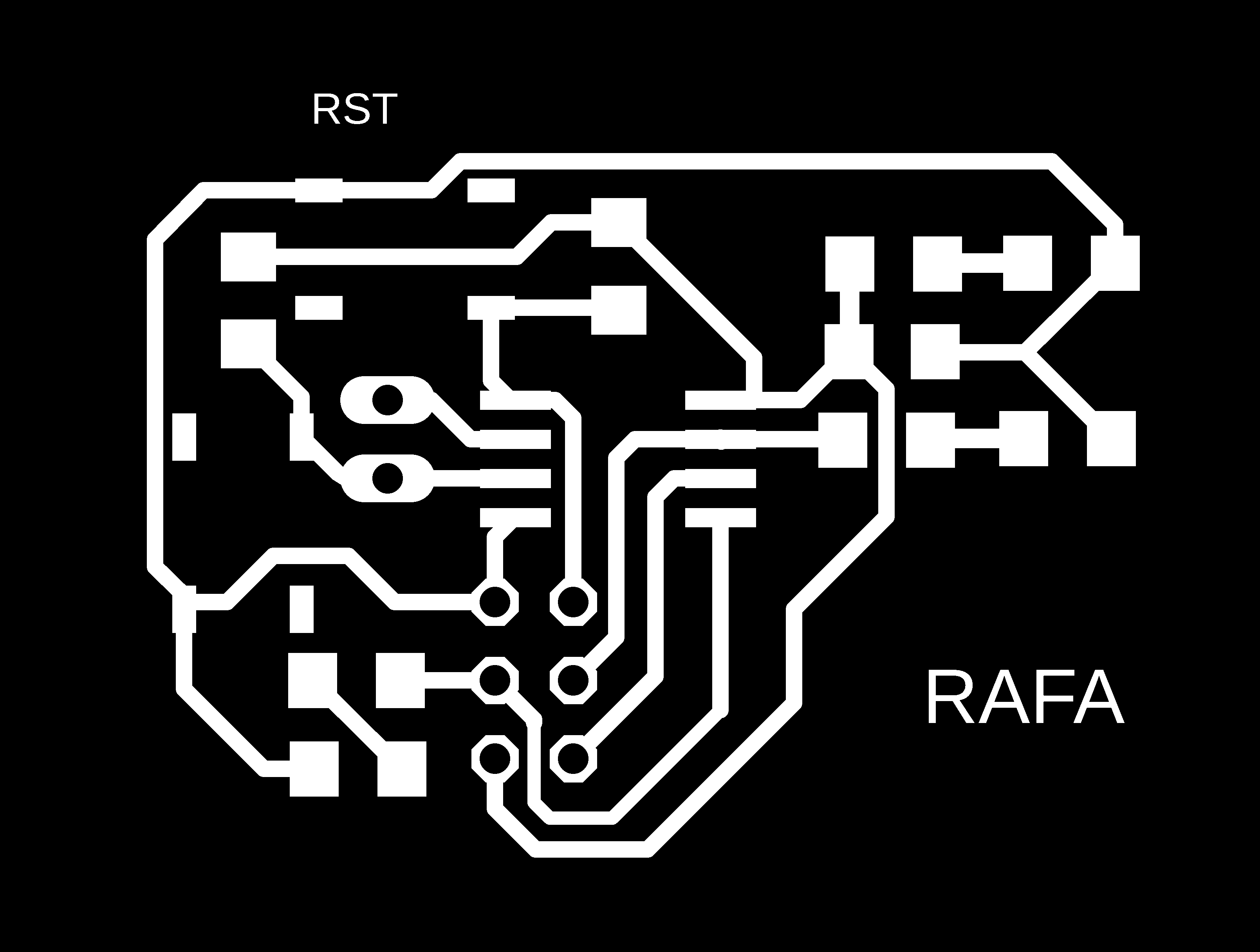
Once finished joining the components, I proceeded to draw the outline of my card, for it I had to delete the one that comes by default and with the help of the line tool forms a rectangle without joining the vertices, because here I join them with arcs, to give a more versatile appearance.
I also added some text, to start my name and then not to get confused, I added an "RST" tag where the reset button goes.
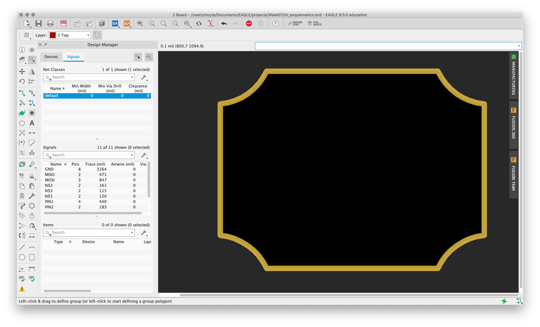
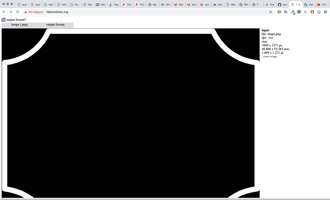
Modify the edges to 0.8 as they indicated to me and then in layers hide all the measurements except to be left with the contour, and export in PNG image with a resolution of 1000dpi and in monochromatic.
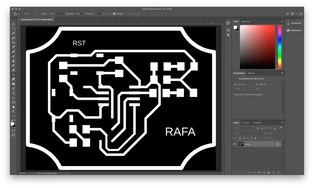
Next, hide the measurement layer and enable the Top, Traces and Tracks layer. In the same way export in PNG.
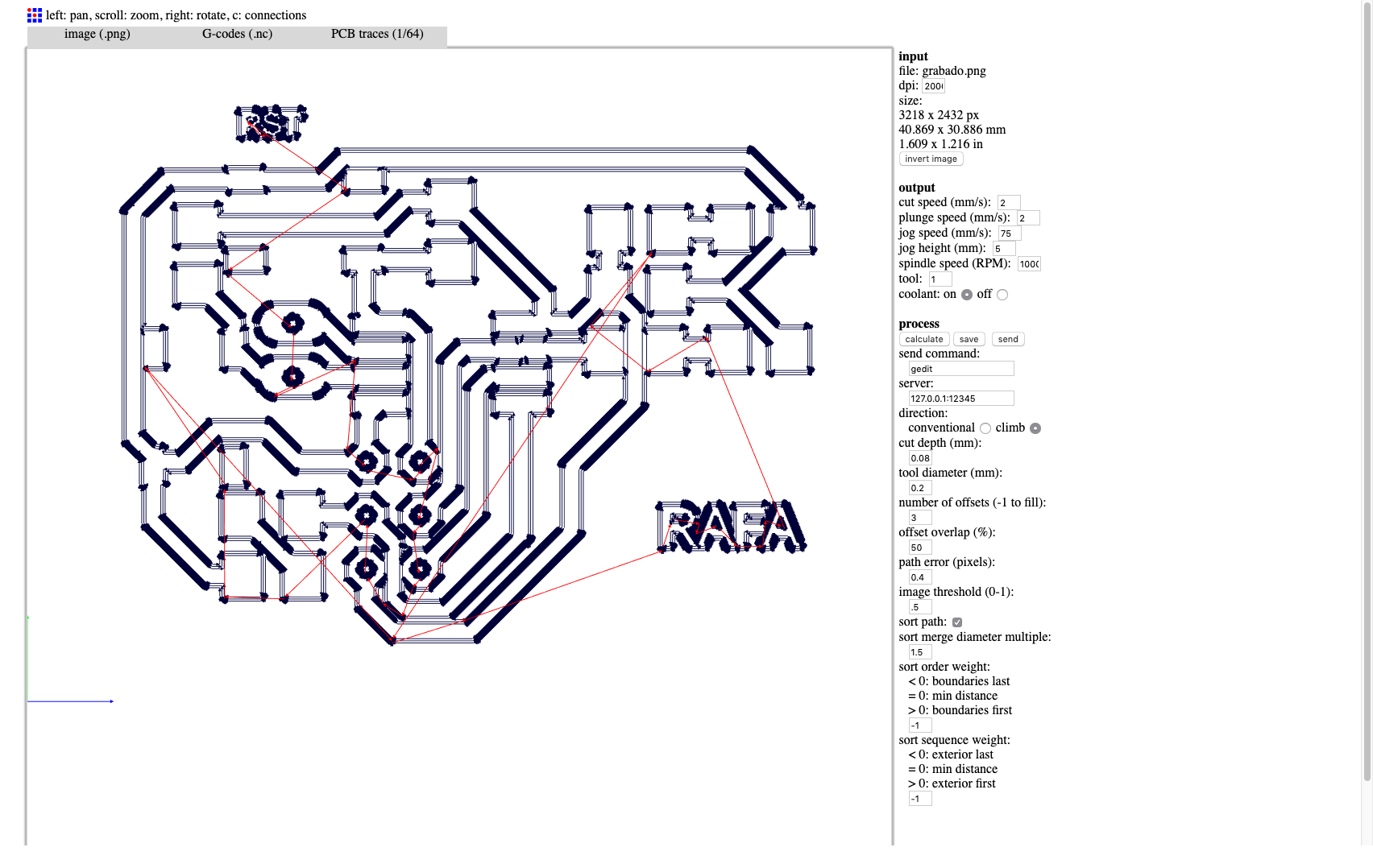
Then I went to the fabmodules.org application where I loaded my file to be able to convert it to RML for the model, but, for some strange reason, my design mediated more than twice as many dimensions, I was moving several parameters and nothing, until I opened it Photoshop and still measuring twice. In the end, I came to the conclusion that possibly in the Mac version, something strange was happening, so I got a Windows and Eagle computer installed, opened my files (schematic and board), I did the same steps to export in PNG and then load the resulting image into fabmodules and go! my circuit already had the real measurements.
Set the engraving values (1/32) of the model and export the result in RML format.
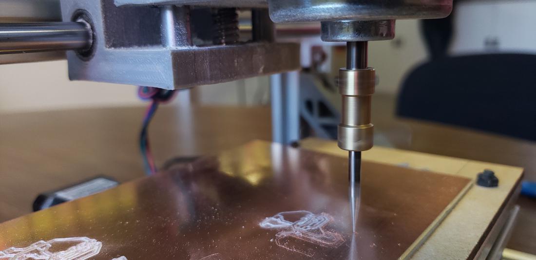
Then I opened the Roland software and loaded my file, put the engraving tip in the model, made some small adjustments and loaded my file and started recording.
First I did some tests before recording the actual design. I realized that I was recording too much, to the point that it seemed cut, instead of recorded. I spent a lot of time moving parameters until I could adjust it correctly and this was the result.
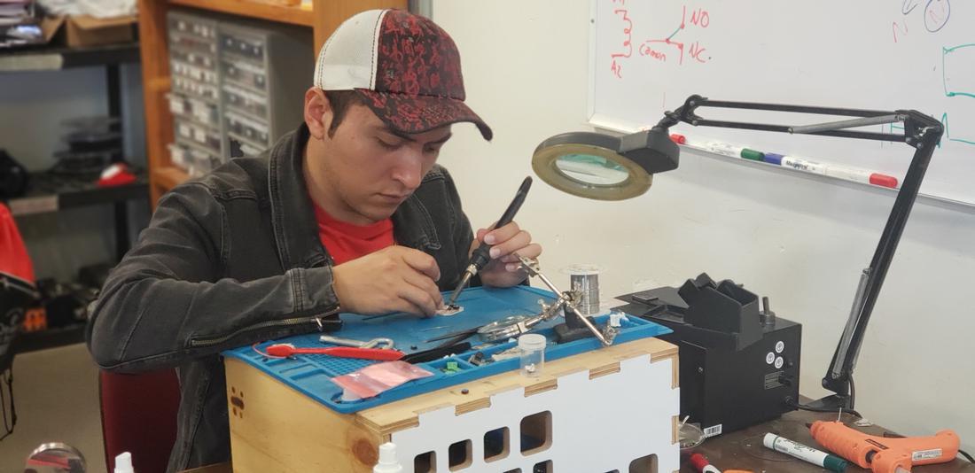
Finally weld the electronic components to the pcb.
And to verify that the PCB works, I will load a couple of programs.
The files //
Below you can find the download links of the original files created for this week.

 16.31.07.png)