Designing
Summary
Wired Network and Communications
- Design Node 0 Node 1 Node 2 Microcontroller Board
- Creat New Project & Sketch KICAD
- Import Fab Library
- Import Components
- Connect Components
- Give Compoents correct name and value
- Annotate the design
- Assign Footprint to Symbols
- Generate Netlist
- Open Pcb New
- Read in Generate netlist
- In Pcb New Set Design Rules (Setup -Design Rules)
- Rearrange Components and Make Traces
- Place your Auxillary Axis
- Plot Layers
- Flatcam
- Physical tool dia 0.40
- Cutz -0.1
- Travel Z 2.5
- Feed Rate 0.3
- Spindle speed 10000
- Passes 1
- Solder Node 0 Node 1 Node 2 Microcontroller Board
- Programming Node 0 Node 1 Node 2 Microcontroller Board
- Desigining version 1.0 Neal Design/ Flatcam
- Front Cut
- Cutz -0.15mm
- Travel Z 2.0
- Feed Rate 3.0
- Tool Dia 3.0
- Spindle Speed 10000
- Passes 1
- Pass overlap 0.17
- Edge Cut
- Tool dia 0.8
- Margin 1.5
- Gap size 0.5
- Desigining version 2.0 Design/ Flatcam
- Cutz -0.15mm
- Travel Z 2.0
- Feed Rate 3.0
- Tool Dia 3.0
- Spindle Speed 10000
- Passes 2
- Pass overlap 0.17
- Edge Cut
- Tool dia 0.8
- Margin 1.5
- Gap size 0.5
- Programming Wireless Nodes Version 1 and 2
Wireless Network and Communications
Designing
For my final project my goal is to have two sensor nodes communicating over wifi to a centralize gatway to a rasperry pi. The first sensor node will send temp humidity and soimoisture data to the platform and based on the soil sensor data (if soil is too dry) the gateway will send a message over mqtt to switch a pump on conencted to the second node on the network). So for this week I want to design and make two nodes using the esp 12 e or esp 32-D wifi chips and have them communicate to my gateway hosting node / mqtt mosquitto server and my local dashboard.
I started off testing the mqtt communicartion using 2 nodemcu microcontrollers which I had at hang with the built in esp8266 12e wifi chip and it worked fine.
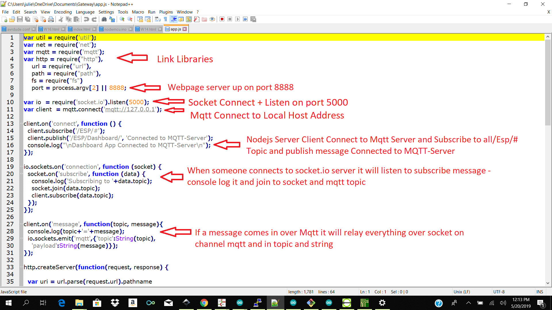
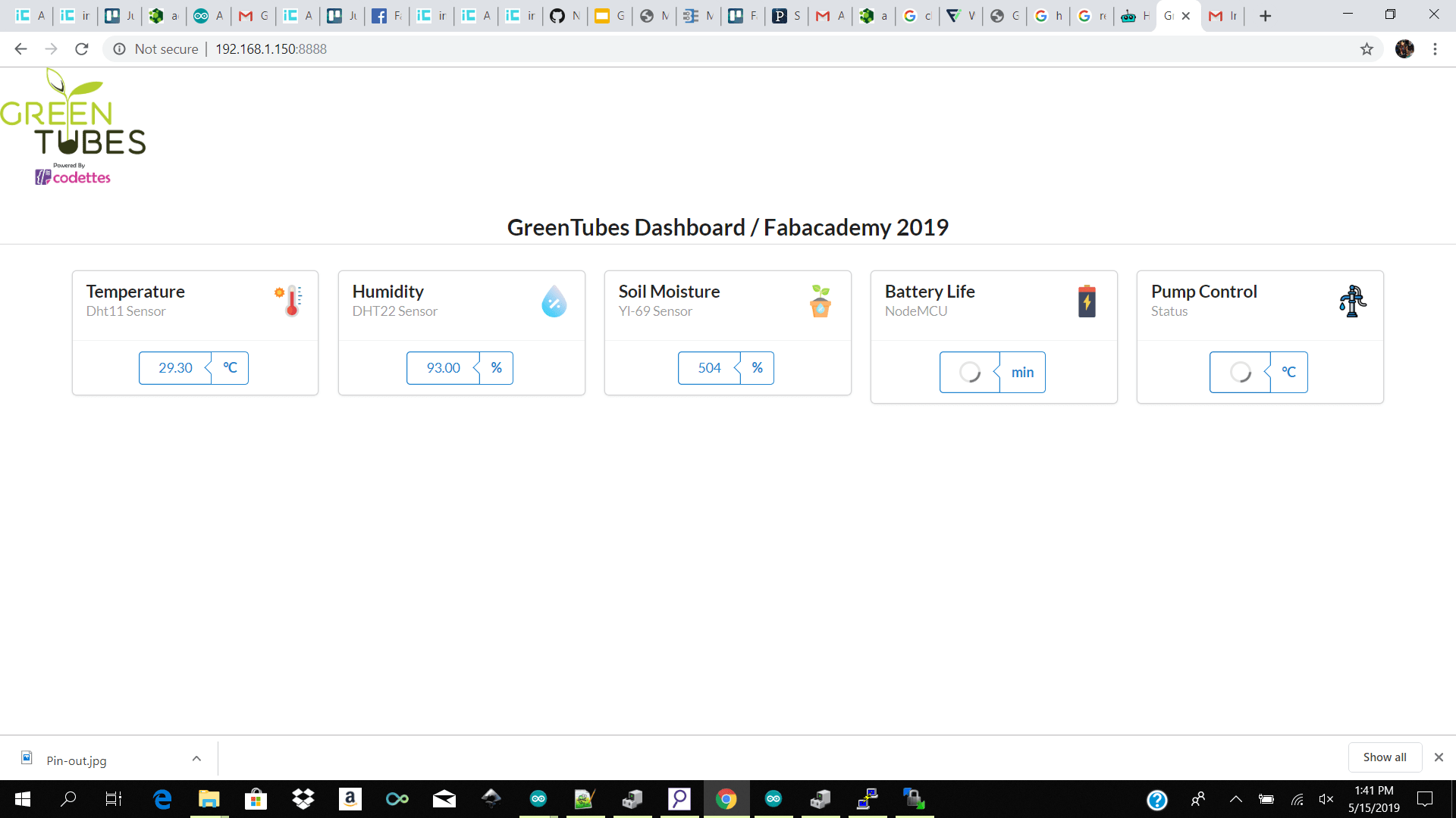
GATEWAY ON RPI3
For my first test I had nodejs (express socket.io )and mosquitto installed on my gateway (Raspberry pi 3 ) and I made a simple dashboard with 4 widgets for showing my sensor data.
Tools/ Reference
Folder Structure
- node_modules
- public
- css
- img
- js
- index.html
- app.js
- package.json
- package-lock.json
Code Structure
app.js
index.html
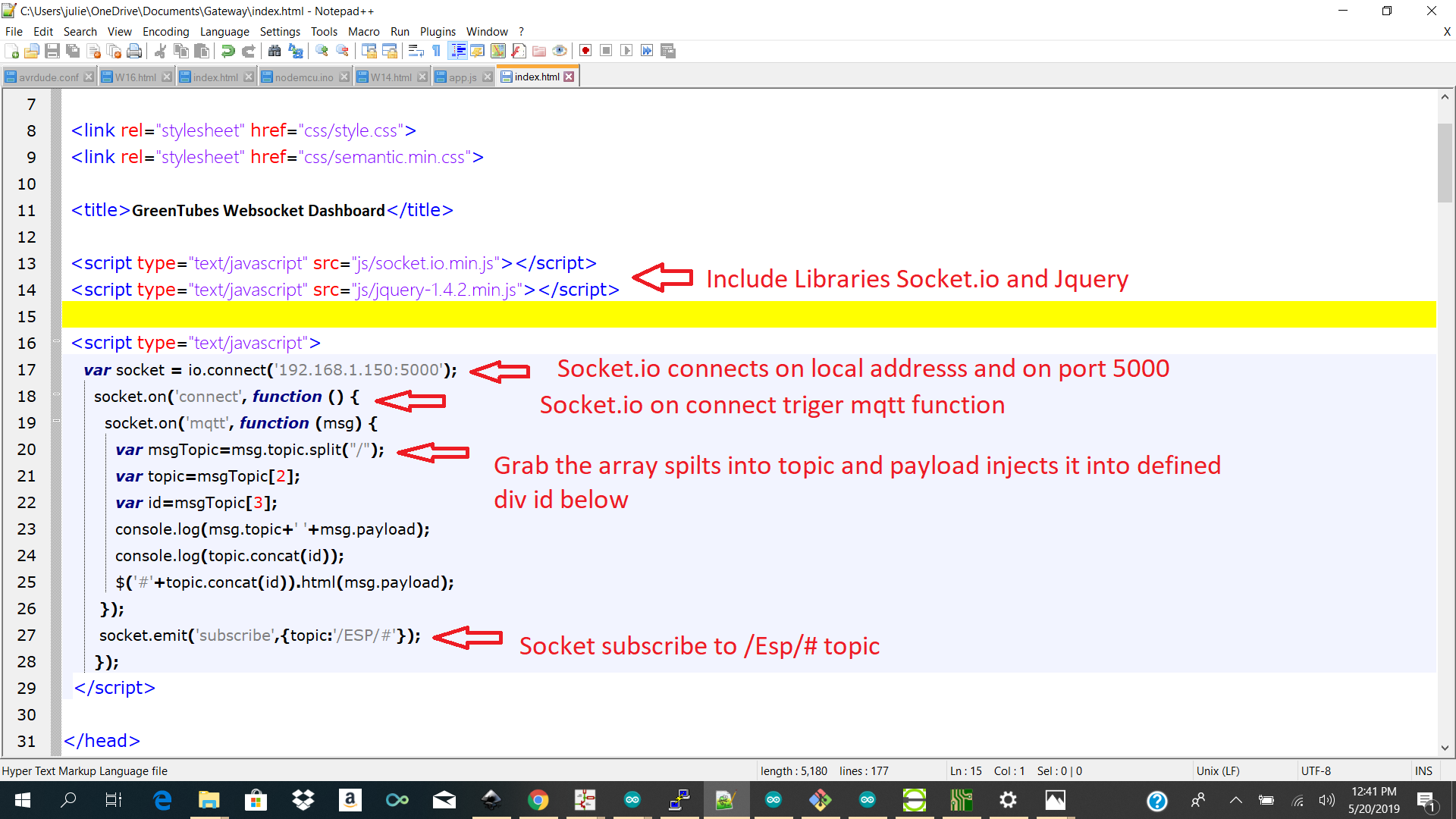
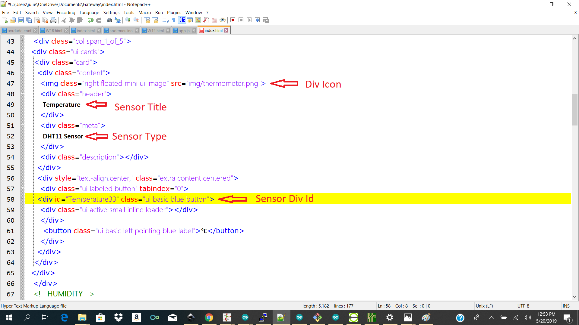
Dashboard
Problem
note: I had to manually install express and edit the app.js file to use express to route my path to find my css files and js files properly. I also moved all my files into a folder call public so that my route could find them. Component list
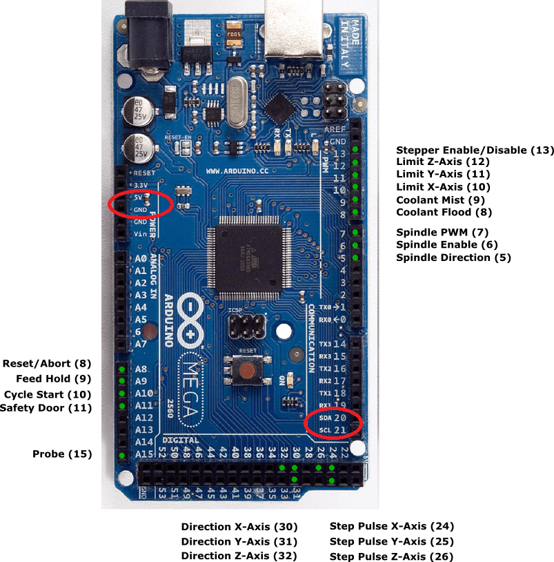
Arduino Mega and Arduino Uno i2c
Arduino uno / Arduino Mega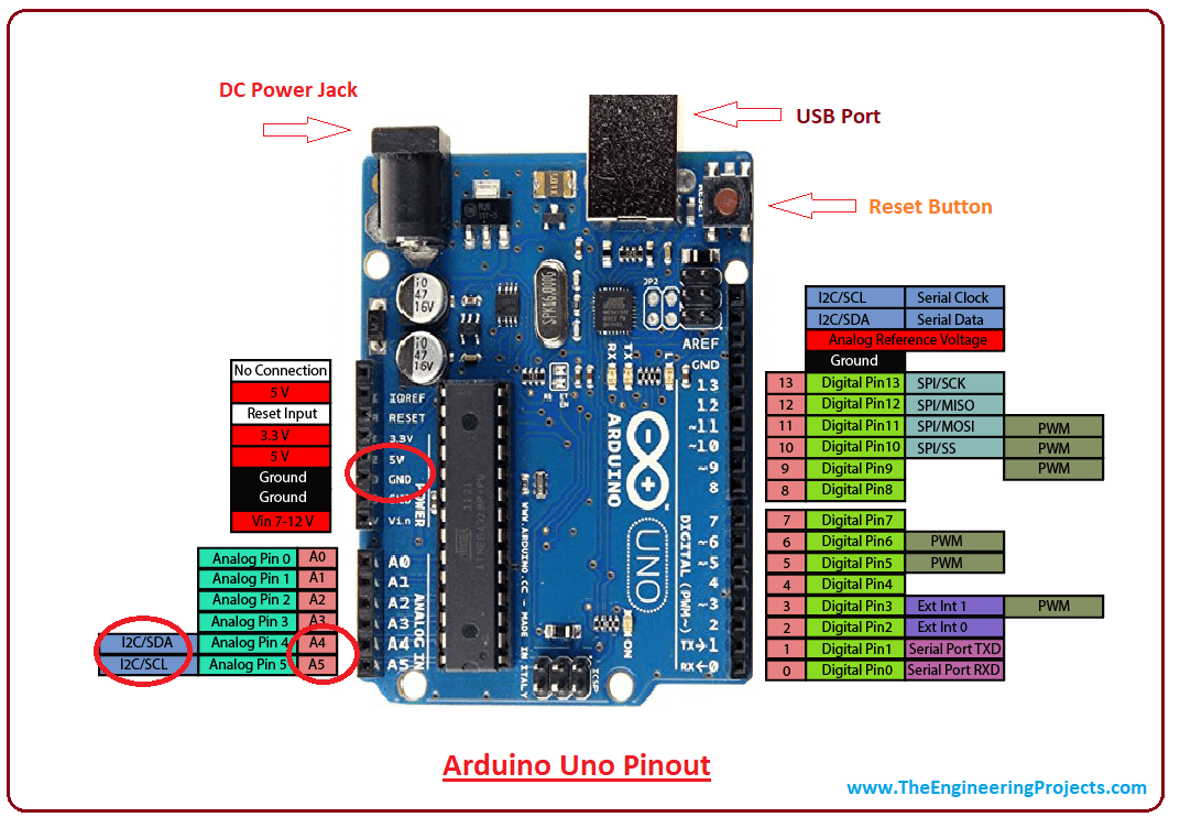
Arduino Uno and Attiny 44a i2c
Arduino uno / Attiny 44a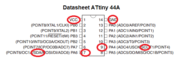
Arduino Uno and Attiny 45a i2c
Arduino uno / Attiny 45a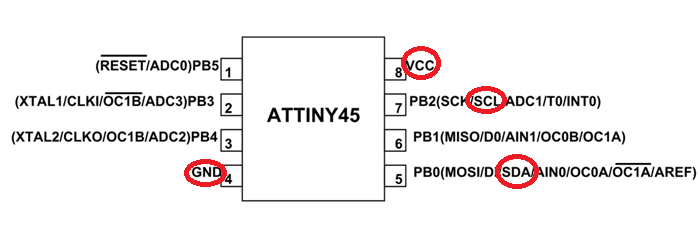
Attiny 45a Attiny 45a i2c
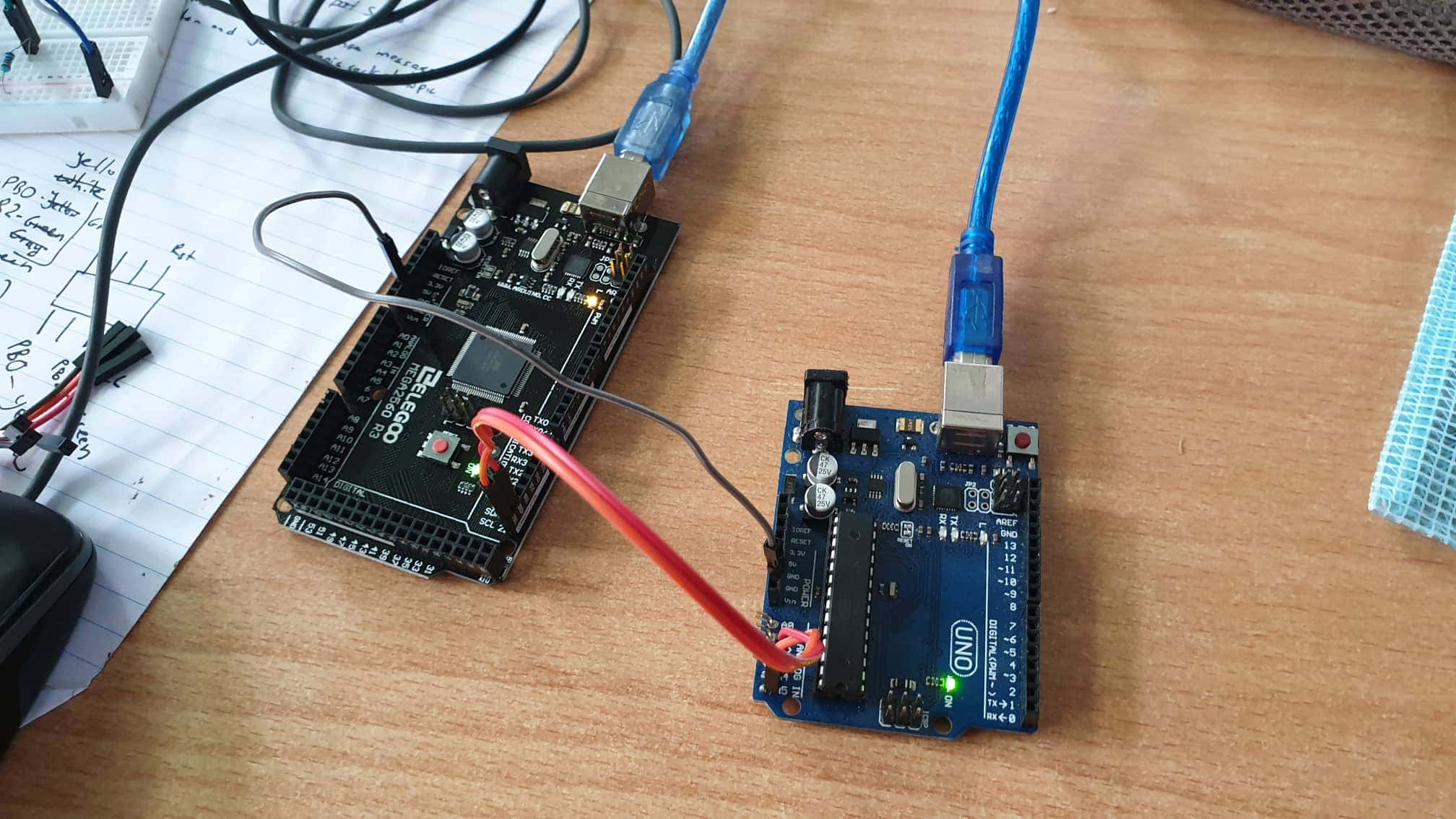
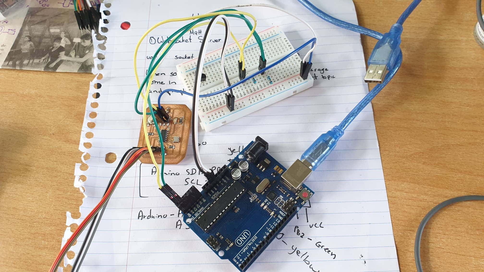
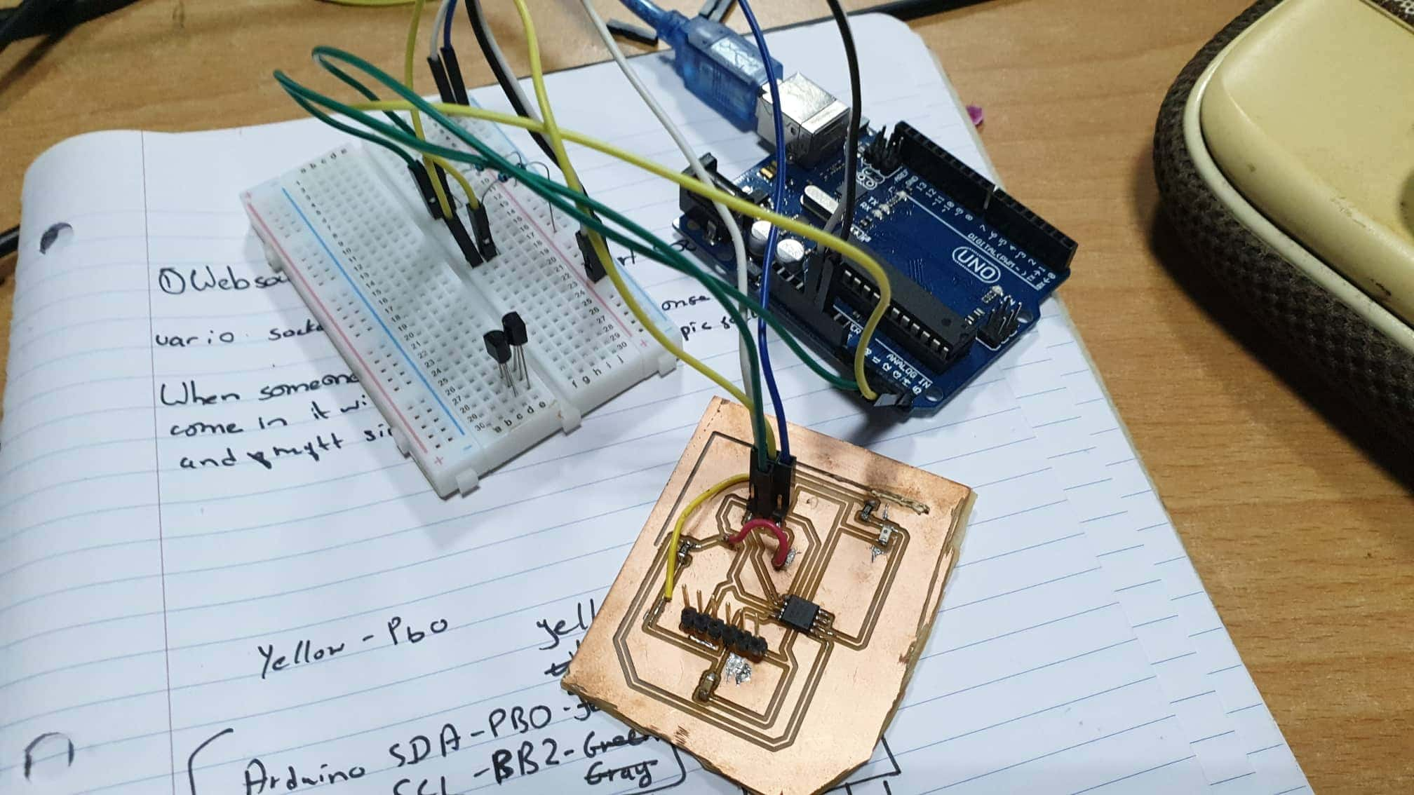
Attiny 45a Attiny 45aFor my first test I powered the slave attiny using the arduino mega 5v so I had a breakout cable attached the power and gnd from the mega to the power rail and use the gnd rail to common ground both of my attiny.
I then pull my common ground cables to my attiny header pins. I then power my master attiny board using the ftdi cable and powered my slave attiny using the power rail of my breakout board which was coming from the 5v from the arduino mega.
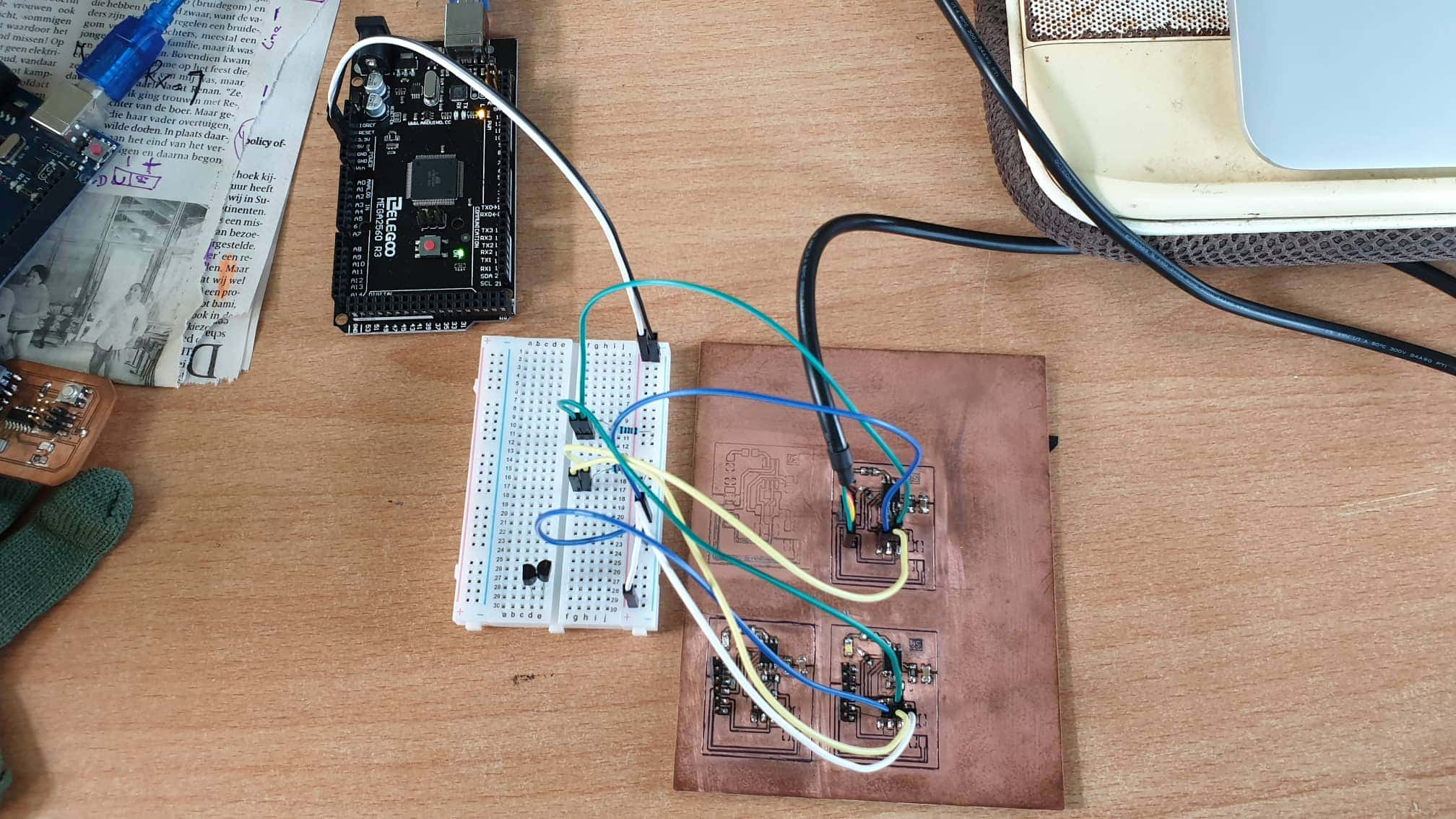
After doing a few tests with the arduino uno and mega and testing with the exsisting attiny 44 and 45 controller boards I had at hand and the i2c communications work I went ahead and started designing my board in Kicad.
I am going to be making 3 nodes. One will be acting as the master and the other two slaves.
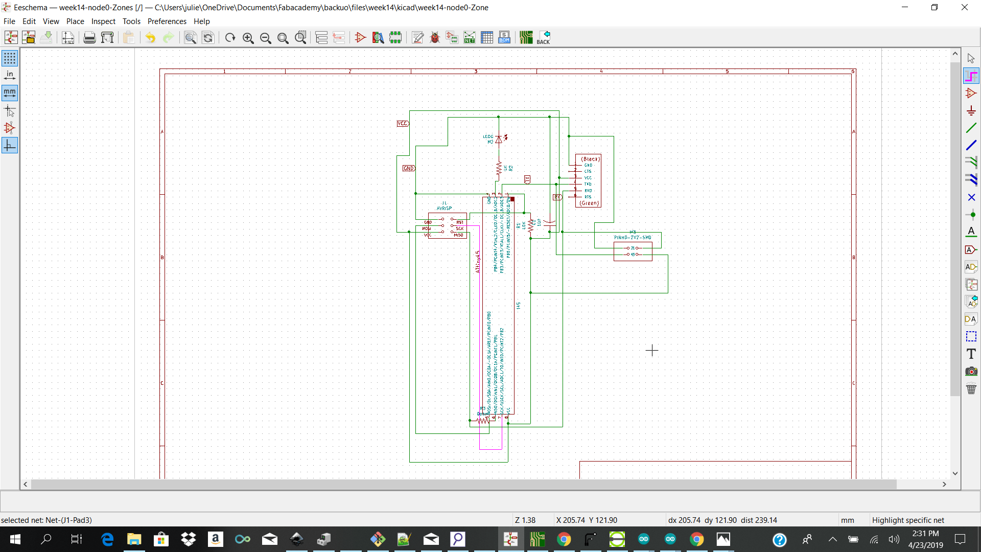
I made a new project and started selecting my components from the fab library. My baseline was the design which I made for my input week board using the attiny 45 controller.
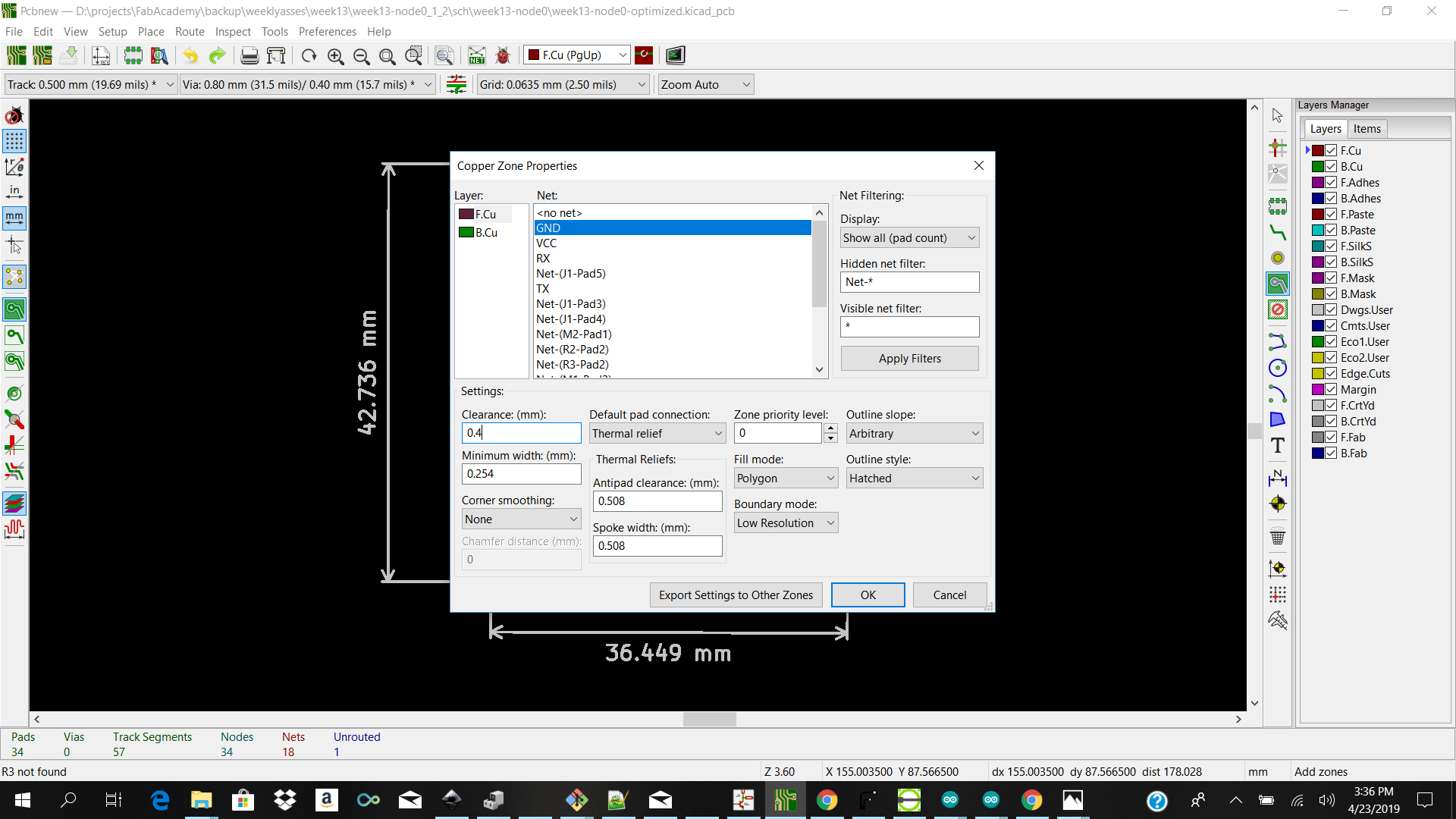
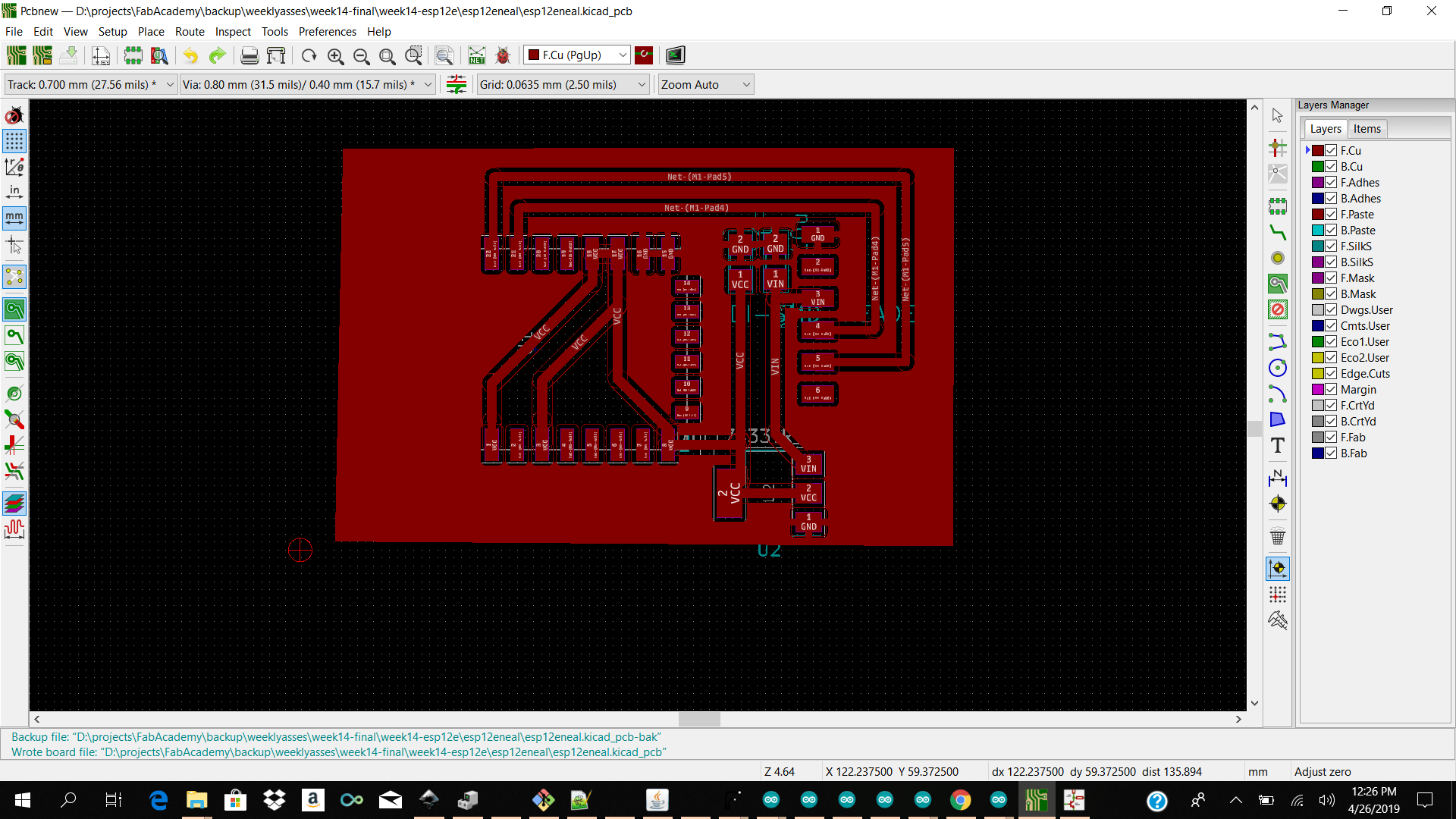
After making my schematic in kicad I went ahead and anotate to check if I had my tags labeled correctly. After that I went ahead and selected assign footprint to pcb and added my footprint. note:I used the fab 2x2 smd connector. I then selected on Generate netlist and imported my netlist for Pcbnew. I then went ahead and choose my design rules from Setup → Design rules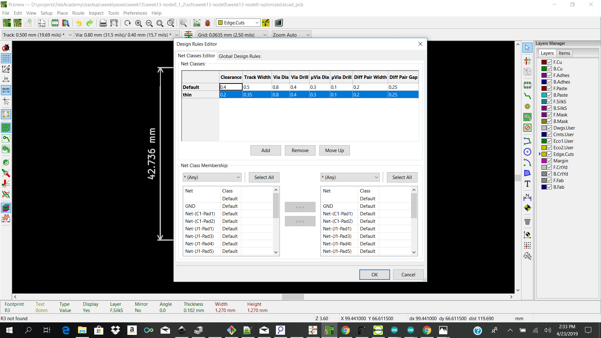 This time around I tried to used what ive learnt to try and optimize my design. I tried to make my board smaller so I waste less copper board.
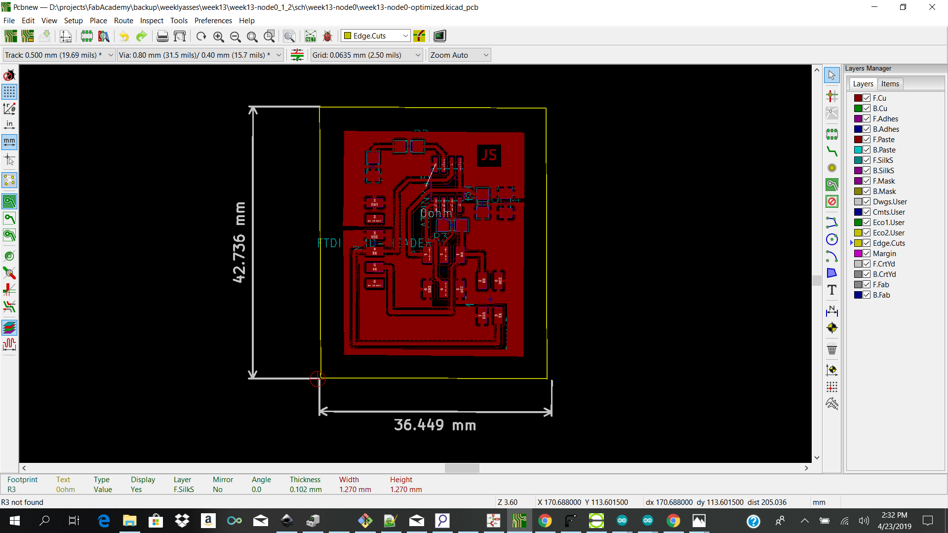 I also used the gnd and vcc planes so I dont need to make too many traces which would take less time to mill.
 I then determined my auxillary origin using the place the auxiliary origin icon and went ahead and plot my layers. When plotting I checked off both front and edge cut but I ended up not cutting out my board but have them all on one board.
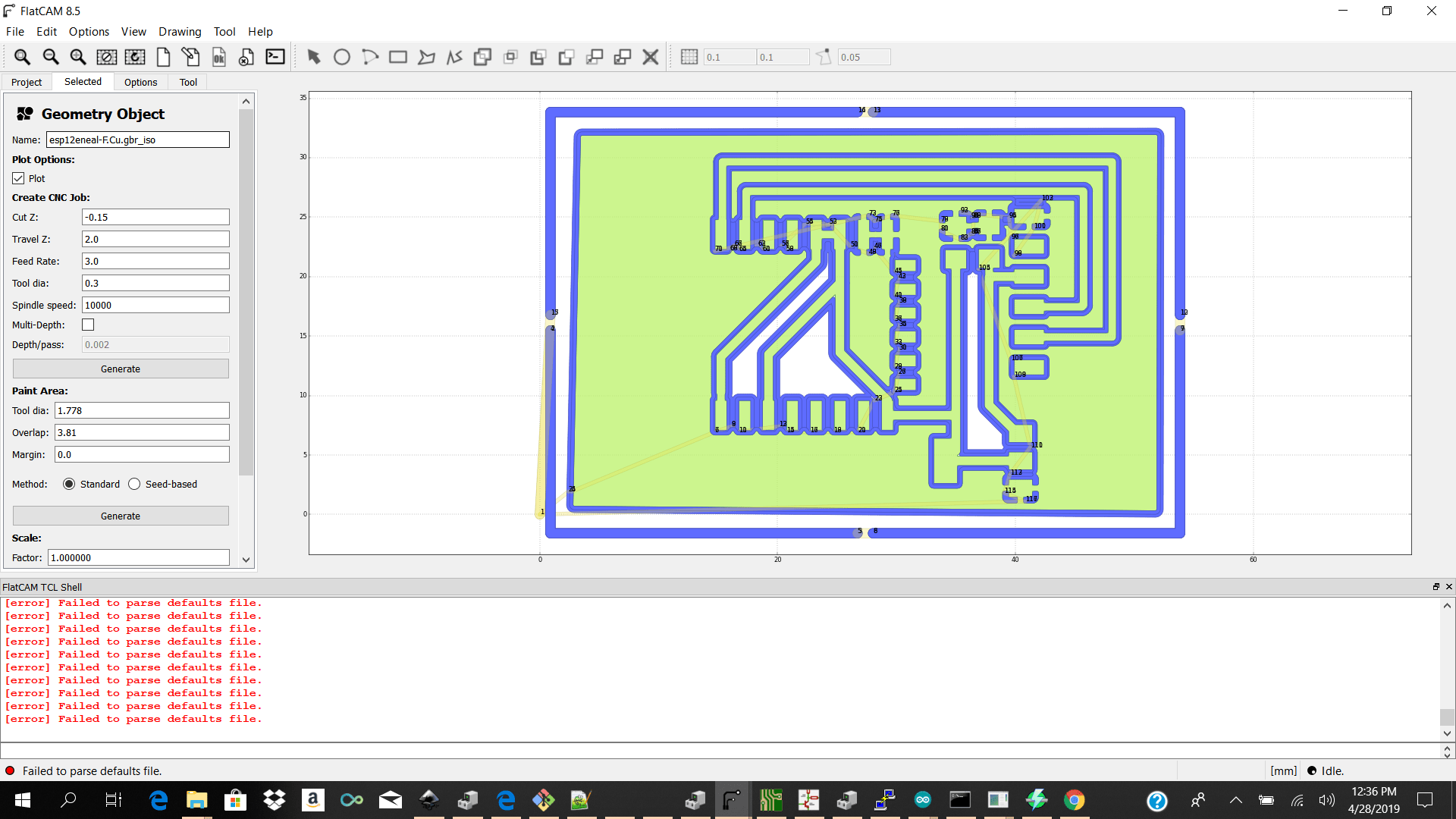
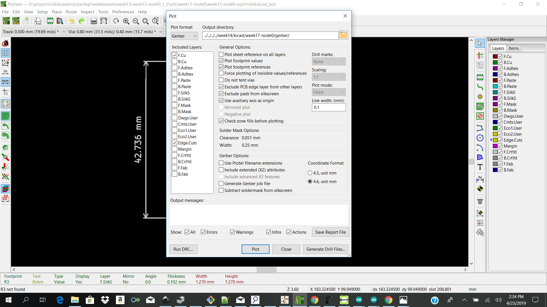 After generating my gerber files I then went ahead and open flatcam to add my parameters.
For the front cut I selected
After generating my gerber files I then went ahead and open flatcam to add my parameters.
For the front cut I selected
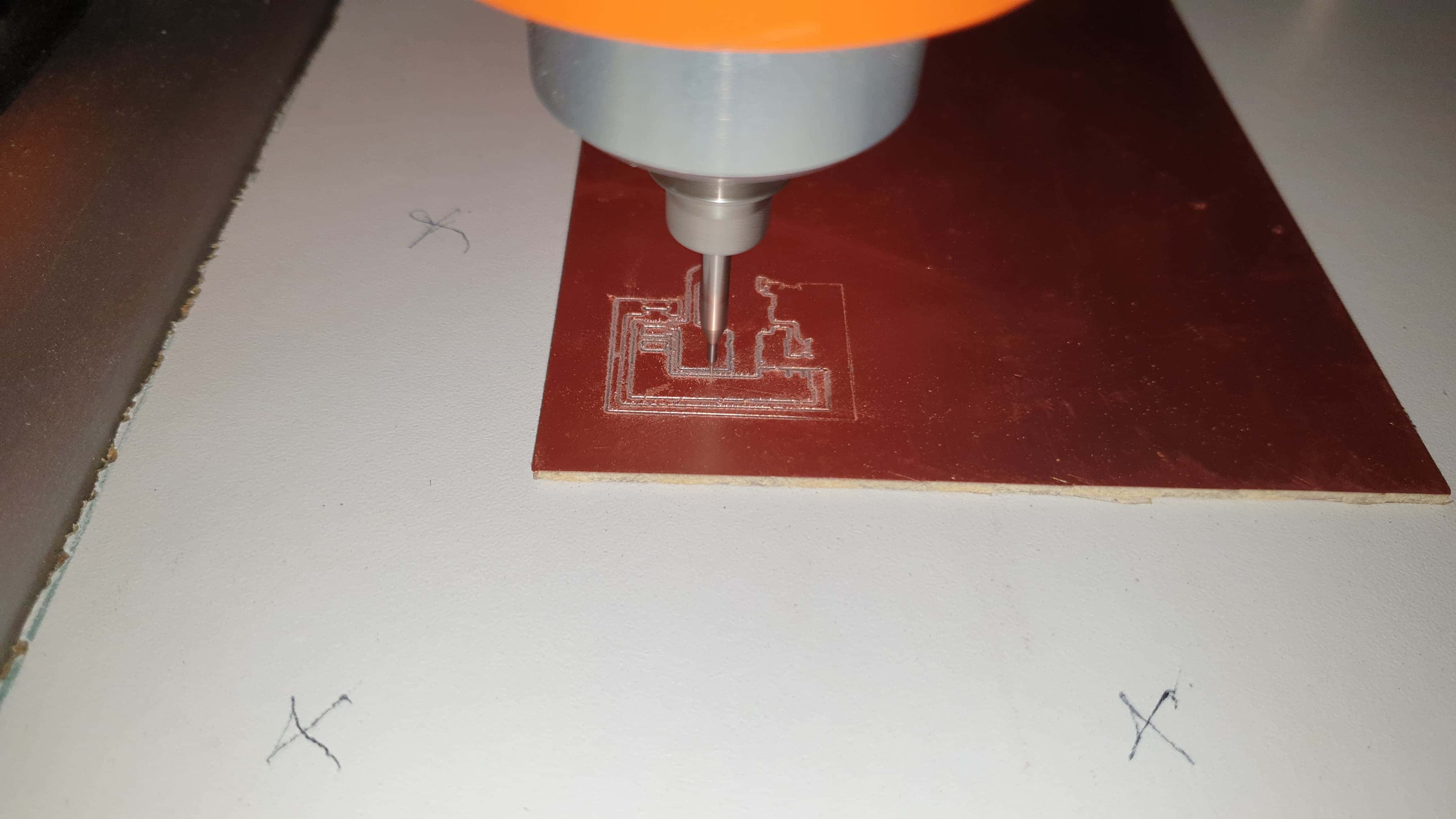
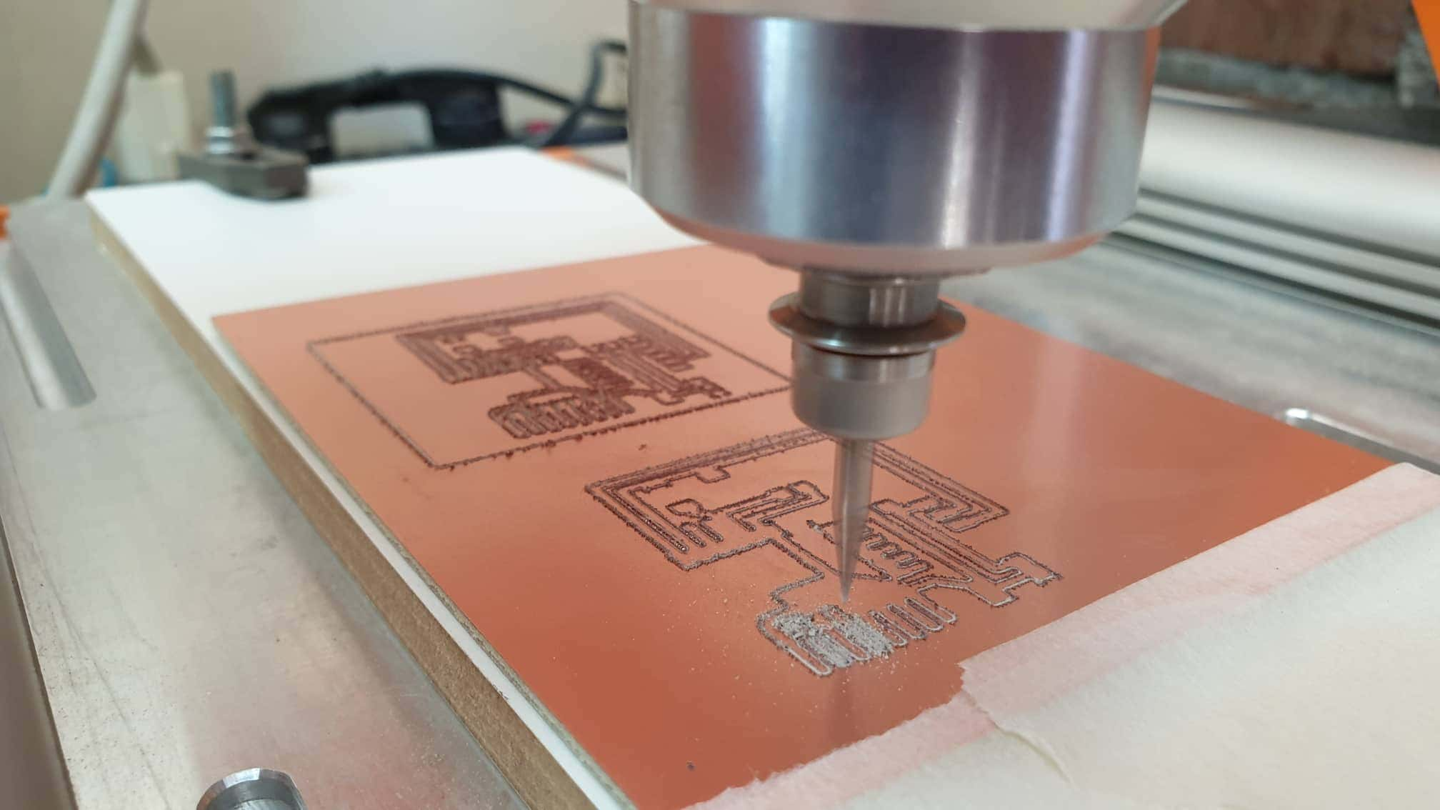
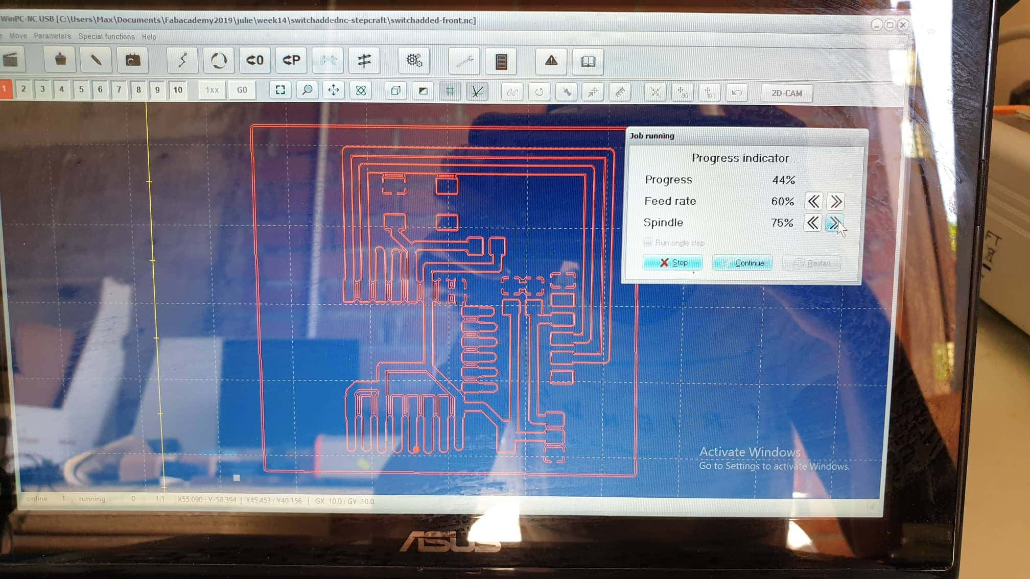
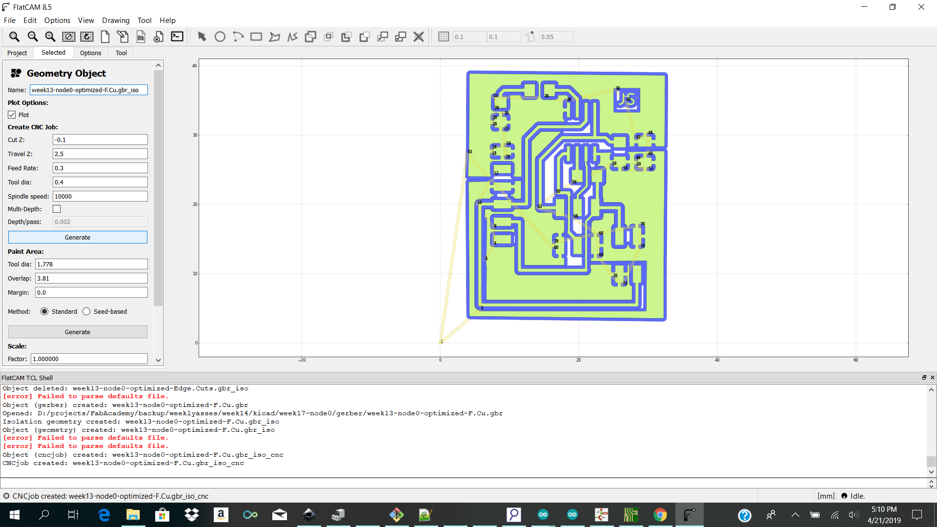 I then went ahead and generated my nc files for importing into winpc nc to control the stepcraft to cut the pcb.
Machining Wired Nodes
I then went and physically placed my copper plate onto the stepcraft base plate using double sided tape and imported my front cut.nc file into winpcnc. The parameters I had to keep in changer were add under Parameters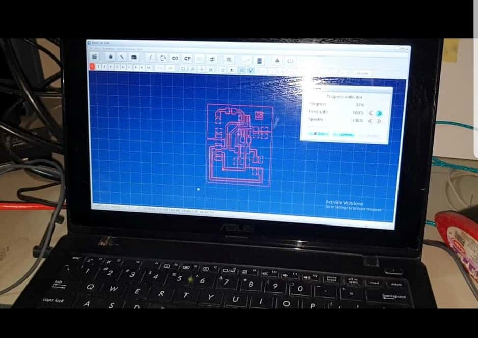
Soldering Wired Nodes
Soldering
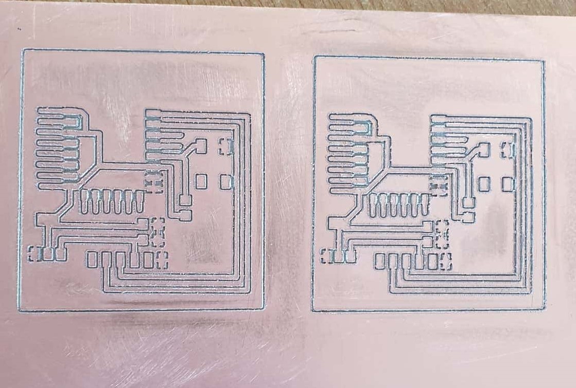
When milling my board I was using a broken bit which still had a good piece of bit left because we ran out of non broken bits so the bit started digging my traces and leaving rough copper flakes on my board. I DO NOT RECOMEND DOING THIS. I also used a smooth sandpaper to sand out the copper flakes and I took the multimeter and checked my connections if all that needs to be connected is connected and all the does not need to be connected is not and it was good. I then went ahead and gathered my smd components and sensors and soldered my board.
I started off soldering my microcontroller resistors capacitor and avrisp compoents to check if my conections are good and if I can burn my bootloader.note:I decided to mil all 3 of my boards on one board
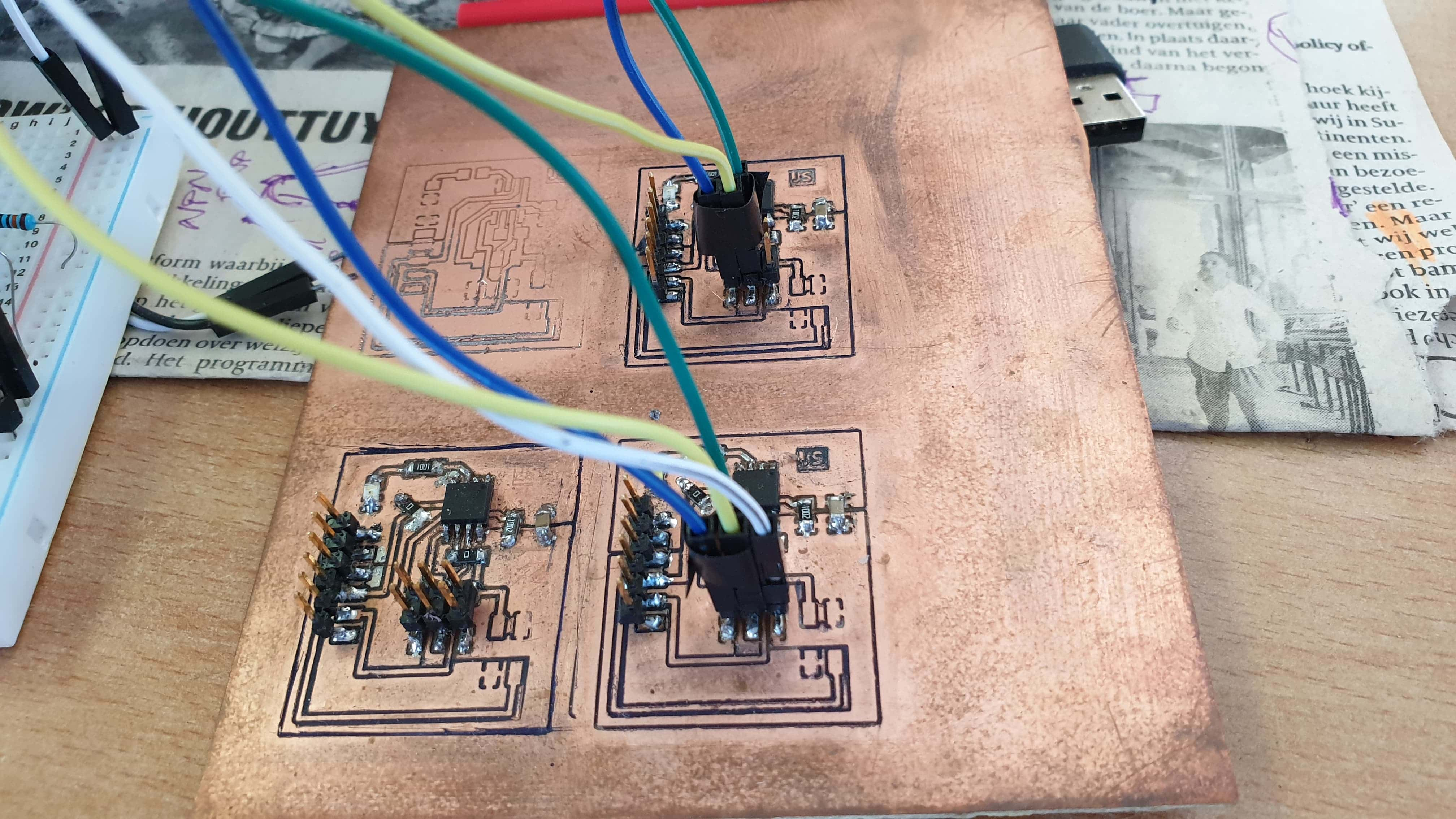
After having some issues with my connections bridging because of my broken bit I did some clean up of my board using a knife and eveything worked.
Lessons/Problems Summary
If your board has rough cuts and you have copper flaskes make sure to clean the traces before soldering orsled they will bridge your conections.
Programming Wired Nodes
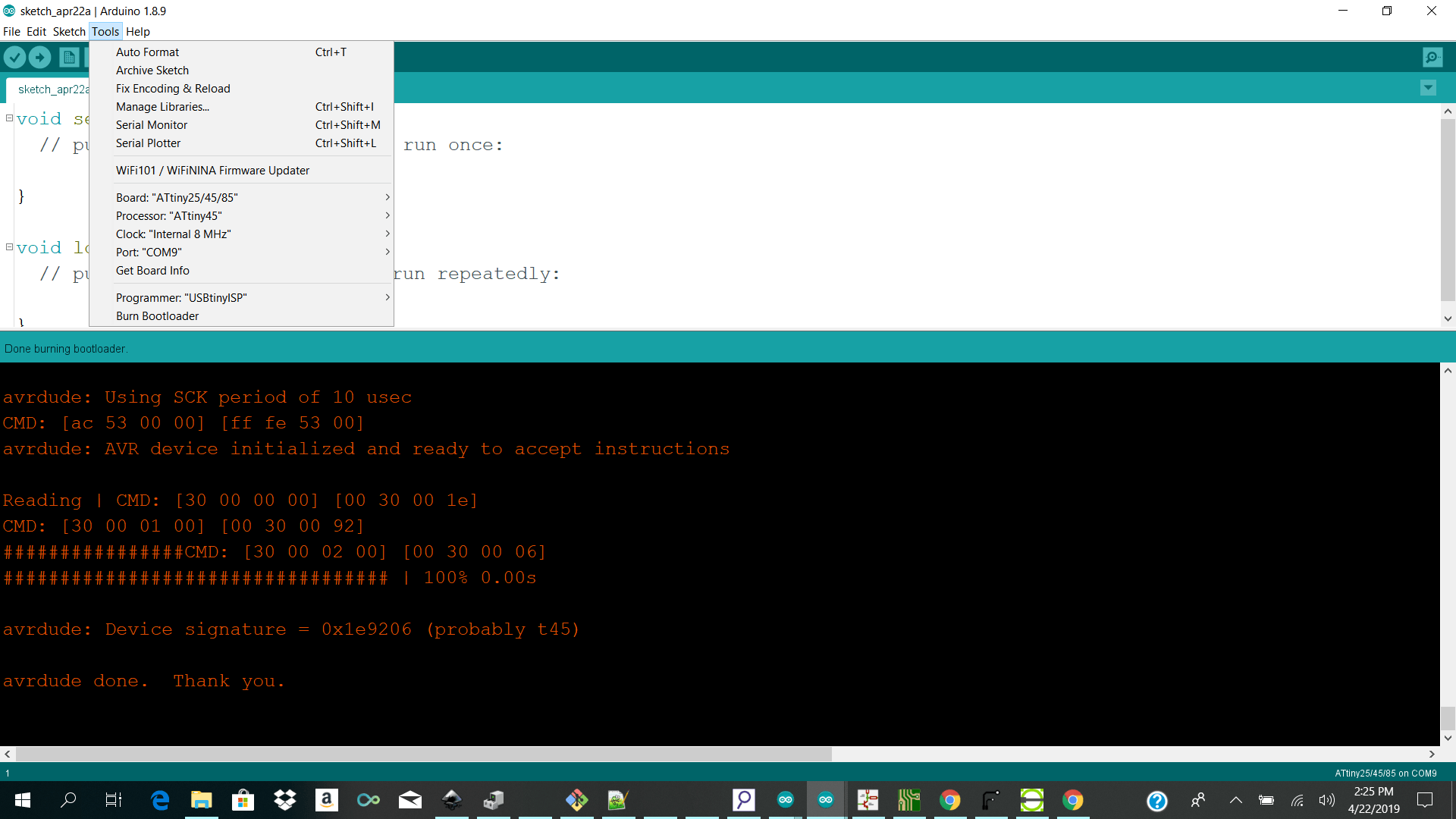
After soldering my attiny 45 with my resistors and capacitor board I went ahead and programmed it. The first test which I did and connect the fab isp to my computer and burn the bootloader using the arduino ide. I had already have the attiny core library installed from the previous week so I selected the
I then uploaded a simple blink led sketch to turn the leds of the attinys on and offpin 3 of the attiny 45a which maps to pin 4 of the arduino
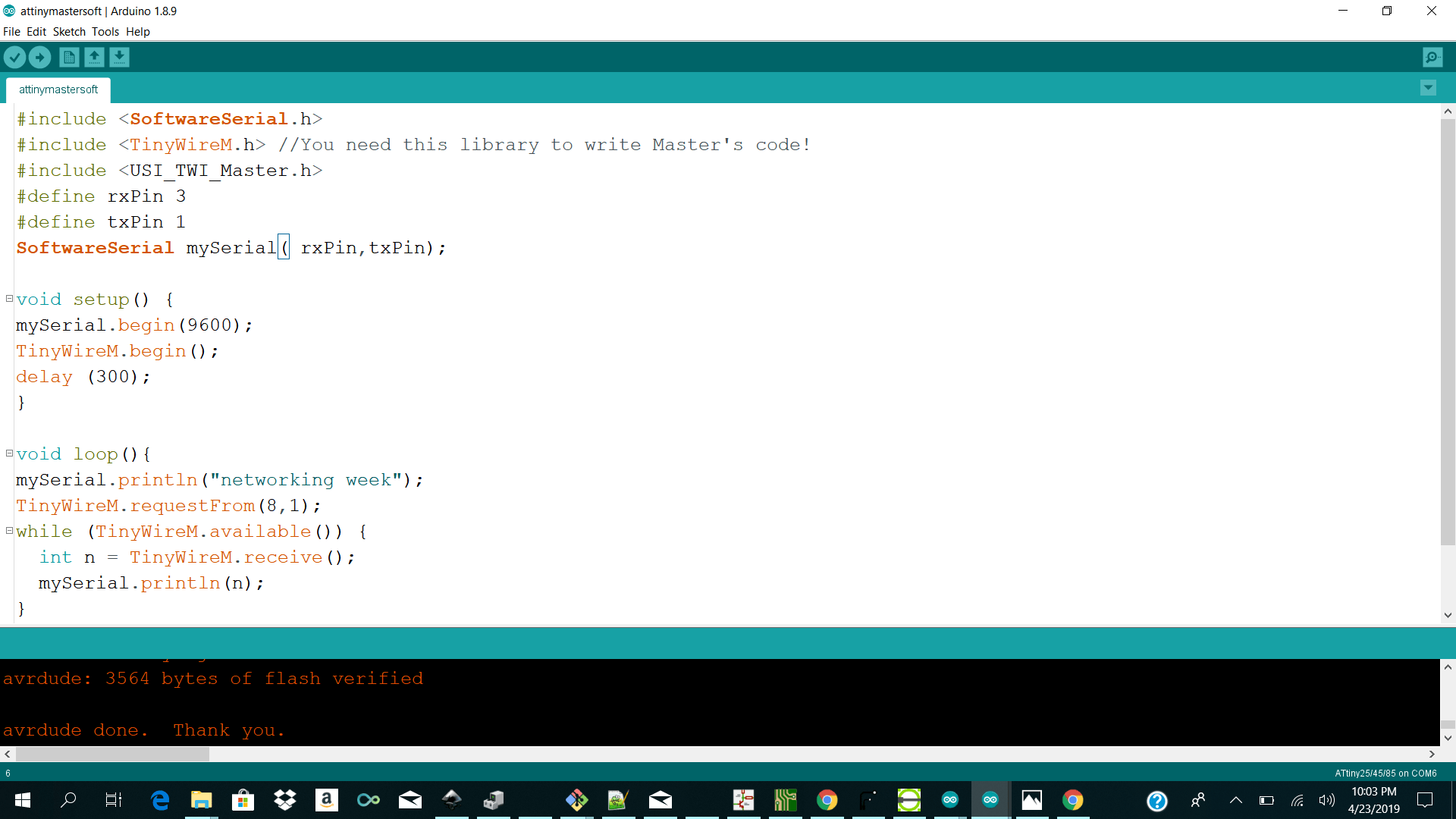
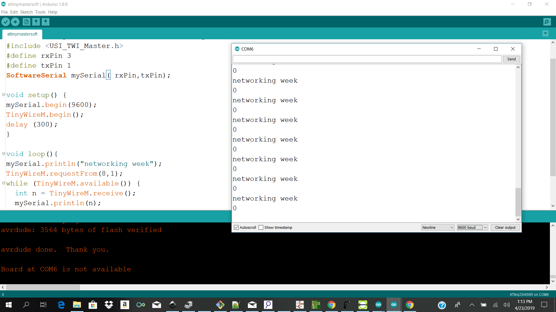
My next test I wanted to have the master attiny commuicating with the slave attiny by on starting of wire to send send a byte or command over and have the slave attiny send a response of a byte back over to the master and then read the data on the arduino ide serial monitor so therefore I would also need to have Software Serial library on my master attiny to map the rx and tx pins.
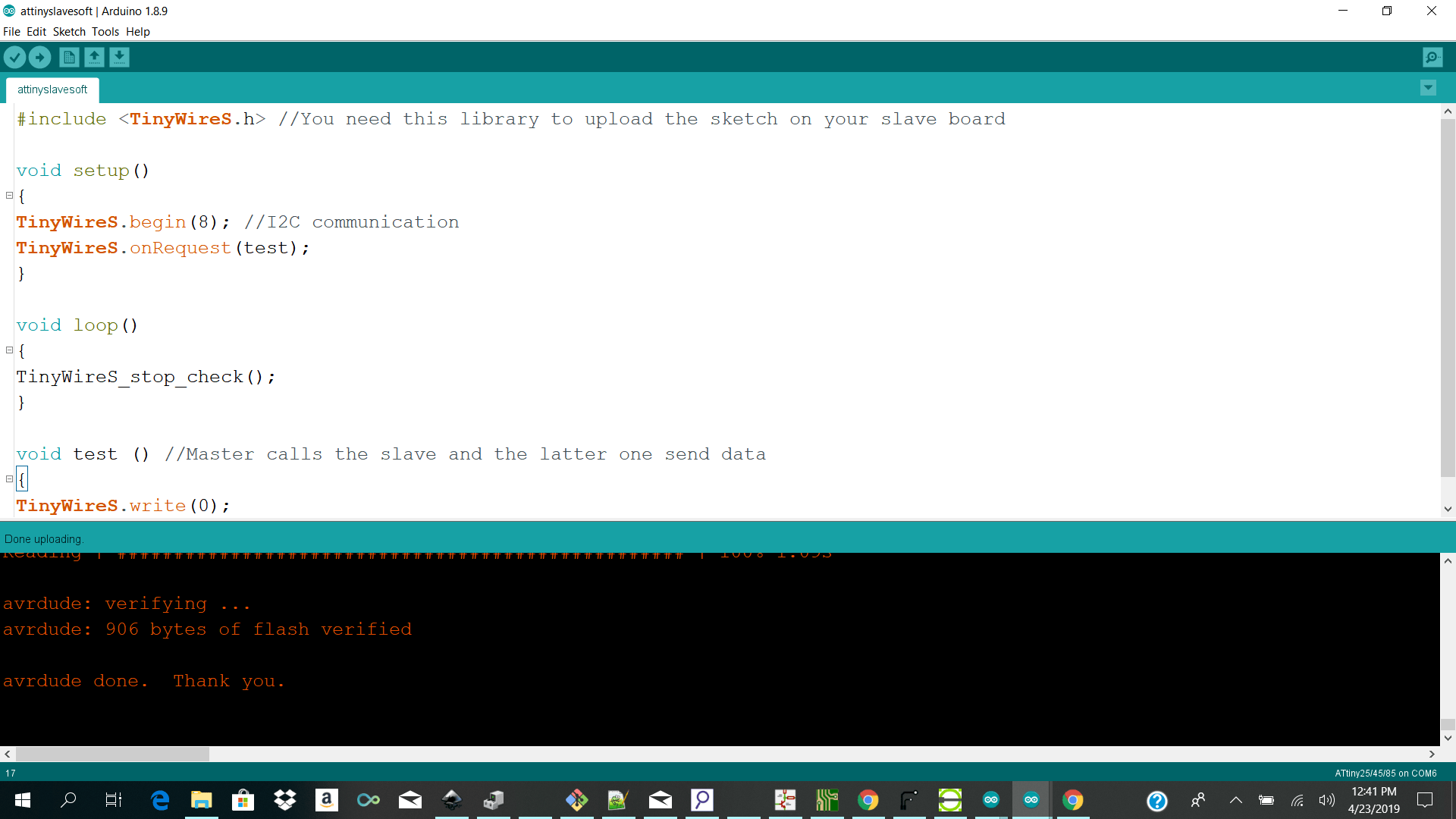
I initially used the tinywire.m library and the tinywire.s library to for my attiny master and slave codes but I kept getting errors saying a certin function no longer exsisted for the TinyWire.S library so I left it for a while then I found the TinyWire Library which worked for both the master and the slave. After doing some tests I realized that when I tried compiling my code using the TinyWire and Software serial I get this error which says vector -2 thing which I sdid not understand so I went back and tried the to compile using the TinyWire.m library and it compiled and I went back and tried the TinyWire.S library and still got the function issue so I went and checked what was actually in the library. When I opened up TinyWire.S library I saw they were using WRITE instead of SEND so I changed my code to TinyWireS.write(0); instead of send and it compiled perfectly.
The first sample test which I did was referenced from a pervious fab student fab student
In his code he was using I the software serial library to speak to the attiny hardware serial. He then defined my rx and tx pin (reverse the pin num rx goes to tx n tx to rx). I defined my Led pin that is attached to which was attiny pin 3 arduino pin 4
AttinyMasterCode
He includes TinyWire.M library and starts tinywire and starts serial on baudrate 9600 and prints networking week to serial monitor of arduino ide.He then requests from slave address 8 one byte stores the byte as an integer in the veriable n and prints what is in that variable to serial monitor.
AttinySlaveCode
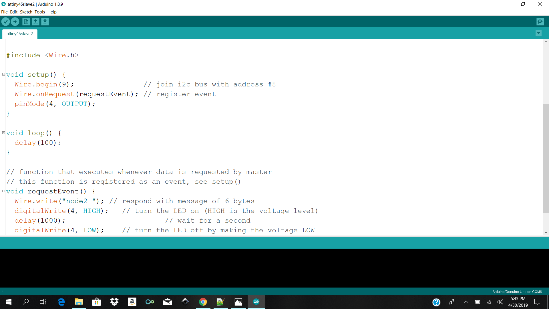
He includes TinyWire.S library and begins TinyWire.S on address 8 and on TinyWire.S request he starts a function and write the value 0 back to the master.
I tested his code out of the box and it worked perfectly so I got commuication from the master to one slave for my second test I will be writing my own piece of code to use one attiny as master to control two slaves to blink their leds and send the response back to the master sending strings and print the response on serial monitor.
Attiny i2c Test2 One master 2 slaves
The next step which I tried was to have one master receiving not just bytes from the slaves but a string.I had to do alot of reserach on byte to string conversion in C which was a hell because I was using the tinywireS and tinywireM libraries instead of the Wire library which worked fine.
In the end I realized that I could use the Wire for both the Arduino Uno Mega and Attiny 45 the only reason why I was getting conversion issues was because I was compiling my attiny code for the Attiny board instead of the ATTinyCore board.You can find it in the arduino ide board manager.
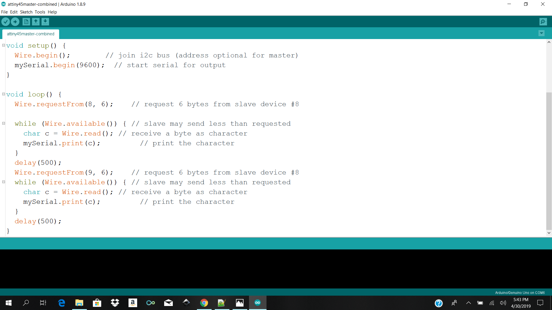
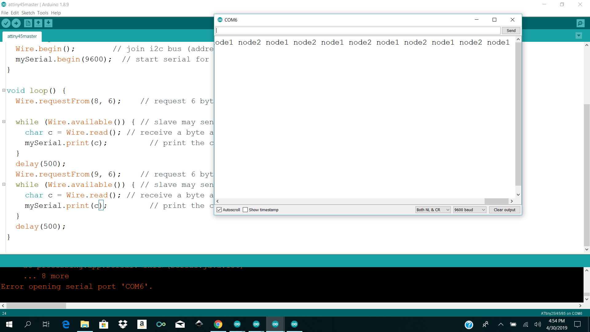
I then coded my master code opening transmission to my slaves on address 8 and 9 and to receive whatever is coming over serial which is char and convert it and print it to my serial monitor
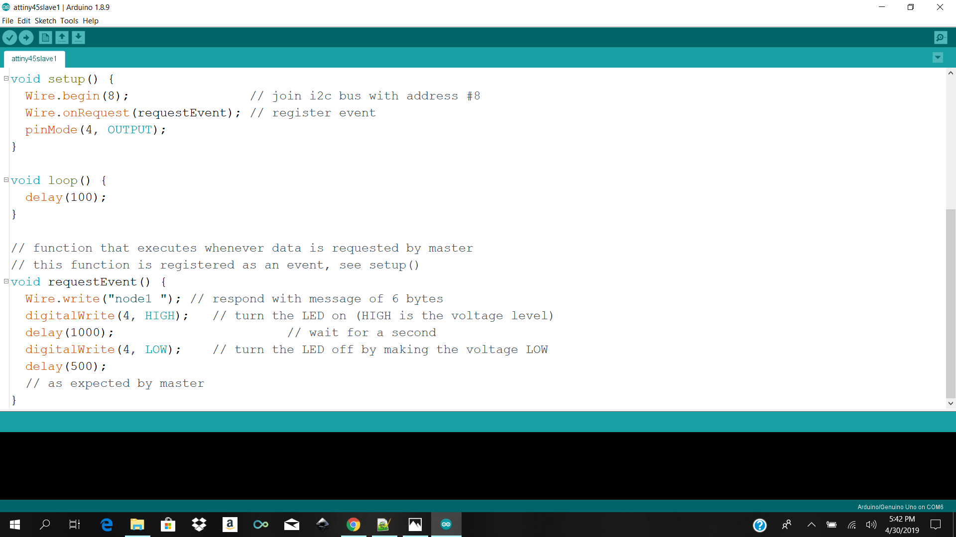
I then have my slaves doing the same thing sending their address to the master and to blink their leds on transmission the only difference is that one slave is on addess 8 and the other is 9
As you can see the master is receiving the response from node 1 and node 2 and printing it to serial
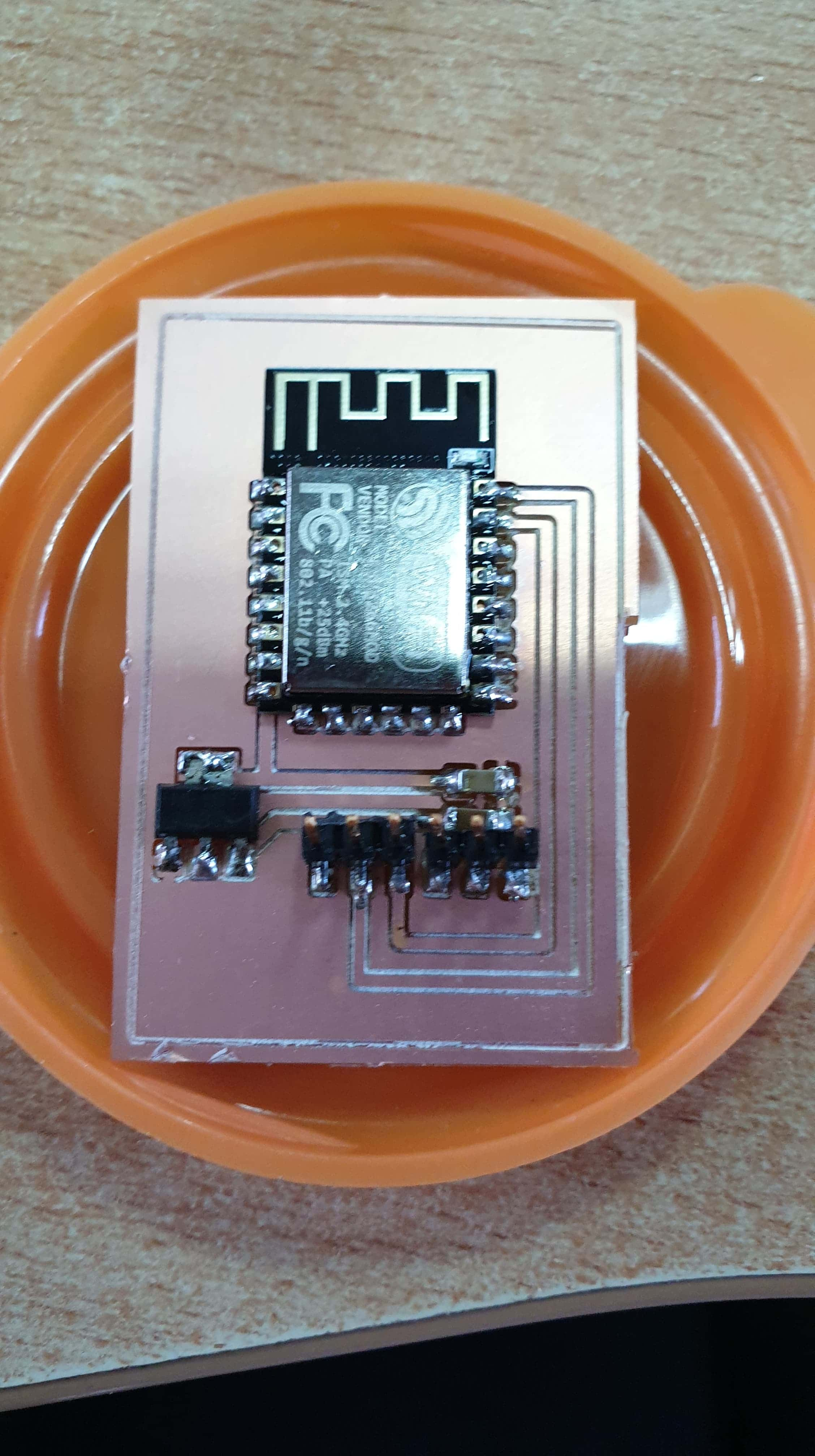
Designing Wireless Nodes
For my wireless node example I went along with neal design to check if i can get the esp8266 12 e to work because I will be neading this for my final prohject. Eventhough I went ahead with neal design I still redesign the parts in kicaed from scratch so I can have an idea of how to assemble my compoennts.
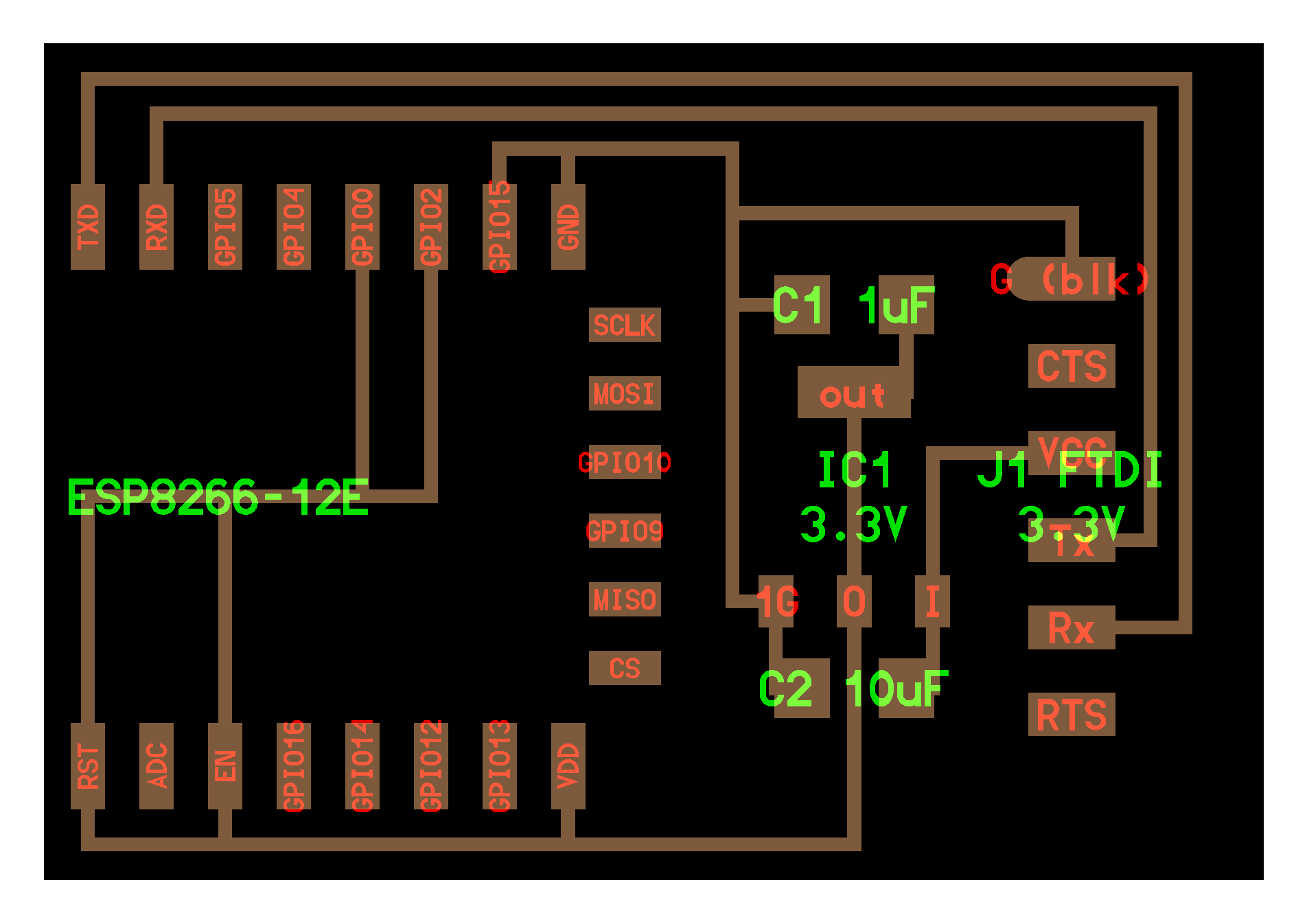
The steps are basically the same as above for designing the wireless node in kicad see above and below is my skematic and pcb new of kicad and my parameters of flatcam.The only thing which I changed in flatcam was going 2 passes instead of one and adding a overlap of 0.17 instead of 0.15
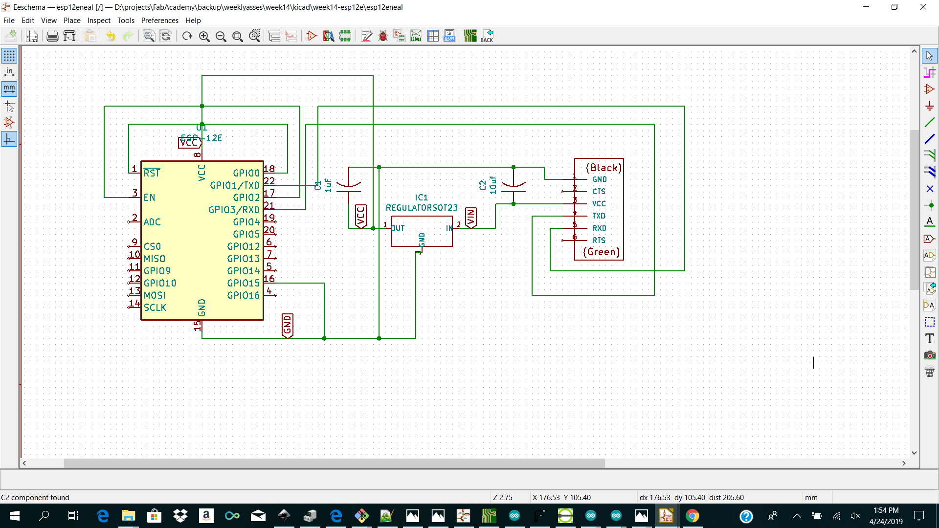 Note: I used the GND Plane for my design to make less tracks
 Note: The only issue I had with my design was to find the correct regulator for converting my voltage from 5 or 8 volt to 3.3 volt for my esp module.
We did not have a 3.3 volt regulator which outputs more than 100ma. I needed one which gives an output of 1amp. So I found some scrap electronics which was in the lab and desoldered a ME1117 3.3 voltage regulator and it worked beautfifully.
Note: The only issue I had with my design was to find the correct regulator for converting my voltage from 5 or 8 volt to 3.3 volt for my esp module.
We did not have a 3.3 volt regulator which outputs more than 100ma. I needed one which gives an output of 1amp. So I found some scrap electronics which was in the lab and desoldered a ME1117 3.3 voltage regulator and it worked beautfifully.
ME1117 Voltage Regulator
Soldering Wireless Nodes
Programming Wireless Nodes
After soldering and powering my esp8266 module I did some research and had to see if my esp8266 was responding to me. The way to do so is to power the esp up and connect the ftdi cable to it and plug it into my laptop running arduino ide
It was sugested to set the arduino ide to baudrate 115200 to send AT commands to the esp and 74880 to check the bootloader.
After trying a few times I was not geting a response so I decided to find a tool for flashing a new firmware unto the esp module you can get it below and I also downlaoded two firmare.bin files to flash the esp with. They both ended to be chinese and called fairy something.
I also had to redesign neils design to instead of pulling the gpio directly to vcc to add a 10k resistor and connect a button to it to pull the gpio 0 for it to be ready to be flashed.So programming mode. You can see the design below.
But before I went and milled my new design I just hacked the existing board which I had by cutting the gpio 0 from under my chip and adding a 10 k resistor to my esp pin and pulling a jumper cable to pull it to my gnd plane to put it into flash mode temperarly.
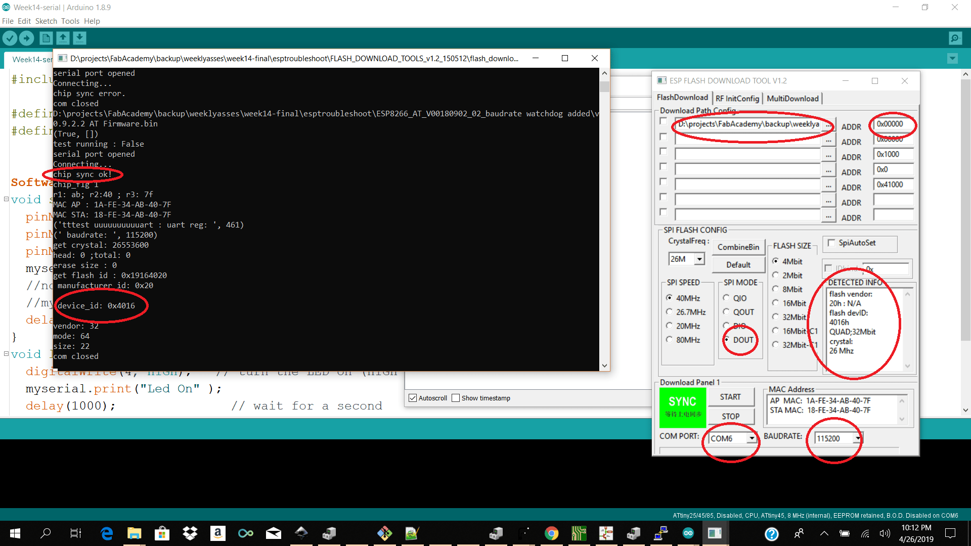
I could not find a login eventhough the esp broadcasted itself and was on ap mode. I then did some more research and relized that the esp sucked up alot of power and needed to not be powered by the ftdi alone. After powering the esp seperatly I got the response to check the bootloader from the esp on baudrate 74880
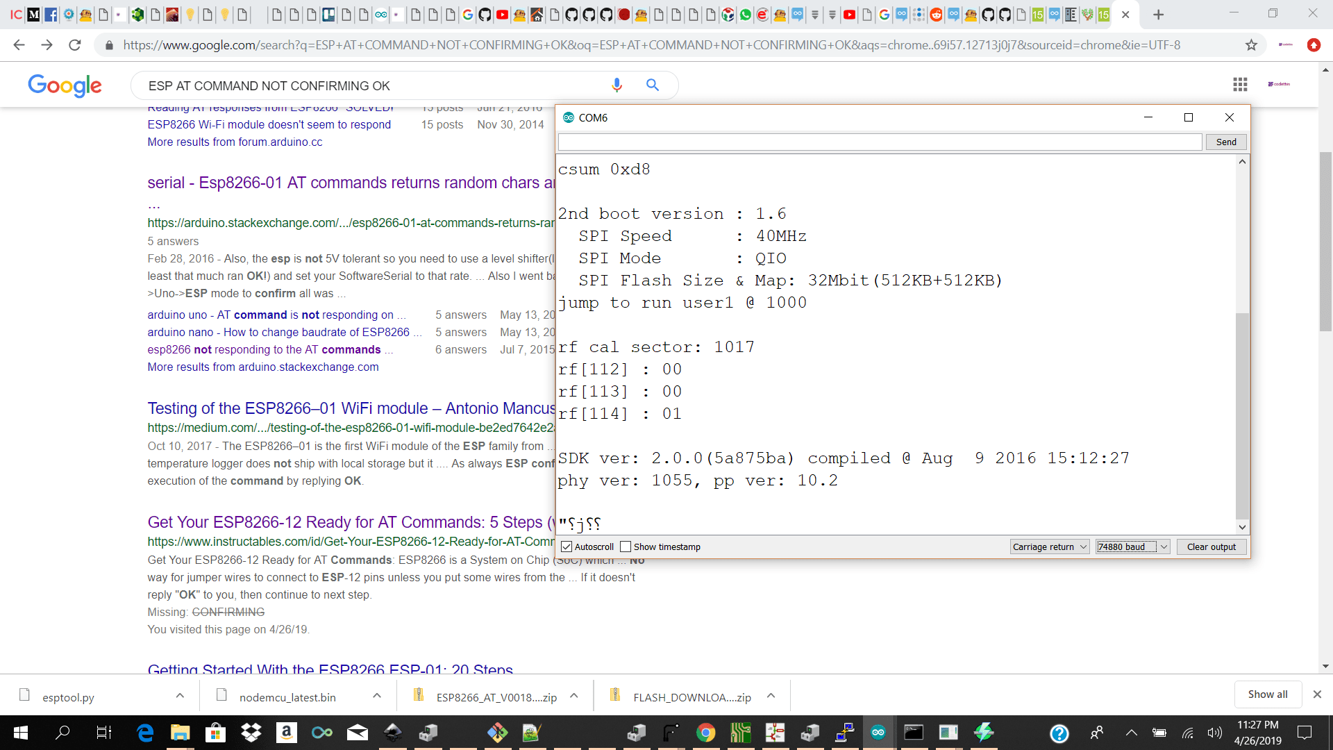
The next step which I had to do was to see if I can send AT to esp and get back and OK but that was no success I got no response.
AT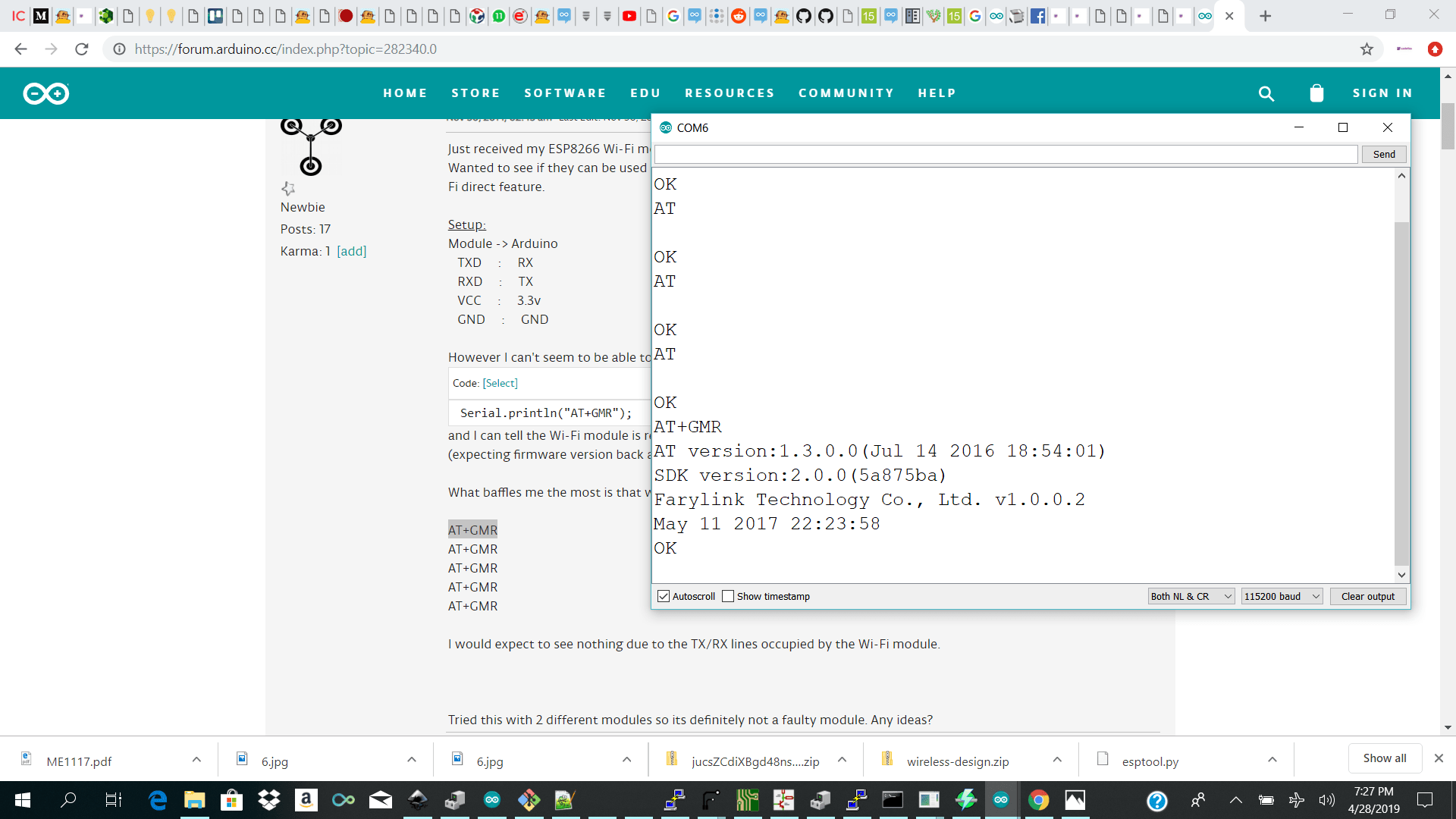
Download Links Here
Kicad Wire Nodes
Kicad Esp8266 Neal design + Optimized
MasterSlaveTest1 Zip
I2C Combines Master Slave1 Slave2
Flashtools
Contact Us
Where To Find Us
Paramaribo Suriname
Ethnalaan
50..