Designing
Summary
- Design Output Microcontroller Board
- Creat New Project & Sketch KICAD
- Import Fab Library
- Import Components
- Connect Components
- Give Compoents correct name and value
- Annotate the design
- Assign Footprint to Symbols
- Generate Netlist
- Open Pcb New
- Read in Generate netlist
- In Pcb New Set Design Rules (Setup -Design Rules)
- Rearrange Components and Make Traces
- Place your Auxillary Axis
- Plot Layers
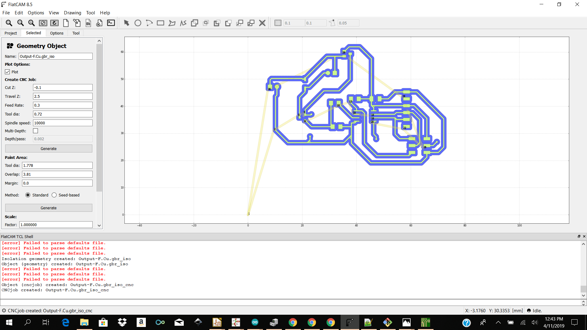
- Flatcam
- Physical tool dia 0.40 flatcam params 0.72 note:My initial intention was to use a 0.68mm bit so I needed to trick flatcam and putting 0.72mm for tool dia so that my tool goes into the small corners between my compoents but at last min the 0.68mm bit broke so I ended up using a 0.40 bit.
- Cutz -0.1
- Travel Z 2.5
- Feed Rate 0.3
- Spindle speed 10000
- Passes 1
- Solder Output Microcontroller Board
- Programming Output Microcontroller Board
Designing
For Output week I decided to make a microcontroller board using the attiny45 microcontroller and for my actuator I choose to use a dc motor.I also added the avrisp for programming my board and the 6 pin header for connecting my htdi cable to read from serial. Component list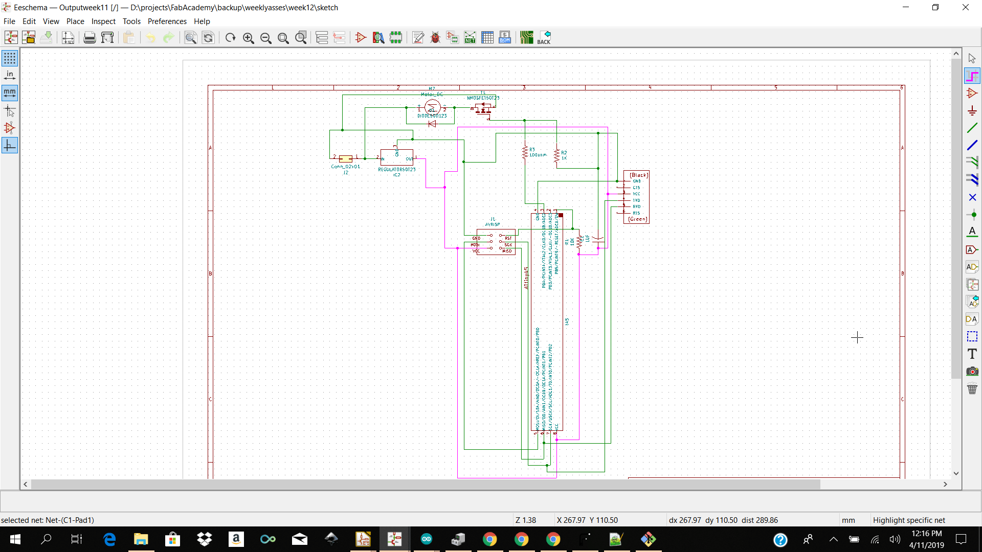 I then went ahead and started making my skematic in Kicad. I made a new project and started selecting my components from the fab library. I found most of my components from the fab library but I had to add my own library for the header pins for my motor and power connectors. After making my schematic in kicad I went ahead and anotate to check if I had my tags labeled correctly.
After that I went ahead and selected assign footprint to pcb and added my footprint. I had an issue with my conector pins footprint so I had to create my own footprint in pcb new. I then selected on Generate netlist and imported my netlist for Pcbnew.
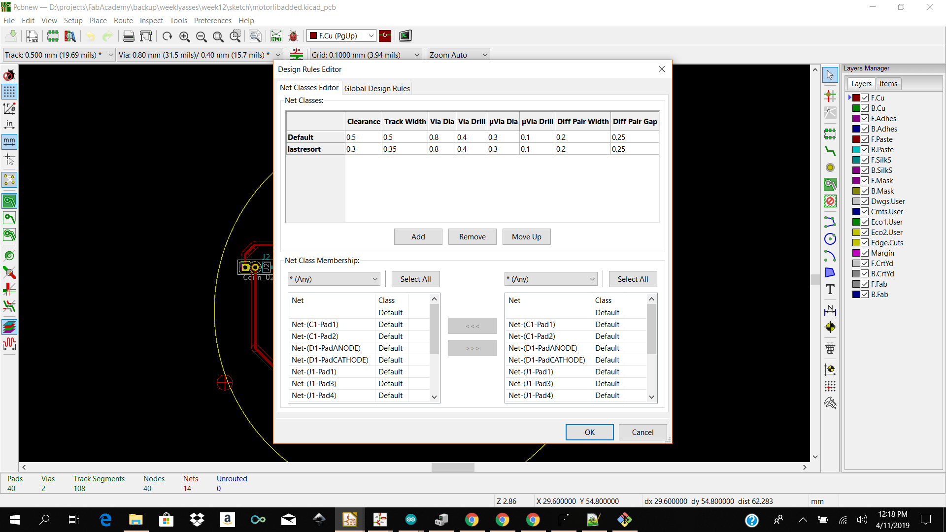
I then went ahead and choose my design rules from Setup → Design rules
I then went ahead and started making my skematic in Kicad. I made a new project and started selecting my components from the fab library. I found most of my components from the fab library but I had to add my own library for the header pins for my motor and power connectors. After making my schematic in kicad I went ahead and anotate to check if I had my tags labeled correctly.
After that I went ahead and selected assign footprint to pcb and added my footprint. I had an issue with my conector pins footprint so I had to create my own footprint in pcb new. I then selected on Generate netlist and imported my netlist for Pcbnew.
I then went ahead and choose my design rules from Setup → Design rules
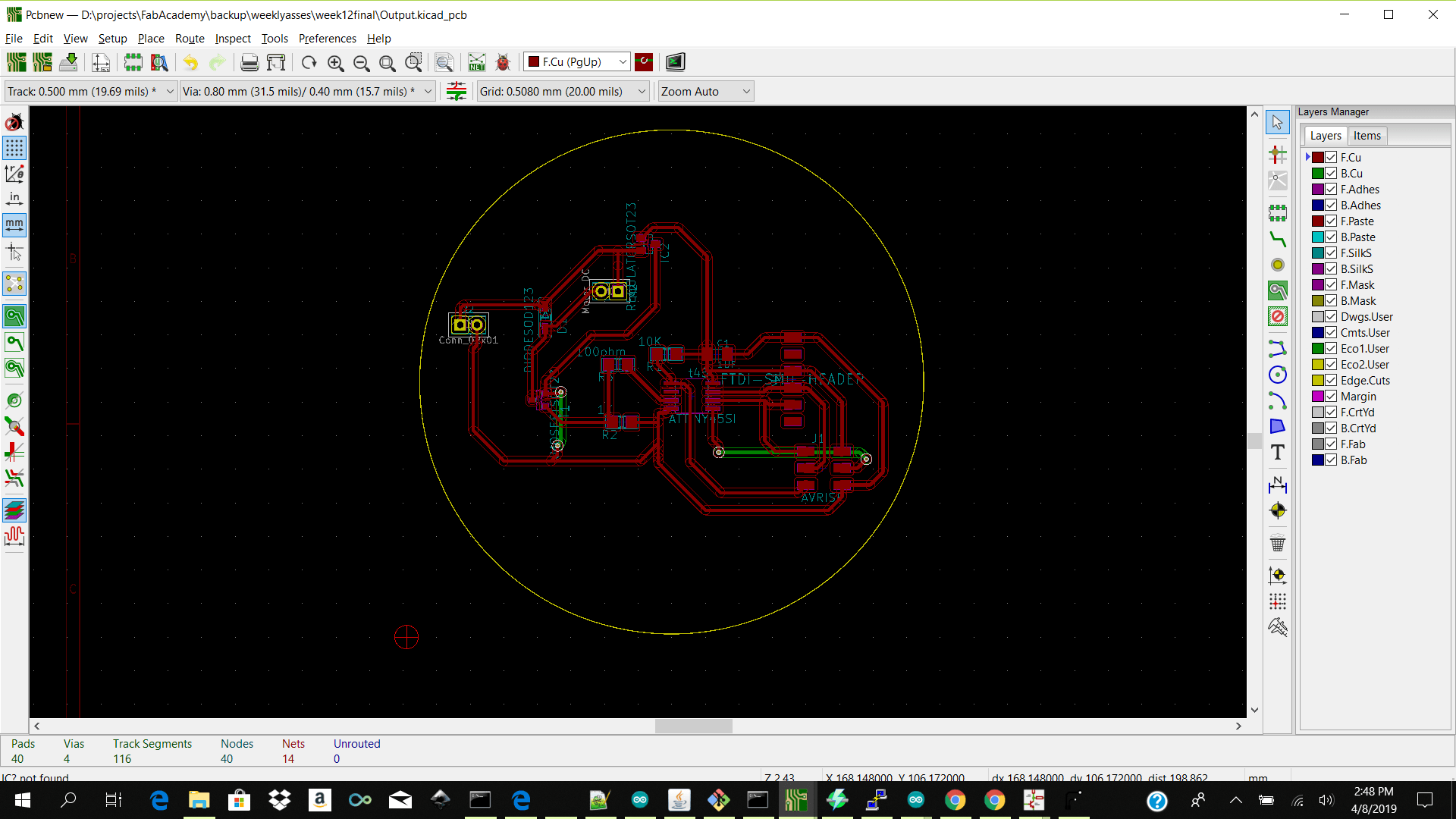
 I finally got the hang of routing my board so it was not that difficult the second time around.The only thing which was new to my design was adding vias. I had to add two vias beacause I couldnt find a way to add them in my design with the tracks alone.
This week I did not add an edge cut because we were running out of bits and they were breaking when we were cutting the edge cuts so I decided to cut the edges manually.
I finally got the hang of routing my board so it was not that difficult the second time around.The only thing which was new to my design was adding vias. I had to add two vias beacause I couldnt find a way to add them in my design with the tracks alone.
This week I did not add an edge cut because we were running out of bits and they were breaking when we were cutting the edge cuts so I decided to cut the edges manually.
 I then determined my auxillary origin using the place the auxiliary origin icon and went ahead and plot my layers. When plotting I checked off front cut and if i wanted to get the file for making the holes in my pcb for the connector pins I needed to select generate drill file. I did not want to make the hole in my pcb so I did not select generate drill files.
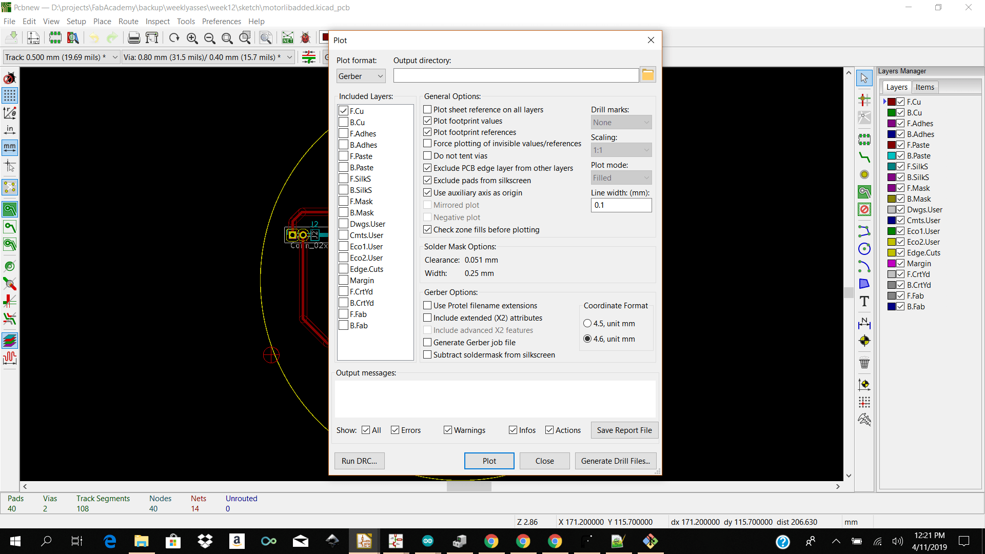 After generating my gerber files I then went ahead and open flatcam to add my parameters.
For the front cut I selected
After generating my gerber files I then went ahead and open flatcam to add my parameters.
For the front cut I selected
 I then went ahead and generated my nc files for importing into winpc nc to control the stepcraft to cut the pcb.
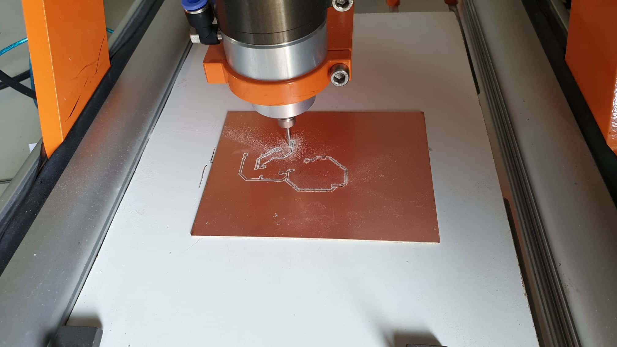
Machining
I then went and physically placed my copper plate onto the stepcraft base plate using double sided tape and imported my front cut.nc file into winpcnc. The parameters I had to keep in changer were add under Parameters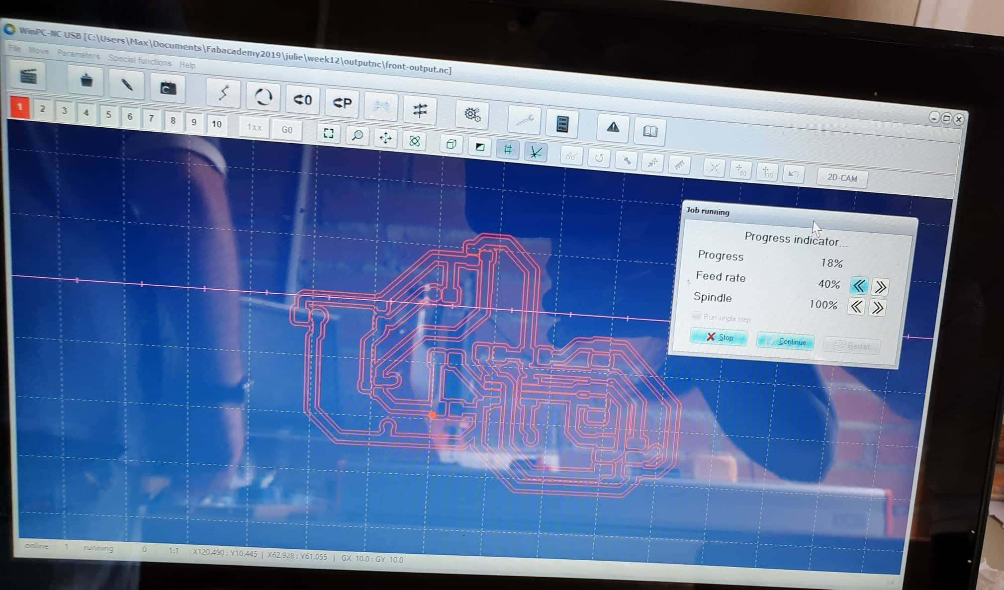
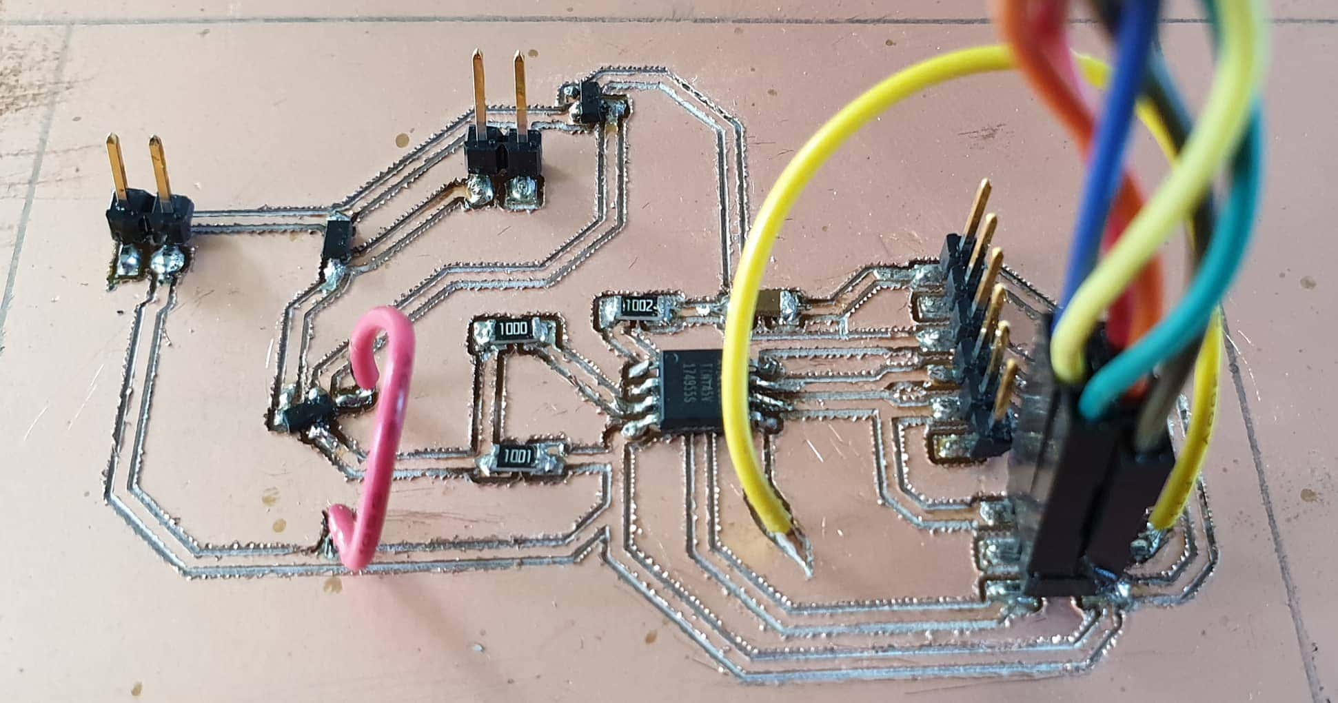
Soldering
Soldering
After I got my pcb milled I took the multimeter and checked my connections if all that needs to be connected is connected and all the does not need to be connected is not. When milling my board I realized that i went too deep on the z axis so the bit started digging my traces and leaving rough copper flakes on my board. That was also the issue because we ran out of milling bits and I was using a broken bit to mill my board for time sake. I DO NOT RECOMEND DOING THIS. I then went ahead and gathered my smd components and sensors and soldered my board.
I started off soldering my microcontroller resistors capacitor ftdi and avrisp compoents to check if my conections are good and if I can burn my bootloader.
Lessons/Problems Summary
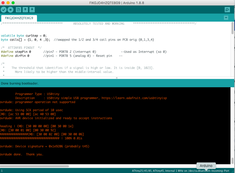
After doing my first phase soldering I realized I had a connection issue when I went back and tested my board my vias were causing my gnd connection to bridge and also the copper resdue from the rough edges were making connection where there should be. I took a knife and scrape the rough edges out abit and cut some off my traces to make sure my connections were no longer bridging. WELL THAT SOLVED THE PROBLEM. I was then able to burn the bootloader you can follow my steps below for burining the bootloader.Some things I had to keep in mind when soldering my pcb was that the diode had to be connected revered so the line needs to connect to the positve side of the motor and the regulator and mosfet gnd pin is the single one from the 3 foot.
When I powered my board from the external power supply of 8 volt my diode burnt twice and my regulator was outputing 0 volt instead of converting 8 volt to 5 volt.
When my diode burnt I realize that my resistors and capacitor and attiny was also burnt so I ended up changing all my compoents and tried reburning the bootloader and upload my code and it worked.
The next step was to test again to see if my code was running with my motor connected and my board connected via the external power supply without burning my diode or board. Well my diode was burnt again but when I took it off and run my on off code it worked fine the only issue was that the motor was not running smoothly instead there was some gitter in the sweep.
The strange thing is when I powered the board from the ftdi I got a clean sweep without gitters. I decided to stop here and conclude I got the dc to sweep but not perfectly.
Programming
After soldering my attiny 45 with my resistors and capacitor board I went ahead and programmed it. The first thing which I had to do was to connect my Output board to my fab isp and connect the fab isp to my computer and burn the bootloader using the arduino ide. I had already have the attiny core library installed from the previous week so I selected the
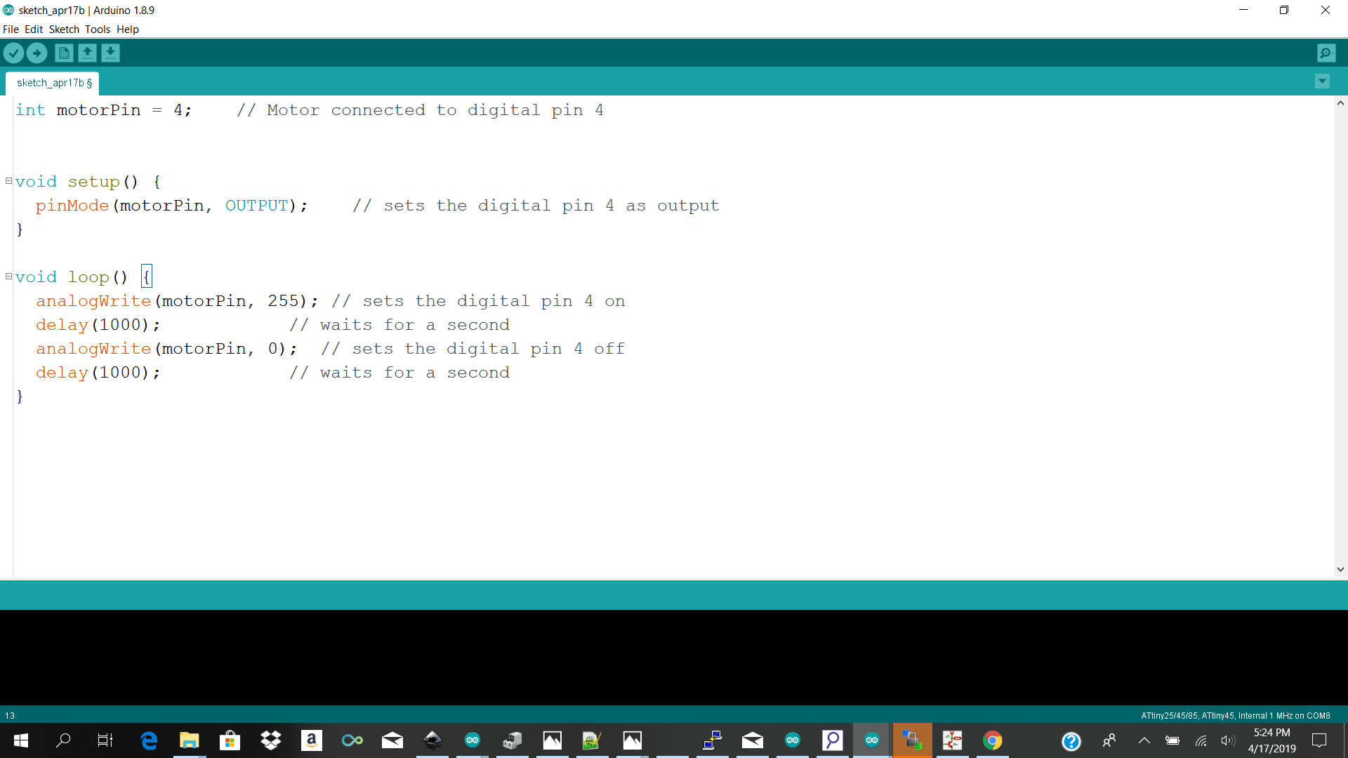
I then upladed a simple sketch to turn the motor on and off and my pin was pin 3 of the attiny 44a which maps to pin 4 of the arduino and note to define your pin as digital pin instead of analogue the analoge gave me some strange gittering.
Here is a little preview of what is happening
Download Links Here
Kicad Files Zip
Motorcontrol Zip
Contact Us
Where To Find Us
Paramaribo Suriname
Ethnalaan
50..