Assignment
group assignment:
characterize the design rules for your PCB production process
Individual assignment:
make an in-circuit programmer by milling the PCB,
program it, then optionally try other PCB processes
ATtiny45
What I did
- I have very basic knowledge about electronics. This week I have to learn from the basics. Neil introduces us different types of PCB making processes and step by step methord for soldering and desoldering. i used to solder before and I realised that I was doing the soldering wrong way.
- Learned to operate Roland Modela MDX-20 3D Milling Machine.
- Fabricated tiny ISP and programed it.
- Found ot the resolution pcb.
Roland Modela MDX-20 3D Milling Machine
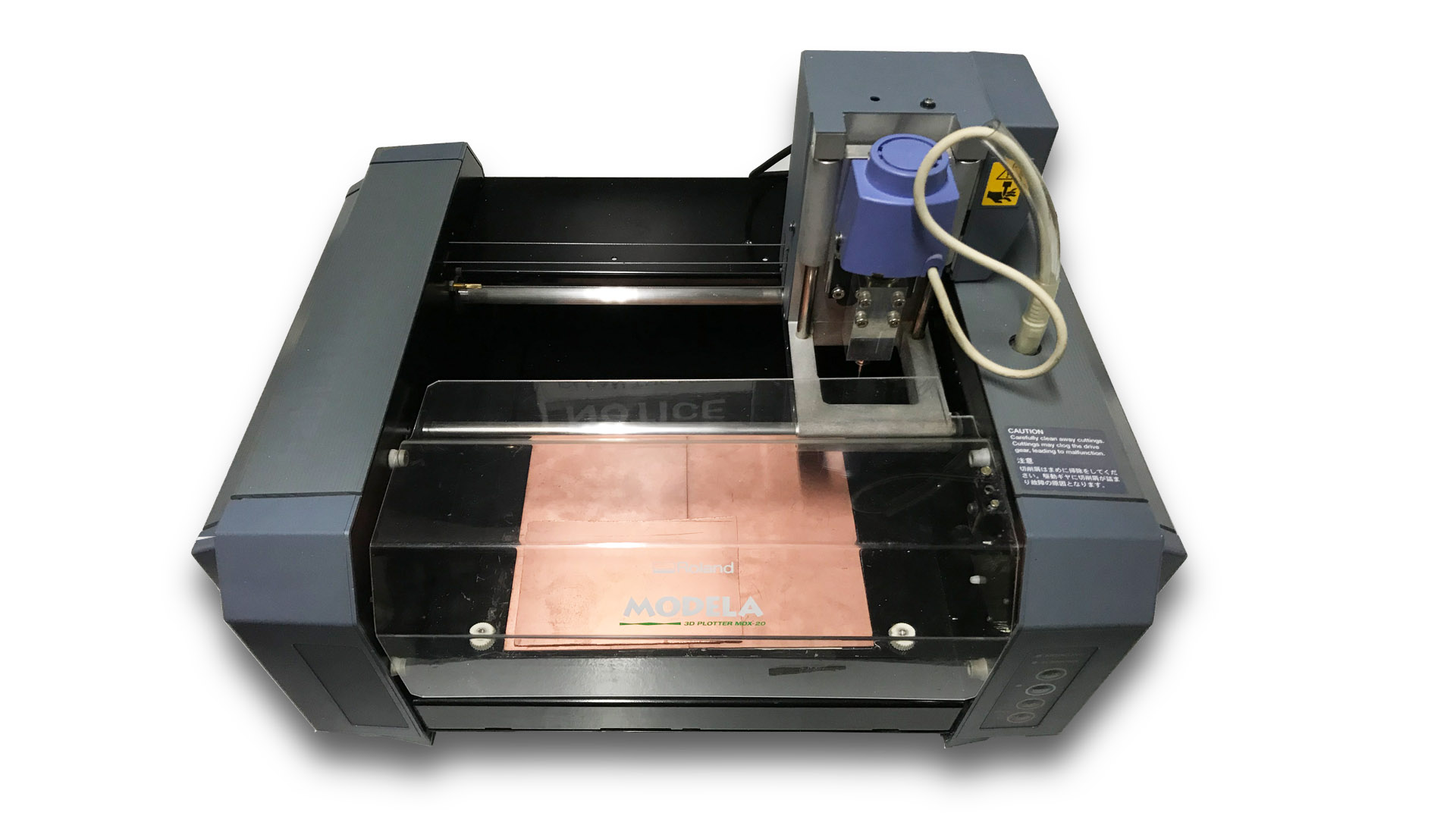
In Our Lab We have the Modella MDX 20 to machine our PCB. Modella is a Desktop milling machine that is capable of milling wood, wax, MDX,and circuit board blanks. It is compatible with most of the 2D and 3D CAD softwares. It has a small bed which moves in the Y-axis, a Tool head which moves in the X-axis and the end effector which moves in the Z-axis. It supports many milling bits and is versatile.
What is ISP(IN-SYSTEM PROGRAMMING)..?
To program a chip, we will need a special programmer which reads commands from USB to drive the SPI lines to program the chip.SPI stands for Serial Peripheral Interface and is a way for microcontrollers to communicate with each other or with the outside world. It's also called 3-wire sometimes because it uses three wires to communicate.
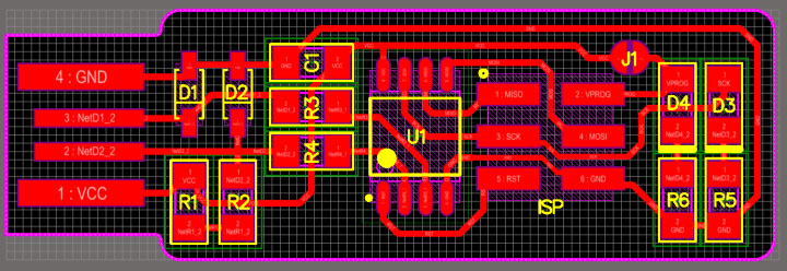
While milling pcb the black portion is the unwanted portion of copper. It will leave the traces where the components to be soldered. The 'Fab module' will remove black portion from the plate.

The outer cut is made using another png file of same size
Download design files Mill Cut

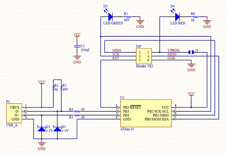
This is the schematic diagram of the circuit board.
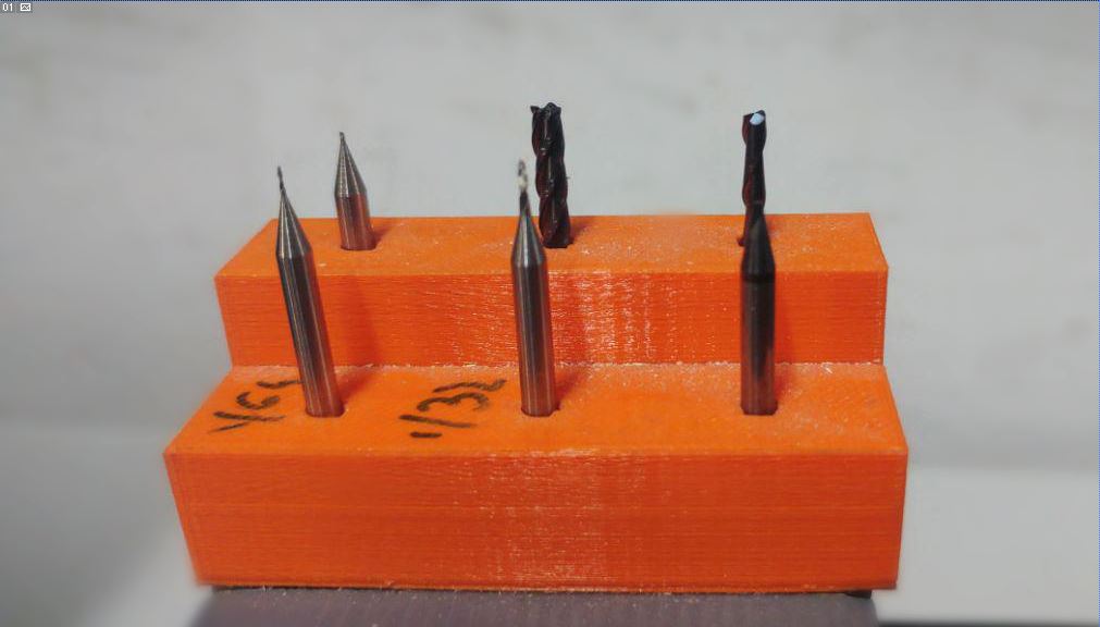
There are different type of bits used tracing and cutting, For tracing use the 1/64" bit and for cutting use 1/32" bit. These bits are very delicate, there is a chance that the bits can be broken if not handled properly.
Changing the bit
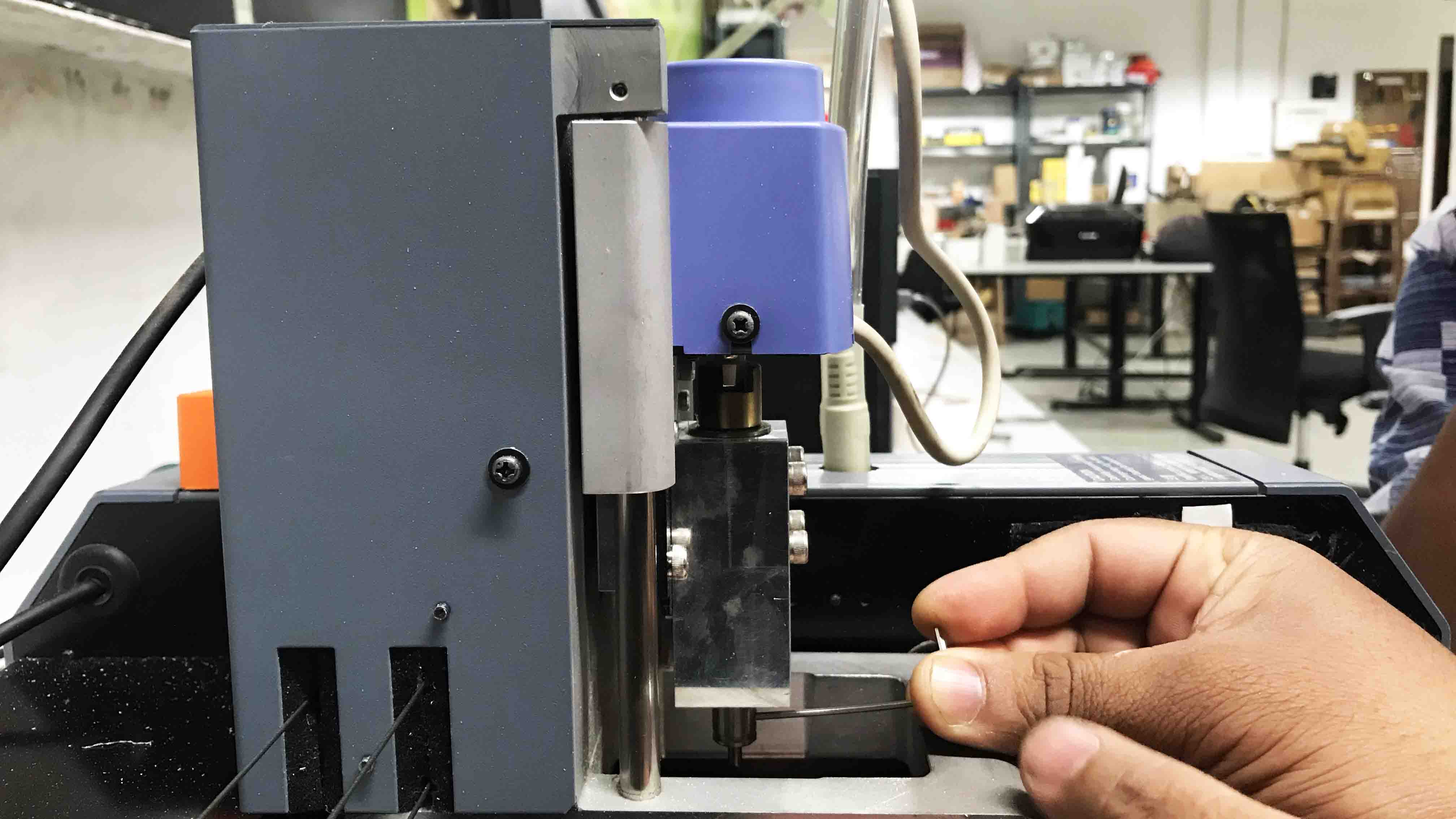
Remove the tool using ALLEN KEY. Always careful while tighting the screw since it is very delicate.
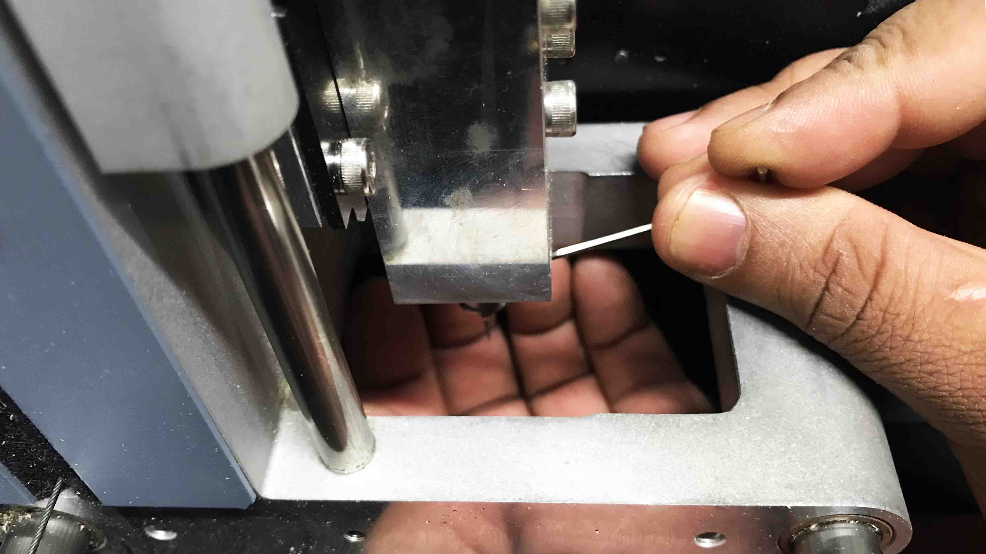
The bits are delicate, always keep hand below the tool while fixing and removing tools.
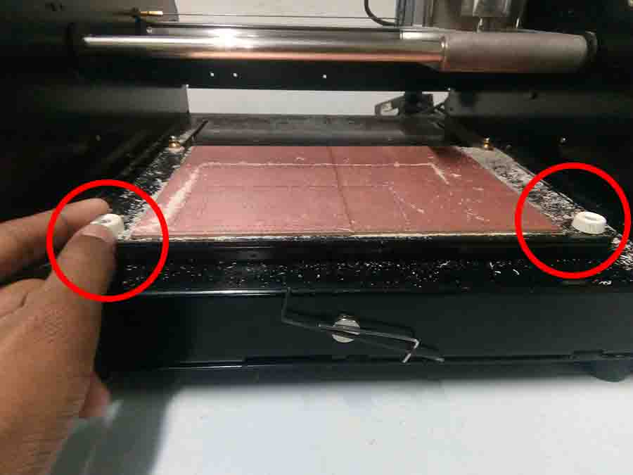
An extra layer of board is fixed on the bed as sacrificial layer. To change the sacrificial layer first reomve the screws which fixed base blate to the machine.
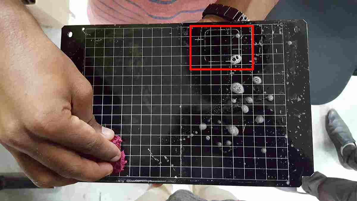
After removing the base plate remove the old sacrificial layer. Clean the base plate using Multi-purpose cleaner. In the picture you can see a mark on the metal plate made by dilling bit because someone didn't use a sacrificial layer.
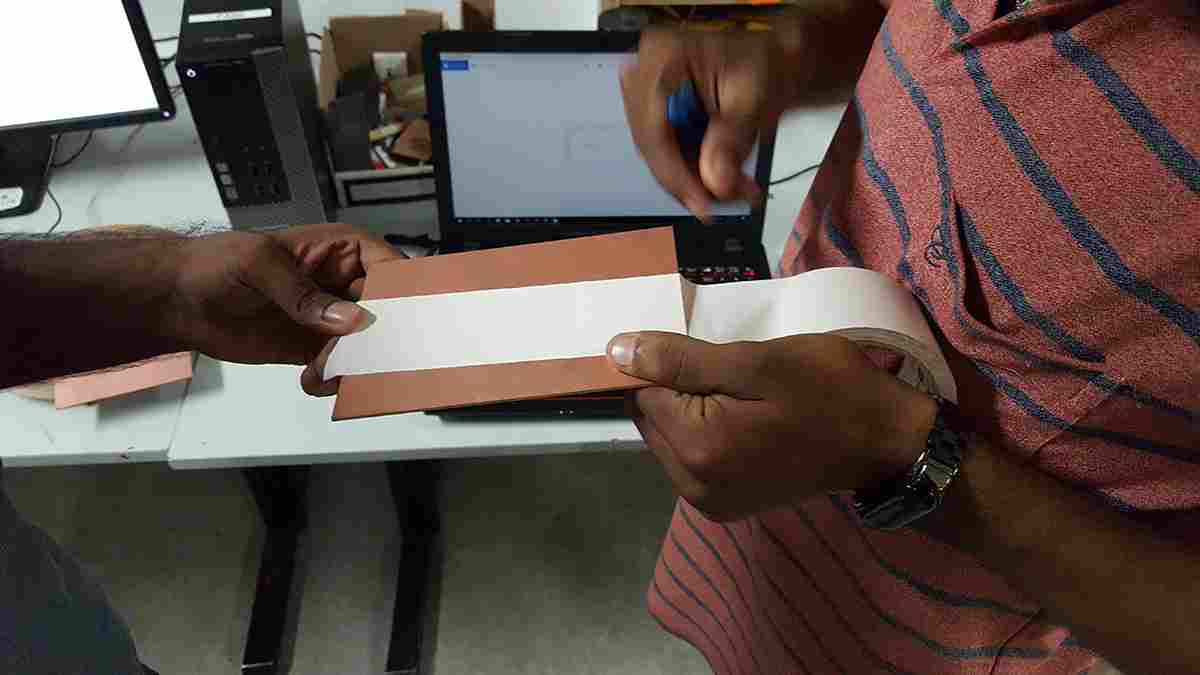
Use two side tape to fix the sacrificial layer to the bed. Make sure it is sticked perfectly flat. If the surface is not flat it will ruin the PCB.
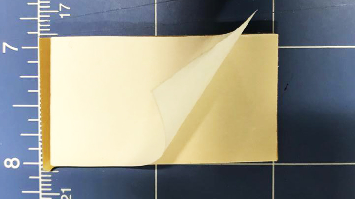
Use the two side tape for better adhesion.
Using Fab modules for milling
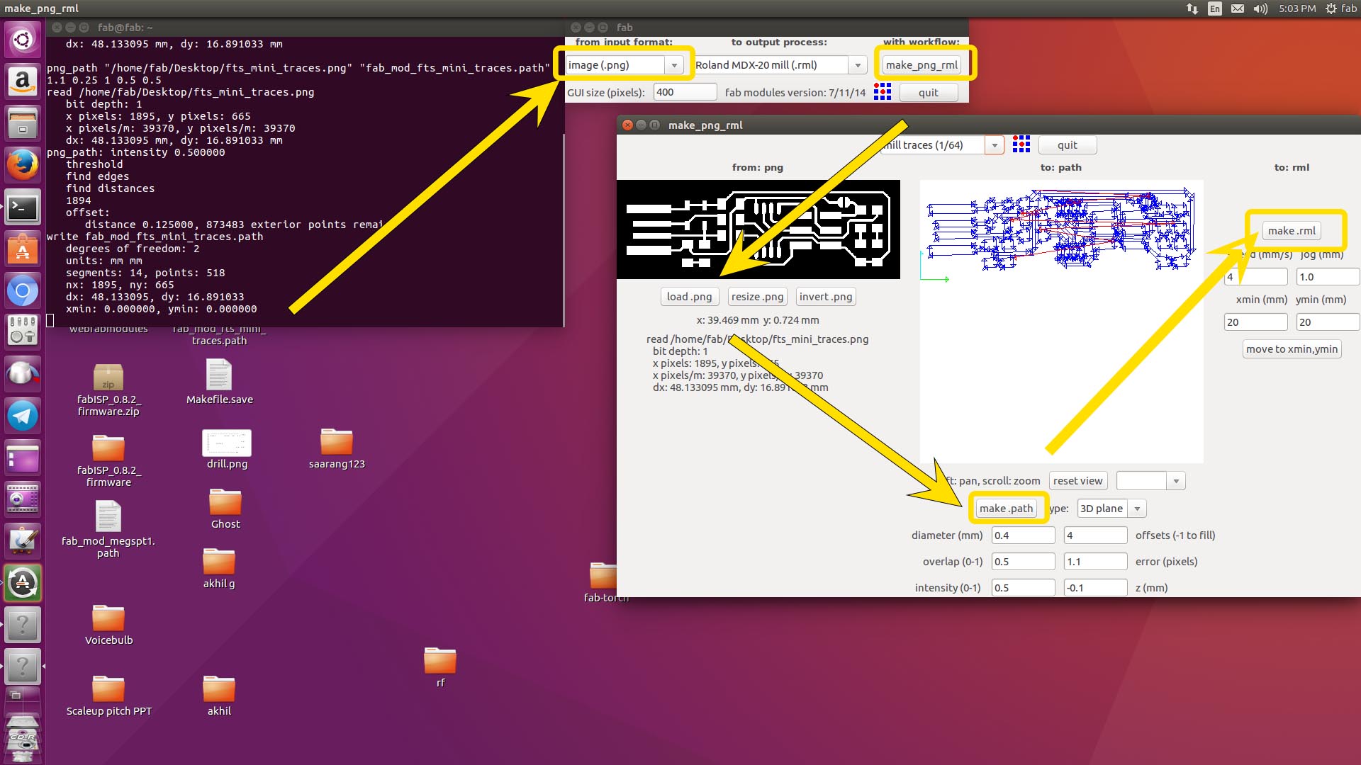
Launch the fab modules using command. Load the PNG image. Chose the printer >> Make PNG rml >> Make path >> Make rml
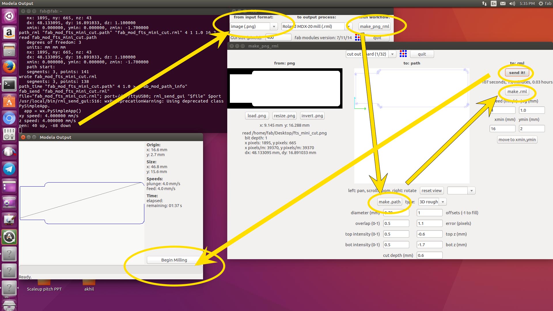
once tracing is finished, change the bit to 1/32" and mill the outer part.
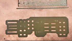
I first traced using the milling bit and ended up a failed attempt.
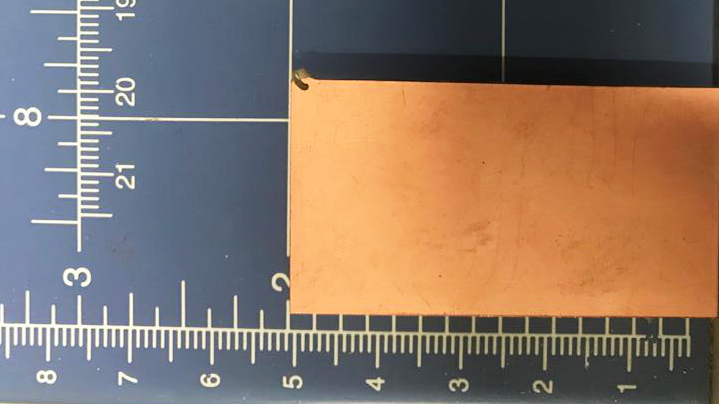
Chnaged the sheet
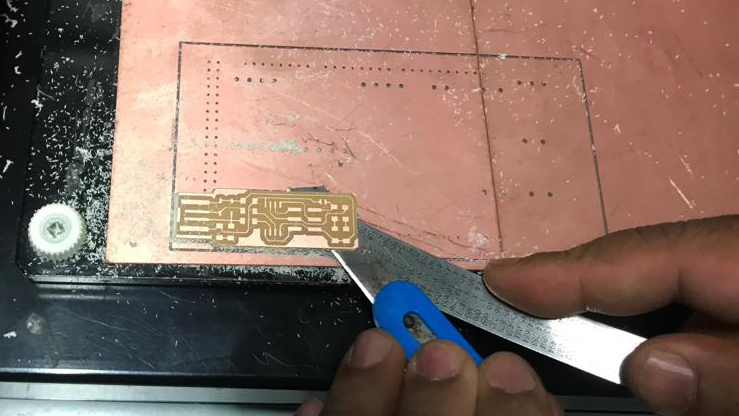
Remove the fineshed pcb carefully. I used a pen knife and steel ruler for this.
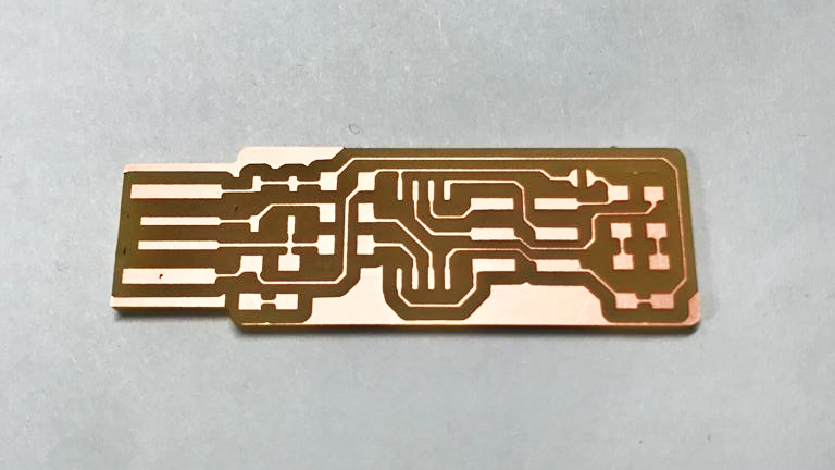
This looks like perfect circuit board.
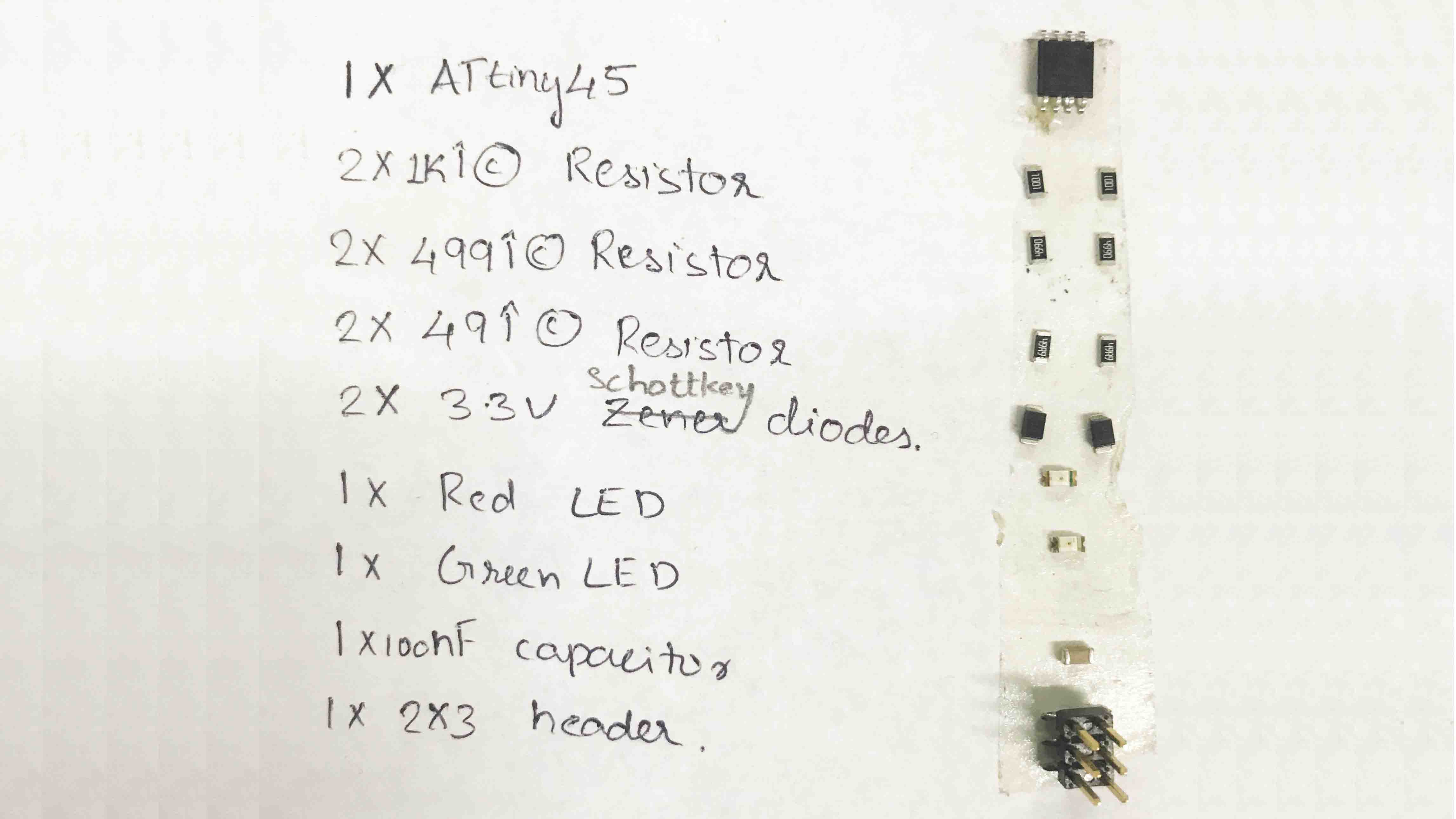
Since the components are very small in size, I wrote down their names on a paper and and used two side tape to organise them easily.
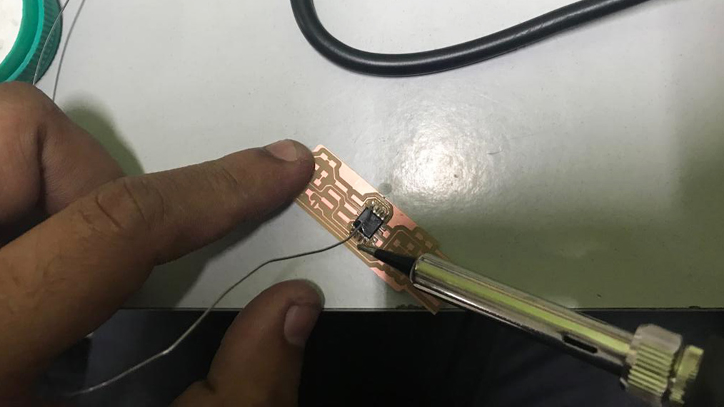
While soldering, always start from center of the pcb. while soldering IC start from any corner leg and next do the diagonally opposite leg.
ATTINY 45
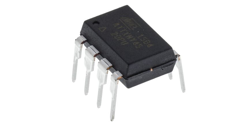
Image Source
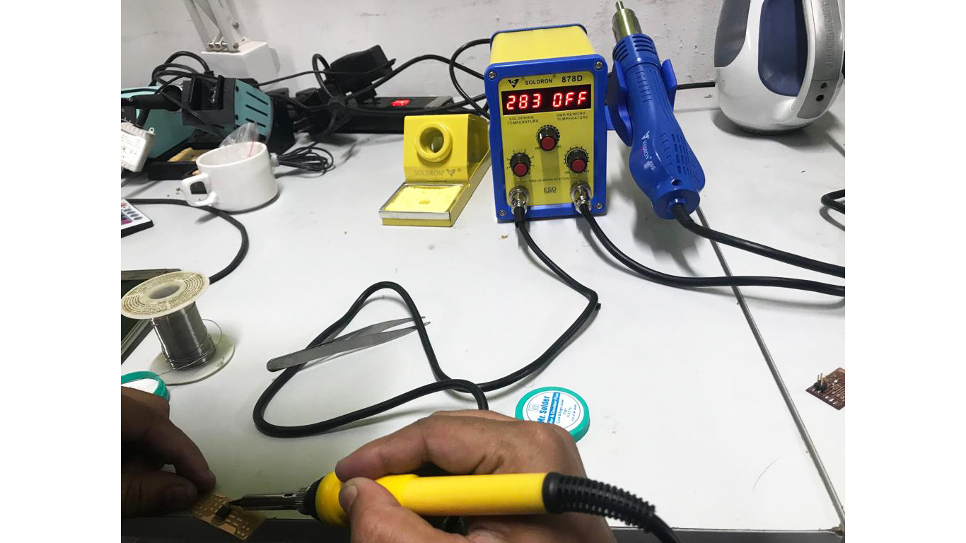
Soldering in progress.
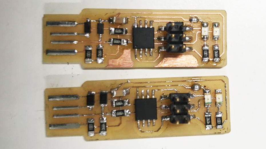
My fist board didnt work because there where a lot of cold joints. I made one more board.
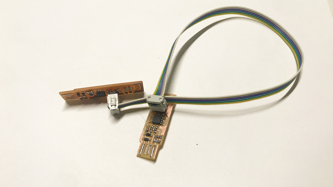
Programing ISP
I need to upload the program code for the fabISP, using Linux. First installed avr-gcc tool-chain, type this command on terminal to install tool-chian sudo
sudo apt-get install avrdude gcc-avr avr-libc make
After Installtion, unzip the downloaded firmware folder and launch terminal there.

Now we can see the files, next open the Makefile for ensuring it's configured for the ATTiny. I used nano to open the file. To launch nano typt nano Makefilein terminal.
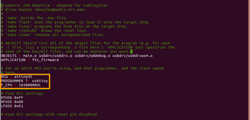
Open terminal, go to firmware path & make

Now we can see some new files, that is automatically genarated by make file script.Connect the old ISP and connect to new ISP.
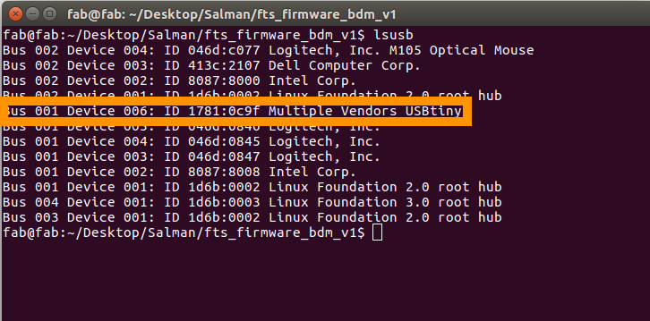
and check the new ISP was detected in Computer by Typing lsusb
Now ready for flashing. Type make flash
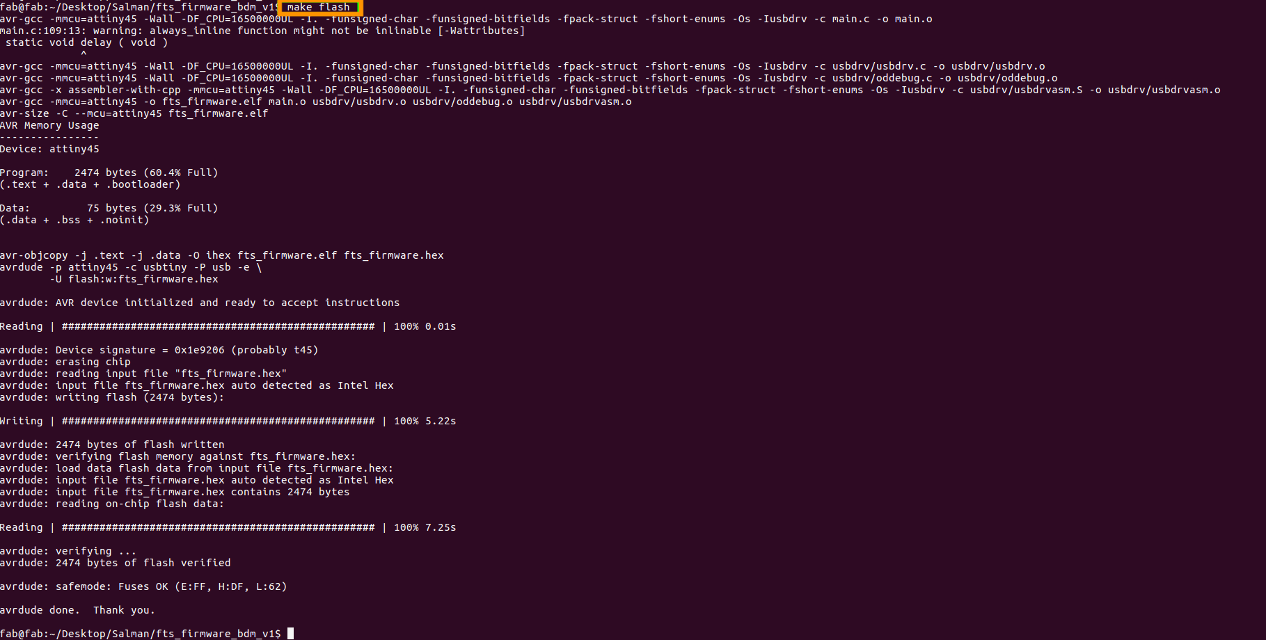
Now we have successfully flased,
to activate the fuse in order to act our ISP as a progarmmer. type Make fuse
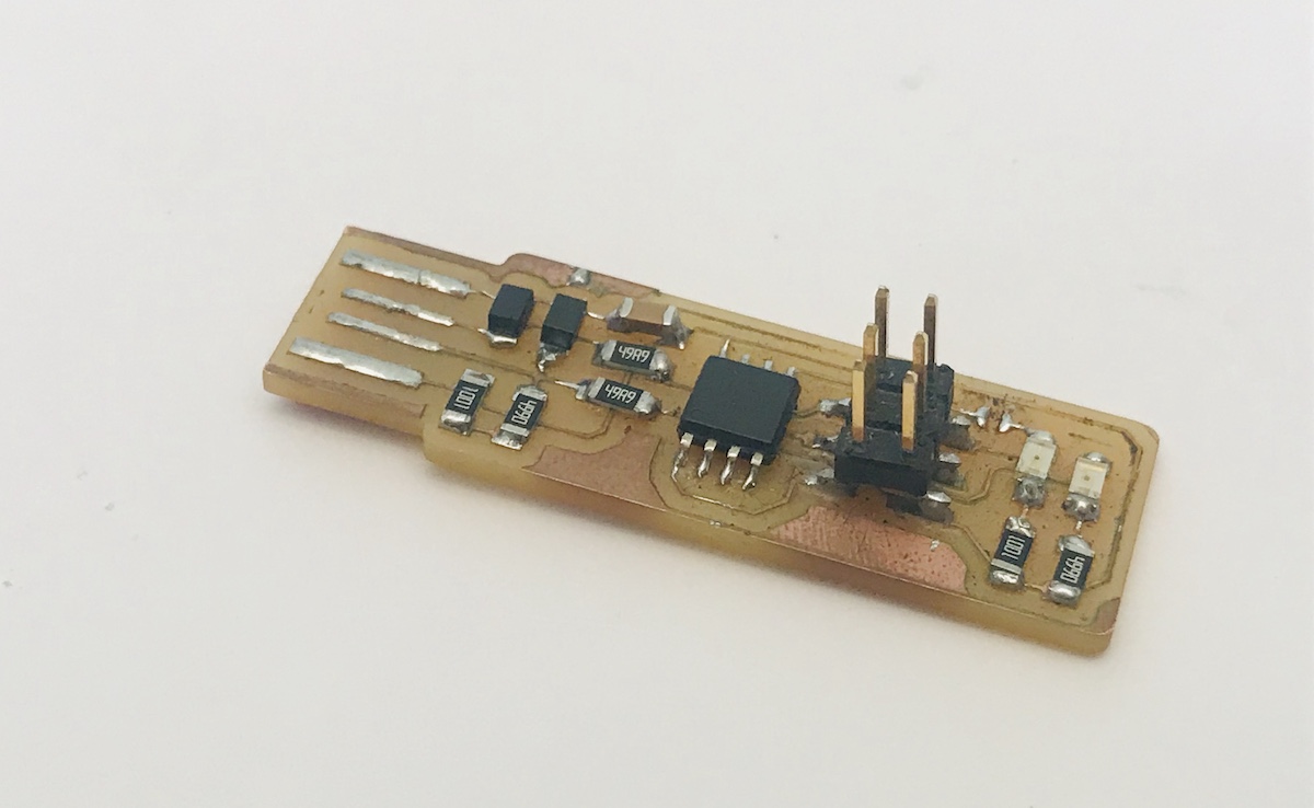
Hero shot
Group assignment
This Week we need characterize the specifications of our PCB production process we exaplined all procedure on the PCB Production section so next one is to find-out how much resolution of 1/64 and 1/100 bit can mill and find out the difference.
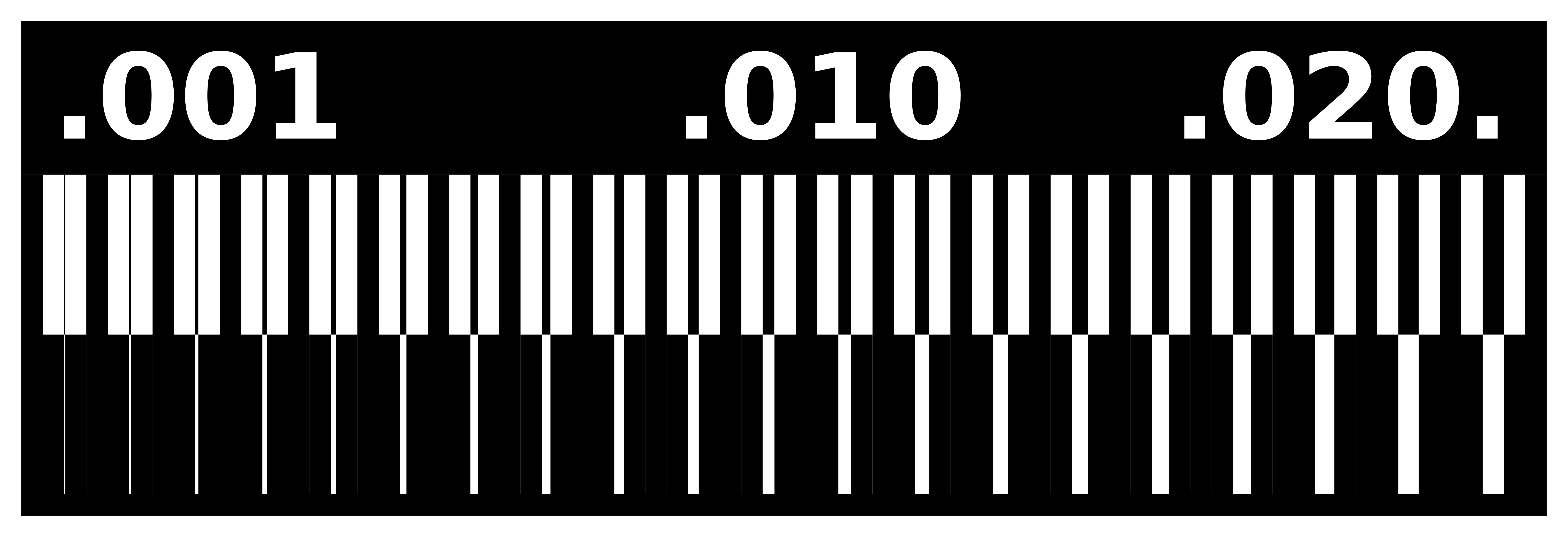
This is our test pad , so let's mill it.first i tried with 1/64 bit.
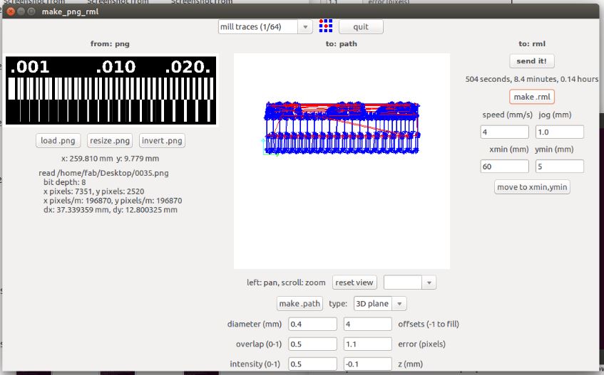
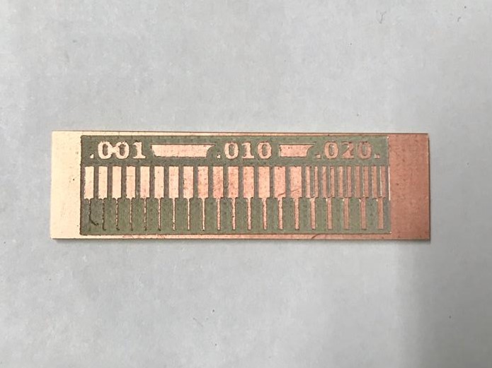
Here some copper part is not milled correctly, because I used offset as 4.
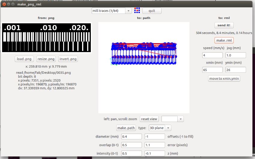
Now changed offset to -1, check the path section now it's filled completed.
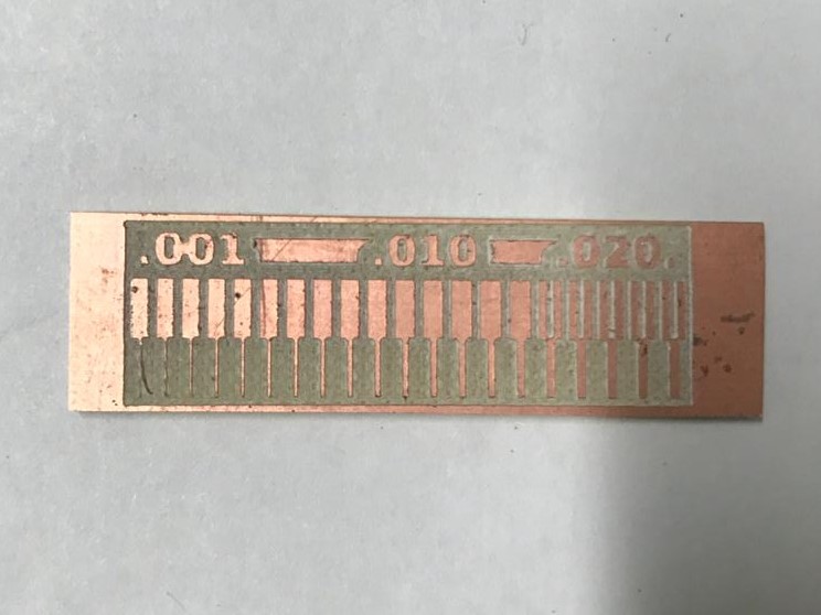
Now we got perfect one, there is no extra copper in this board , we can clearly see 1/64 only milled 0.20, and all other it's just passed. So , next I tried with 1/32.
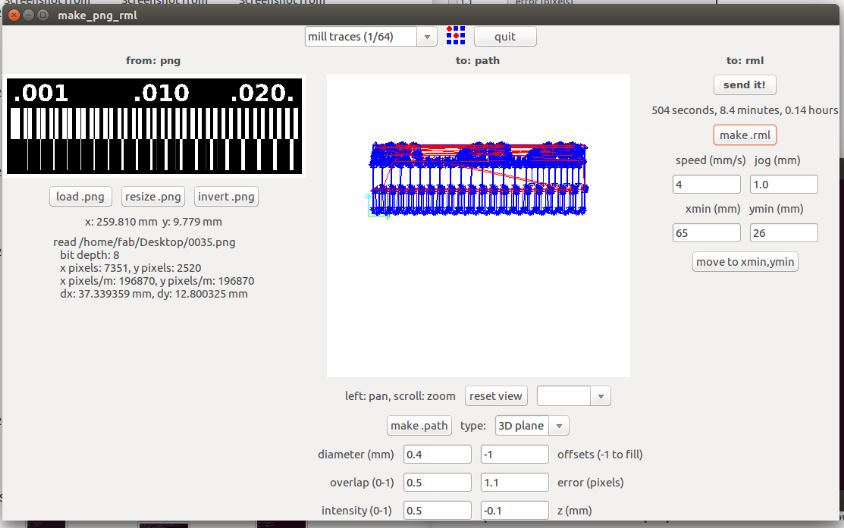
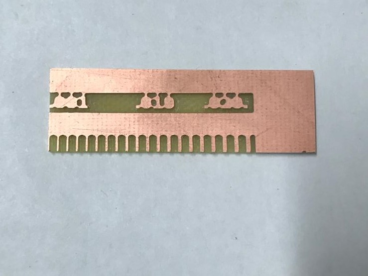
We can clearly see ,all this messed up with 1/32. This image shows cleary the milling resolution of 1/64 and 1/32 bit.