Electronics Production
In this week's Assignments we had to produce one of the given in software Programmers (ISP) and programm it so it can be used as such.
Therefore the first step is to decide on which ISP i want to build. Since all the other students chose attiny44 based boards, I decided to make a attiny45 based one. The exact board I chose is made by "Brian" and you can find it here.
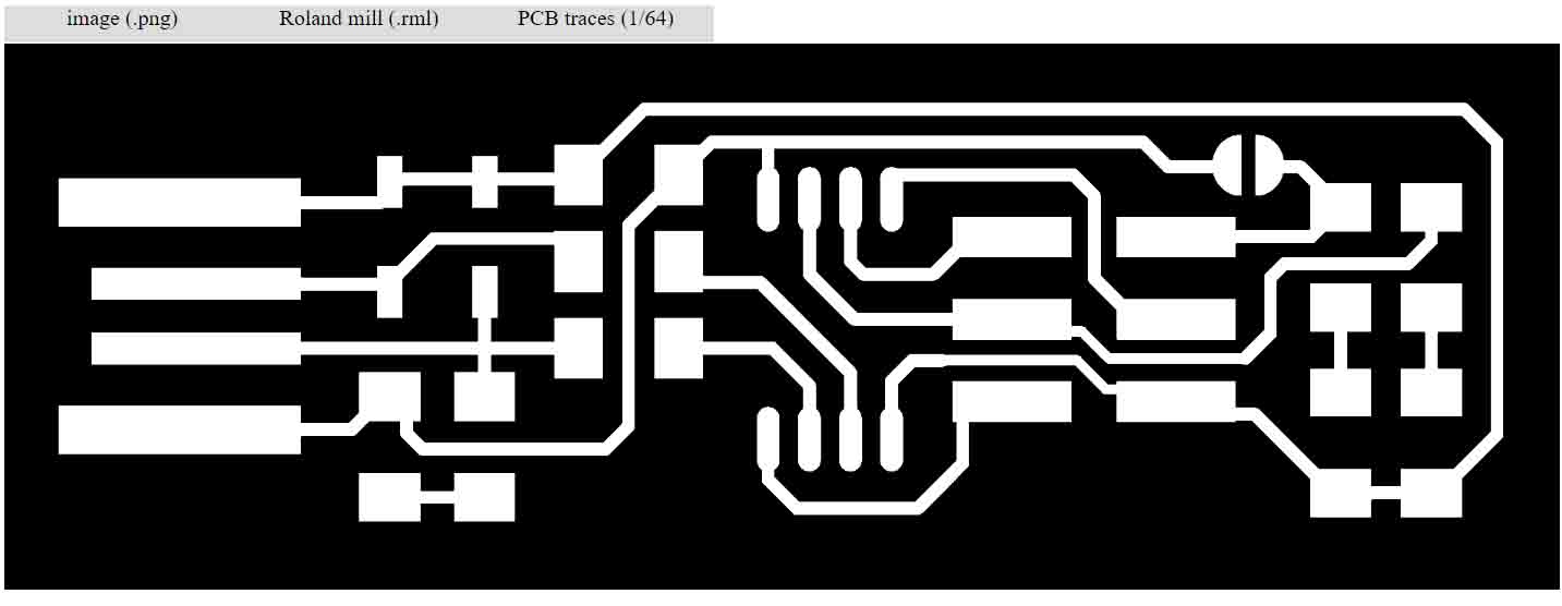
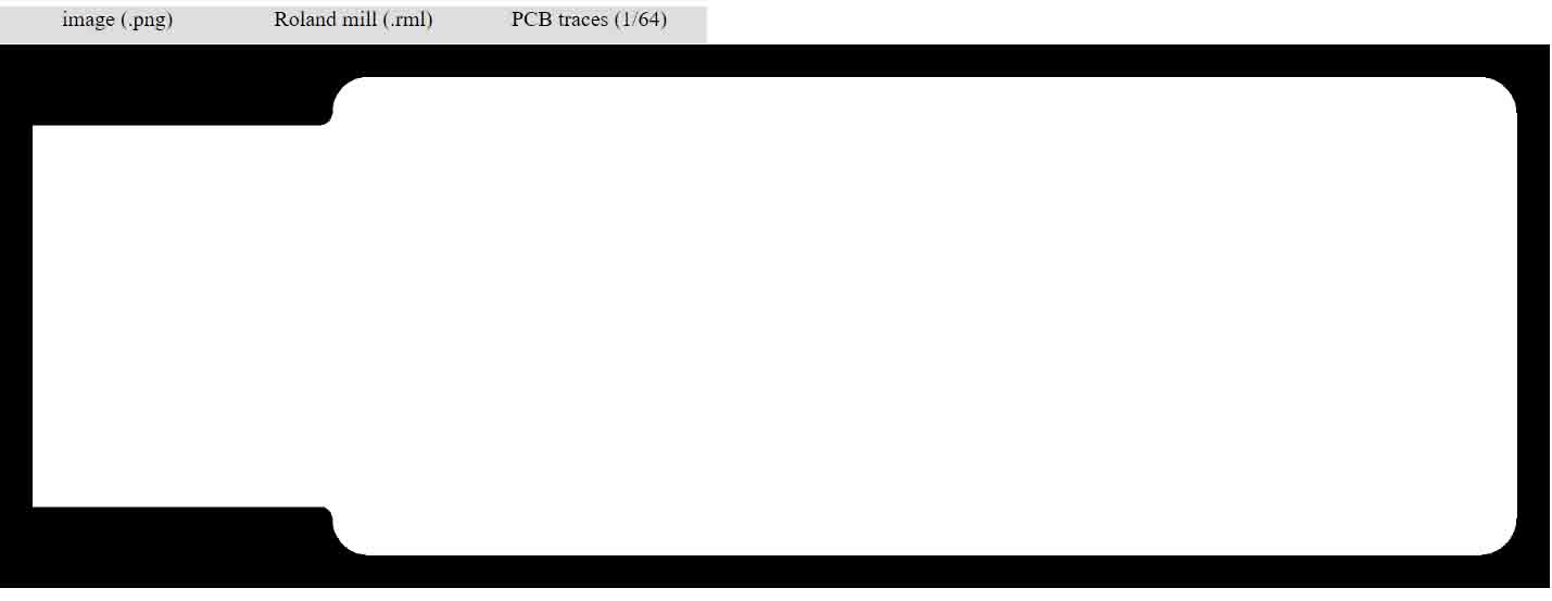
But first thing is first, after downloading the "traces" and "cut" files from the documentation, I imported them straight into the fabmodules web application, to generate g-code from them.
In the case of the traces I chose the Roland Mill file format, which is .rml and a trace width of 1/64 as the import parameters.
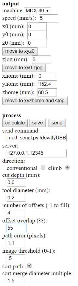
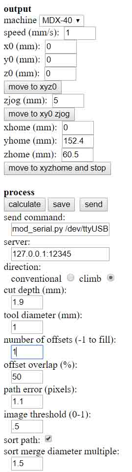
I then changed the settings as described in the following picture. Note that the depth needs to be set to 0, because we will set that up on the machine itself.
The settings that matter are speed: 5, tool diameter: 0.2, number of offsets: 4, offset overlap: 55%.
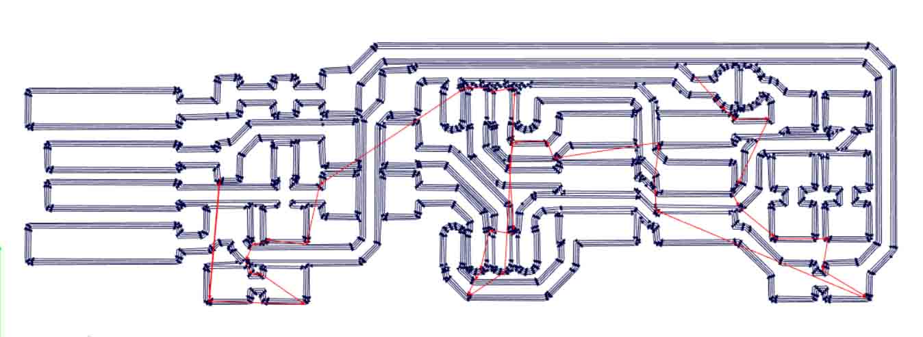
After clicking "calculate" I got this result from it, but I wasn't satisfied and wanted to know what the same board with -1 offsets (which fills non trace areas) would look like.
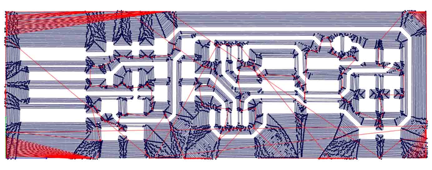
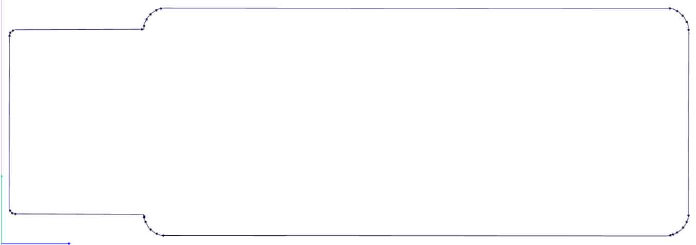
This is the second result with the offsets set to -1, as you can see it will take quite a lot longer, but that is not a problem. I then saved the generated file by clicking the "save" button.
Now I set up the g-code for the cut file. The main differences are the reduced speed (there is much more material being removed, which means the feedspeed must be lower to pervent damage), fixed depth (that of the PCBs we use) and only 1 offset (because we obviously only want to cut once around our board).
For cutting te outside, the most important settings are: speed: 1, cut depth: 1.9 (the thickness of our stock), tool diameter: 1, number of offsets: 1, offset overlap: 50%.
This then resulted in the following outcome, which was also saved.
The best way I found to mill a board and get the depth right is to first manually set it using a multimeter in continuity mode (one probe on the illing bit and the other one on the PCB, if the bit touches the PCB the multimeter beeps, so we know the depth is right) and then moving the bit up a few mills so it doesn't touch the board anymore.
That way I will have to reset the position of the cut and change the depth a couple of times, but the cut will be the best it can get.
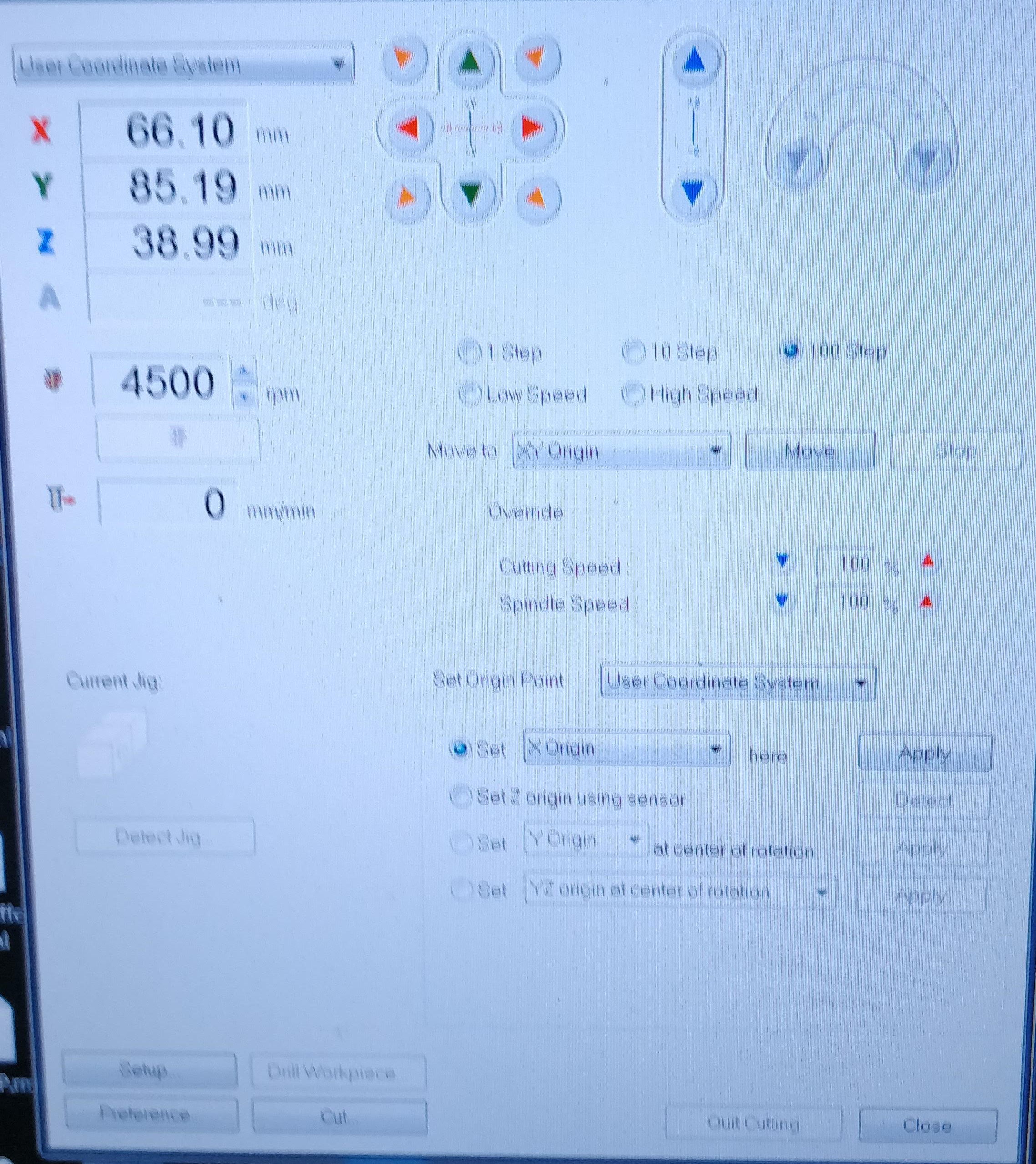
For reference, for setting the home position of the mill you have to navigate it using the above "Vpanel". You change the X and Y-value by clicking the green and red arrows. The Z-value can be changed by clicking the blue arrows. You can change the step size by selecting either 1 step, 10 step, 100 step, low speed and high speed.
After that, once you are happy with your home position you can set it as the origin.
Then you can click on "cut" and select the gcode you want the machine to use.
As I have done that noumerous times it was pretty easy for me. I set my soldering Iron to a temperature of 350°C cleaned the tip and applied a tiny bit of solder to it.
I decided to start by soldering the attiny45, so I applied a little blob of solder to one of its pads, as you can see.
.jpg)
Then I grabbed the chip with a pair of tweezers, pressed it down in the right direction (there is a little dot in one of its corners which needs to be lined up with the schematic) and heated the pretinned pad. This then tacks the chip in place and it is very easy to solder the rest of the pins to their corresponding pads, because there is no need to hold the chip in place.
.jpg)
After soldering the rest of the chip's pins, I decided to pretin one of all of the other component's pads.
this would then allow me to work much quicker as I just had to grab a component, place it on the pretinned pad and heat it, just like the attiny45.
.jpg)
I started by soldering the two smd leds. As they are diodes their orientation matters, they always have a green stripe on the side (bottom in the picture) and that is where ground needs to be connected to.
I also soldered the capacitor, which is used to stabilize the incoming power. Capacitors don't have an orientation, so you can install them however you please.
.jpg)
Then I soldered all of the resistors to the board, those also do not have a orientation.
.jpg)
Now we come to the "zener diodes" which are also called "voltage clippers" because that is exactly what they do.
In this case the diodes are 3.3V so any Voltage that is bigger than that will get clipped to 3.3V and eccess energy is dissipated as heat. This also works the other way around, so if the Voltage is lower that 3.3V it gets bumped up, but because of conservation of energy the current goes down significantly.
As they are diodes, they also have a orientation, which is indicated by a faint white line on one of its sides.
.jpg)
Here They are soldered on and the line is much easier to see.
.jpg)
Now I had to solder the 3x2 pinheader to the big pads on the board. To do that I utilized the same technique that I used to solder the chip just with way more solder, because these headers must withstand a lot of mechanical stress from wires being plugged in and pulled out of them.
.jpg)
As you can see here, I then soldered the rest if the pins to the board.
.jpg)
The last step was to bridge the jumper (which is not shown in the picture, but very straight forward) and add lots of solder to the usb connector, to add height so it has enougth hold when you plug it in.
.jpg)
Since I use a windows based laptop, I decided to program it in a Linux virtual machine I had already installed.
This is beacause I tried with windows before, but couldn't get it to work properly. I followed the steps described here. But still as I tried to flash my chip windows wouldn't let me because of permission reasons. Which did not make any sense and was a real hassle to debug, therefore I switched to the VM.
The software I used to create the VM is called virtualbox and can be downloaded here.
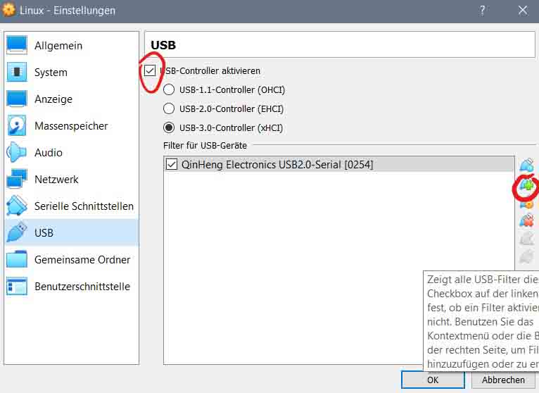
You will need to forward the Serial Port from the host to the VM. To do that you first need to activate the USB-controller in the usb settings, then you need to select the correct device in the list that pops up, when you press the little plus button on the right.
Then just start your VM and everything should work fine, first you will need to install the AVR toolchain, which is done by typing the following command into the terminal (crtl + alt + t to open the terminal):

After that we download the firmware from the same site we got the cut and traces file from.
Then we unzip it, by cd'ing into the folder where it is located and typing:

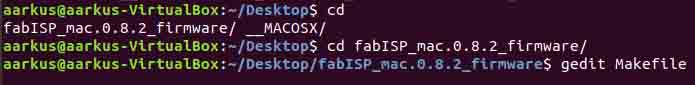
After that cd into the extracted folder and open the Makefile in any texteditor.
In my case I used gedit, the full command is:
Then the Makefile has to be edited like shown below (all of the orange highlighted lines are changed), this let's you choose the port by editing the port variable at the top. Also the programmer has to be changed to stk500v1, if you are using the arduino as ISP for programming.
Then we need to set the fuses of the chip, by typing the command:
After that we are almost done, and we can try to plug the ISP into the USB port of an USB-hub. To check if it is working we open the device manager and look if the ISP gets recognized as "USBtinySPI" under "other devices". If that is the case we can assume everything worked and we can move on to the very last step.

The very last step to complete the programming of the chip is burning the reset fuse. This is done by typing the following in the console:
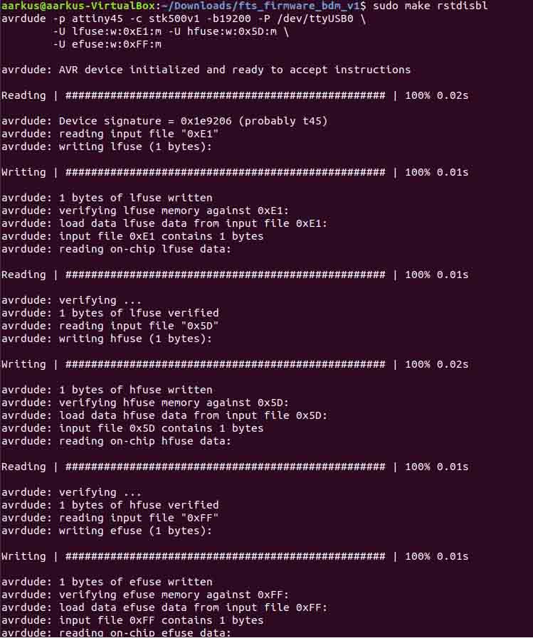
Now the ISP is finished and the only step left to do is disconnecting the jumper!
.jpg)
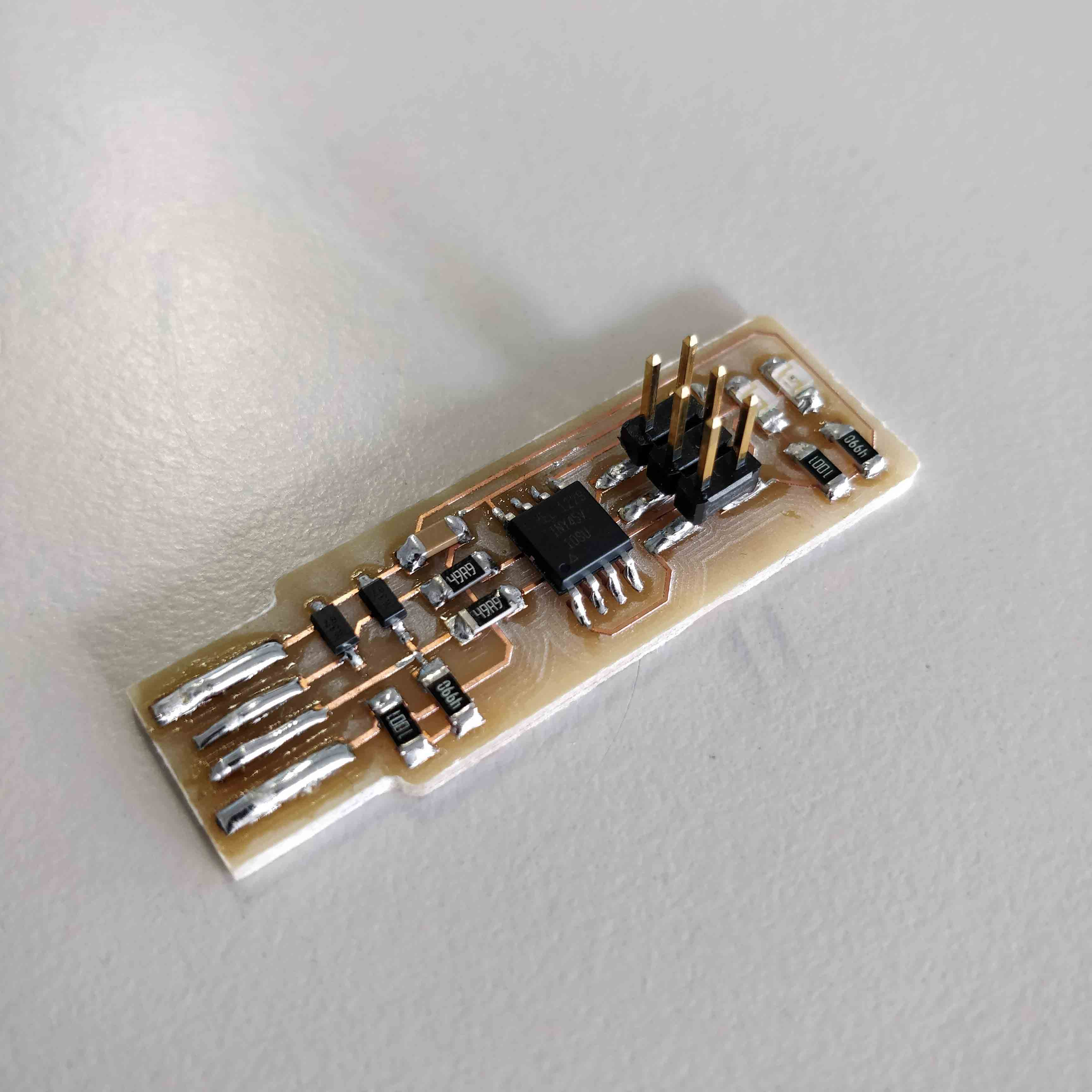
Here is the picture of my Final outcome!
Download all the used files!
Therefore the first step is to decide on which ISP i want to build. Since all the other students chose attiny44 based boards, I decided to make a attiny45 based one. The exact board I chose is made by "Brian" and you can find it here.
But first thing is first, after downloading the "traces" and "cut" files from the documentation, I imported them straight into the fabmodules web application, to generate g-code from them.
In the case of the traces I chose the Roland Mill file format, which is .rml and a trace width of 1/64 as the import parameters.
Milling
I then changed the settings as described in the following picture. Note that the depth needs to be set to 0, because we will set that up on the machine itself.
The settings that matter are speed: 5, tool diameter: 0.2, number of offsets: 4, offset overlap: 55%.
After clicking "calculate" I got this result from it, but I wasn't satisfied and wanted to know what the same board with -1 offsets (which fills non trace areas) would look like.
This is the second result with the offsets set to -1, as you can see it will take quite a lot longer, but that is not a problem. I then saved the generated file by clicking the "save" button.
Now I set up the g-code for the cut file. The main differences are the reduced speed (there is much more material being removed, which means the feedspeed must be lower to pervent damage), fixed depth (that of the PCBs we use) and only 1 offset (because we obviously only want to cut once around our board).
For cutting te outside, the most important settings are: speed: 1, cut depth: 1.9 (the thickness of our stock), tool diameter: 1, number of offsets: 1, offset overlap: 50%.
This then resulted in the following outcome, which was also saved.
The best way I found to mill a board and get the depth right is to first manually set it using a multimeter in continuity mode (one probe on the illing bit and the other one on the PCB, if the bit touches the PCB the multimeter beeps, so we know the depth is right) and then moving the bit up a few mills so it doesn't touch the board anymore.
That way I will have to reset the position of the cut and change the depth a couple of times, but the cut will be the best it can get.
For reference, for setting the home position of the mill you have to navigate it using the above "Vpanel". You change the X and Y-value by clicking the green and red arrows. The Z-value can be changed by clicking the blue arrows. You can change the step size by selecting either 1 step, 10 step, 100 step, low speed and high speed.
After that, once you are happy with your home position you can set it as the origin.
Then you can click on "cut" and select the gcode you want the machine to use.
Soldering
After the milling was done, it was finally time to solder the components to the (not yet) ISP.As I have done that noumerous times it was pretty easy for me. I set my soldering Iron to a temperature of 350°C cleaned the tip and applied a tiny bit of solder to it.
I decided to start by soldering the attiny45, so I applied a little blob of solder to one of its pads, as you can see.
Then I grabbed the chip with a pair of tweezers, pressed it down in the right direction (there is a little dot in one of its corners which needs to be lined up with the schematic) and heated the pretinned pad. This then tacks the chip in place and it is very easy to solder the rest of the pins to their corresponding pads, because there is no need to hold the chip in place.
After soldering the rest of the chip's pins, I decided to pretin one of all of the other component's pads.
this would then allow me to work much quicker as I just had to grab a component, place it on the pretinned pad and heat it, just like the attiny45.
I started by soldering the two smd leds. As they are diodes their orientation matters, they always have a green stripe on the side (bottom in the picture) and that is where ground needs to be connected to.
I also soldered the capacitor, which is used to stabilize the incoming power. Capacitors don't have an orientation, so you can install them however you please.
Then I soldered all of the resistors to the board, those also do not have a orientation.
Now we come to the "zener diodes" which are also called "voltage clippers" because that is exactly what they do.
In this case the diodes are 3.3V so any Voltage that is bigger than that will get clipped to 3.3V and eccess energy is dissipated as heat. This also works the other way around, so if the Voltage is lower that 3.3V it gets bumped up, but because of conservation of energy the current goes down significantly.
As they are diodes, they also have a orientation, which is indicated by a faint white line on one of its sides.
Here They are soldered on and the line is much easier to see.
Now I had to solder the 3x2 pinheader to the big pads on the board. To do that I utilized the same technique that I used to solder the chip just with way more solder, because these headers must withstand a lot of mechanical stress from wires being plugged in and pulled out of them.
As you can see here, I then soldered the rest if the pins to the board.
The last step was to bridge the jumper (which is not shown in the picture, but very straight forward) and add lots of solder to the usb connector, to add height so it has enougth hold when you plug it in.
Programming
Now that the board is finished, I can go on to programm it!Since I use a windows based laptop, I decided to program it in a Linux virtual machine I had already installed.
This is beacause I tried with windows before, but couldn't get it to work properly. I followed the steps described here. But still as I tried to flash my chip windows wouldn't let me because of permission reasons. Which did not make any sense and was a real hassle to debug, therefore I switched to the VM.
The software I used to create the VM is called virtualbox and can be downloaded here.
You will need to forward the Serial Port from the host to the VM. To do that you first need to activate the USB-controller in the usb settings, then you need to select the correct device in the list that pops up, when you press the little plus button on the right.
Then just start your VM and everything should work fine, first you will need to install the AVR toolchain, which is done by typing the following command into the terminal (crtl + alt + t to open the terminal):
sudo apt-get install avrdude gcc-avr avr-libc make
After that we download the firmware from the same site we got the cut and traces file from.
Then we unzip it, by cd'ing into the folder where it is located and typing:
sudo unzip firmware.zip
After that cd into the extracted folder and open the Makefile in any texteditor.
In my case I used gedit, the full command is:
sudo gedit Makefile
Then the Makefile has to be edited like shown below (all of the orange highlighted lines are changed), this let's you choose the port by editing the port variable at the top. Also the programmer has to be changed to stk500v1, if you are using the arduino as ISP for programming.
                # Generic AVR Makefile - Adapted for FabTinyStar
# Brian Mayton
#
# 'make' builds the .hex file.
# 'make flash' uses the programmer to load it onto the target chip.
# 'make fuses' programs the fuse bits on the target chip.
# 'make rstdisbl' blows the reset fuse.
# 'make clean' removes all autogenerated files.

# OBJECTS should list all of the object files for the program (e.g. for each
# .c file, list a corresponding .o file here.)  APPLICATION just specifies the
# name of the hex/elf files, and can be whatever you want.
OBJECTS = main.o usbdrv/usbdrv.o usbdrv/oddebug.o usbdrv/usbdrvasm.o
APPLICATION = fts_firmware

# Set up which MCU you're using, and what programmer, and the clock speed
# here.
MCU = attiny45
 PROGRAMMER ?= stk500v1
F_CPU = 16000000UL
port= /dev/ttyS4

# Fuse bit settings
EFUSE=0xFF
HFUSE=0xDD
LFUSE=0xE1


# Fuse bit settings with reset pin disabled
HFUSE_RSTDISBL=0x5D

# Edit these if you want to use different compilers
CC = avr-gcc
OBJCOPY = avr-objcopy
SIZE = avr-size
AVRDUDE = avrdude


# Compiler and linker flags
CFLAGS=-mmcu=$(MCU) -Wall -DF_CPU=$(F_CPU) -I. -funsigned-char \
  -funsigned-bitfields -fpack-struct -fshort-enums -Os -Iusbdrv
LDFLAGS=-mmcu=$(MCU)

all: $(APPLICATION).hex

clean:
  rm -f usbdrv/*.o
  rm -f *.hex *.elf *.o

%.hex: %.elf
  $(OBJCOPY) -j .text -j .data -O ihex $< $@

$(APPLICATION).elf: $(OBJECTS)
  $(CC) $(LDFLAGS) -o $@ $^
  $(SIZE) -C --mcu=$(MCU) $@

%.o: %.c
  $(CC) $(CFLAGS) -c $< -o $@

%.o: %.S
  $(CC) -x assembler-with-cpp $(CFLAGS) -c $< -o $@

flash: all
  $(AVRDUDE) -p $(MCU) -c $(PROGRAMMER) -b19200 -P $(port) -e \
    -U flash:w:$(APPLICATION).hex

fuses:

  $(AVRDUDE) -p $(MCU) -c $(PROGRAMMER) -b19200 -P $(port) \
    -U lfuse:w:$(LFUSE):m -U hfuse:w:$(HFUSE):m \
    -U efuse:w:$(EFUSE):m

rstdisbl:
  $(AVRDUDE) -p $(MCU) -c $(PROGRAMMER) -b19200 -P $(port) \
    -U lfuse:w:$(LFUSE):m -U hfuse:w:$(HFUSE_RSTDISBL):m \
    -U efuse:w:$(EFUSE):m

.PHONY: all clean install fuses
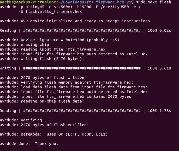
Then we need to generate the files that will be used to flash onto the chip. To do that we type the following command:
sudo make flash
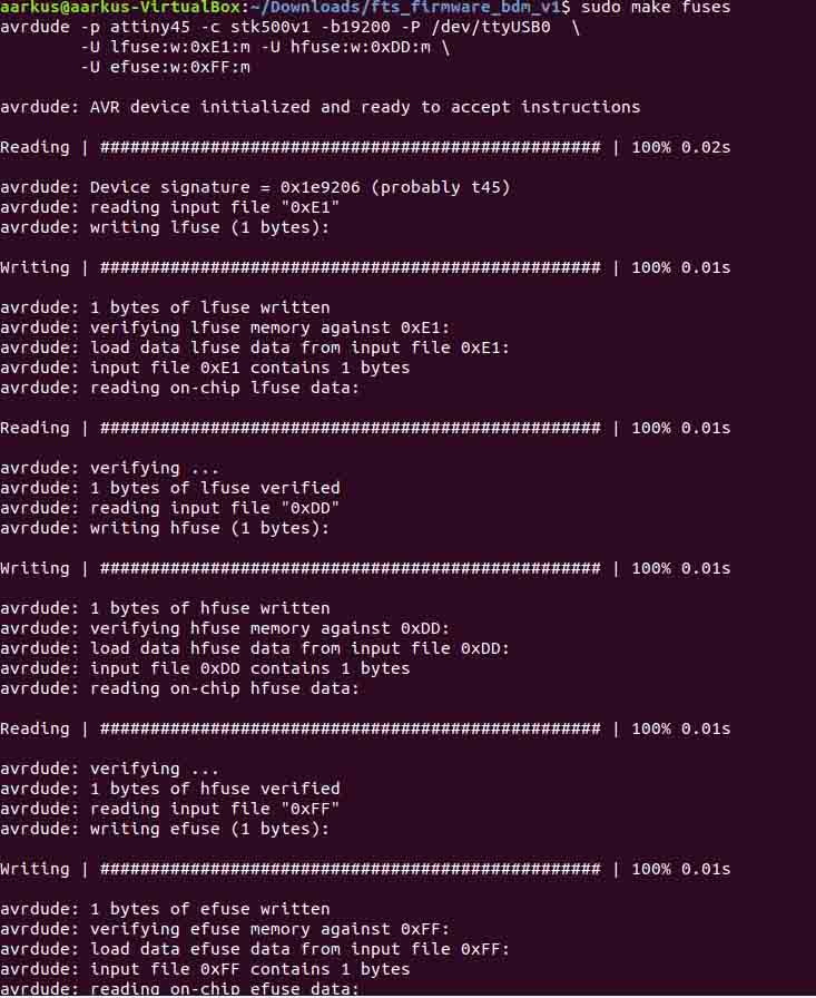
Then we need to set the fuses of the chip, by typing the command:
sudo make fuses
After that we are almost done, and we can try to plug the ISP into the USB port of an USB-hub. To check if it is working we open the device manager and look if the ISP gets recognized as "USBtinySPI" under "other devices". If that is the case we can assume everything worked and we can move on to the very last step.
The very last step to complete the programming of the chip is burning the reset fuse. This is done by typing the following in the console:
sudo make rstdisbl
Now the ISP is finished and the only step left to do is disconnecting the jumper!
Here is the picture of my Final outcome!
Download all the used files!