For this week's group assignment we had to use the test equipment in our lab to observe the operation of a microcontroller board.
Group Assignment: Electronics Design
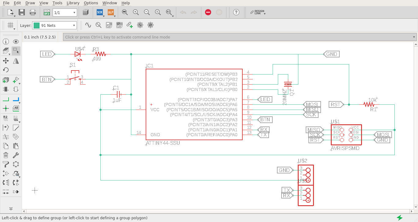
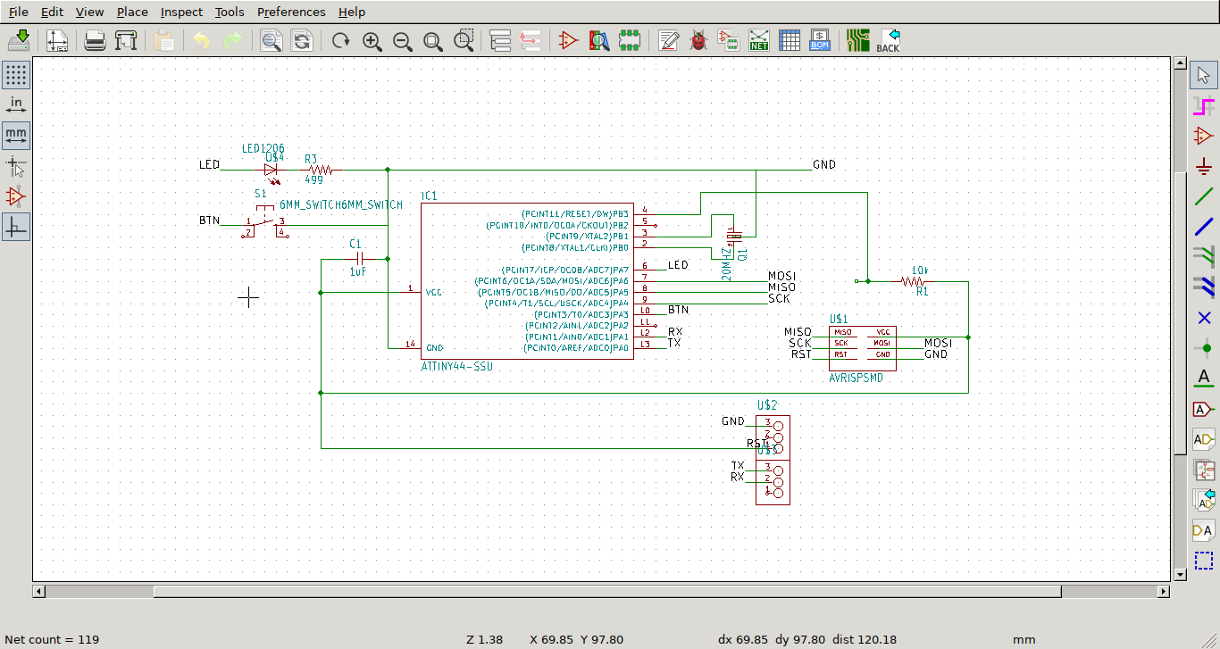
The first program I tested was Autodesk Eagle. I redrew the board using the fab.lbr component library and added both an LED with a 499 Ohm resistor to lower the current and a button. Normally one would need a pull-down or pull-up resistor to operate the button, but the ATtiny44 actually comes with internal resistors for exactly this use case. They are needed because without them the button would create a short circuit.
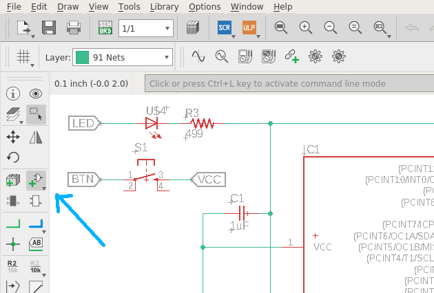
Components canbe added using the "Add part" button in the lefthand toolbar
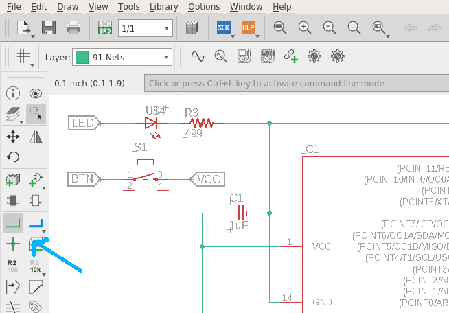
These can be connected using the "Net" tool to draw net segments onto the schematic.
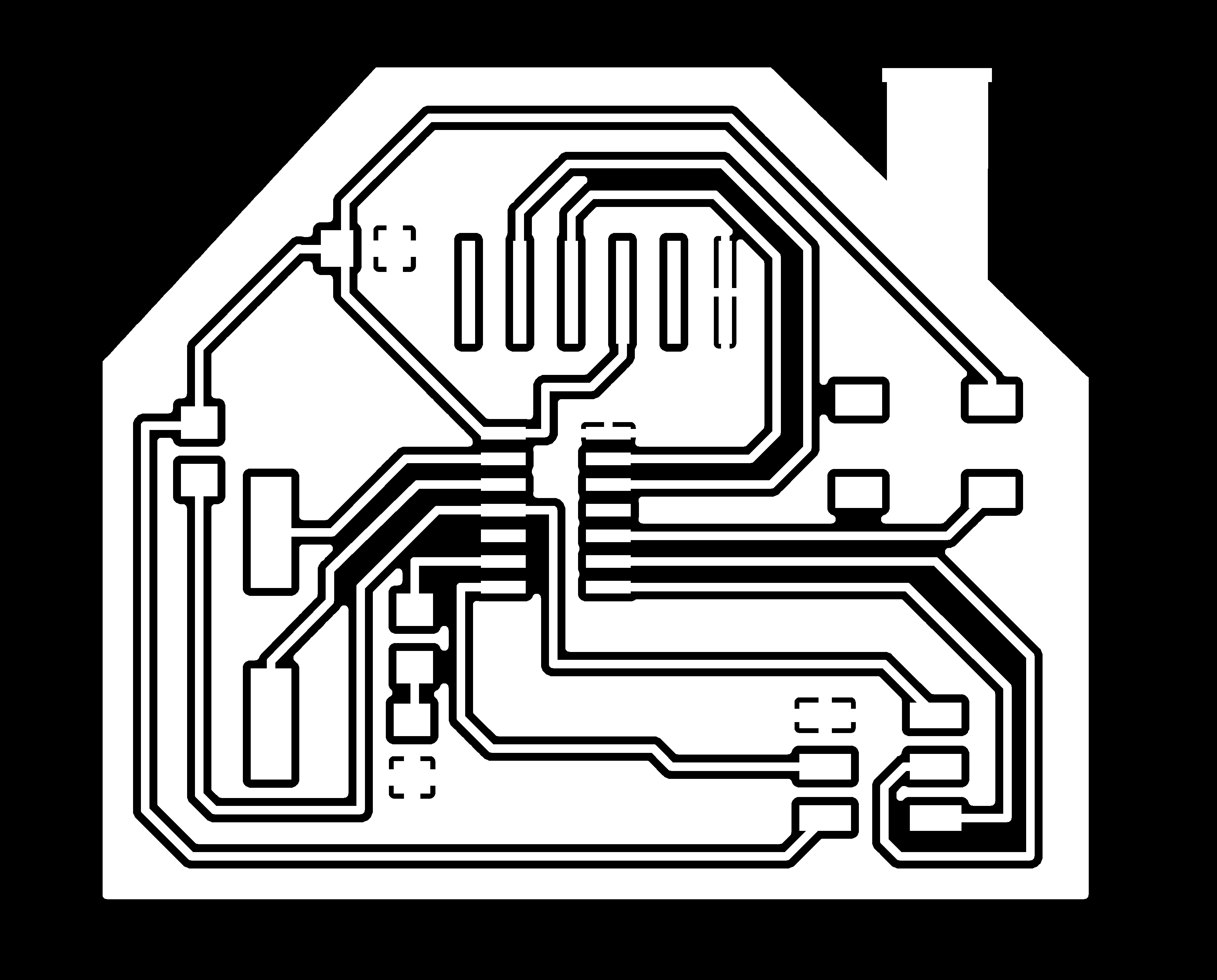
Instead of manually routing every single GND trace I decided to use the copper that is not beeing milled away as a common GND layer. For this I used the polygon tool in eagles routing view to draw a rectangle around the routed components and simply named it "GND", same as the GND net segment in the schematic view. Now I only had to click the ratsnest button and the rectangle would be included as the new GND layer. If there are any changes made to the other components after this step - like moving them around - one has to click the ratsnest button again to update the layer.
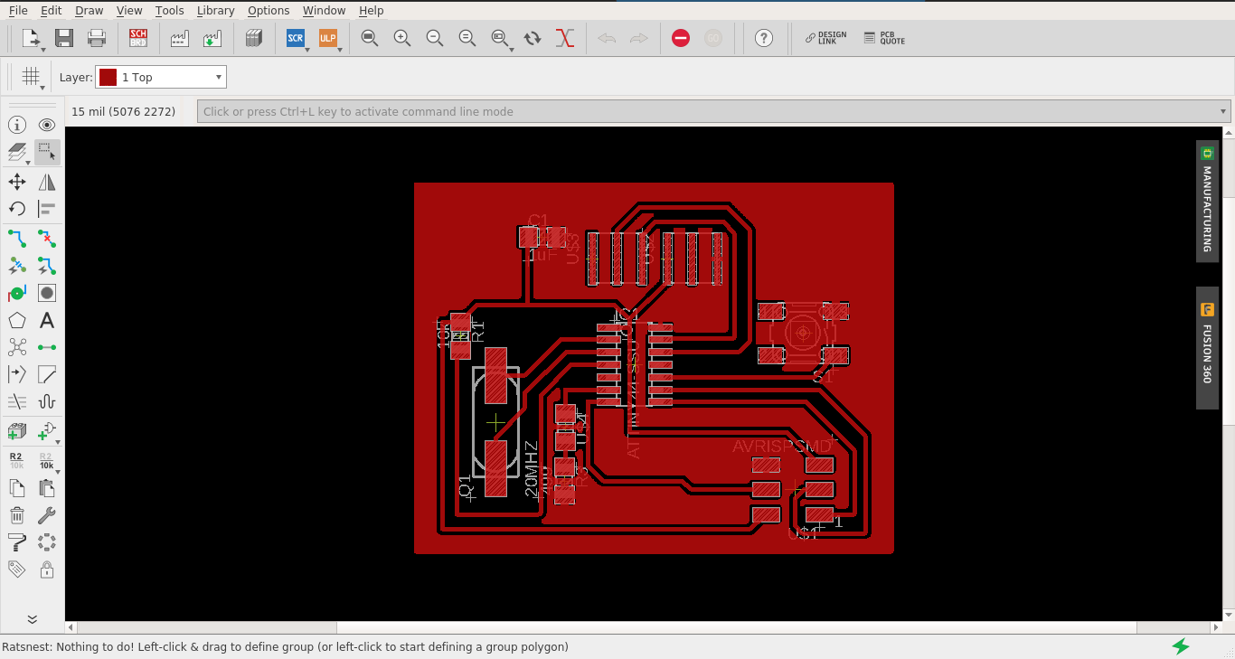
Routing view
hello.sch hello.brd(The mistakes I will mention later are fixed in this version.)
KiCad is a free and open source alternative to eagle. It can import eagle files and can export Gerber files. To import an eagle file just click "File" -> "Import Project" -> "EAGLE CAD". Just clicking trough the dialogs and using the default settings mostly worked for me.
Schematic after importing into KiCad
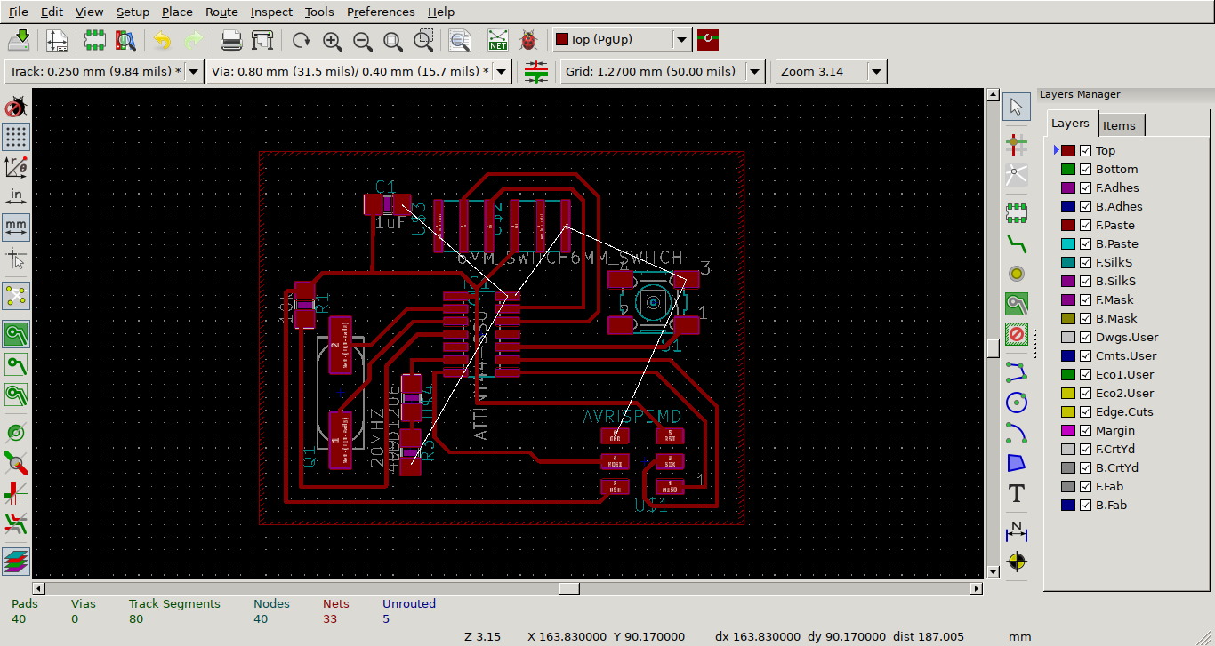
Routing view of Kicad. The routing created in eagle is preserved, except for the ground layer
We can get our GND layer back by making a right click on the rectangle, and selecting "Zones" -> "Fill".
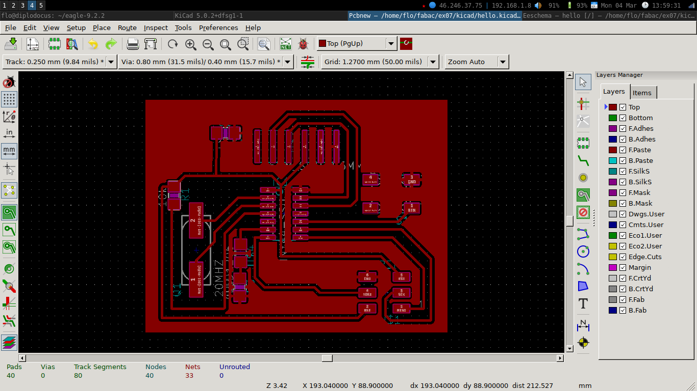
KiCad has a less polished interface compared to eagle, but as far is could tell the functionality is pretty much the same. The big advantage of KiCad is that it is free and open source, which also means that it can be used without connecting to the Autodesk cloud, creating an account or anything like that.
KiCad does not offer an option to export PNG images, but SVG can be used instead. In the end I used the export from Eagle instead. It also has no autorouting feature, but it can be used with an external autorouter.
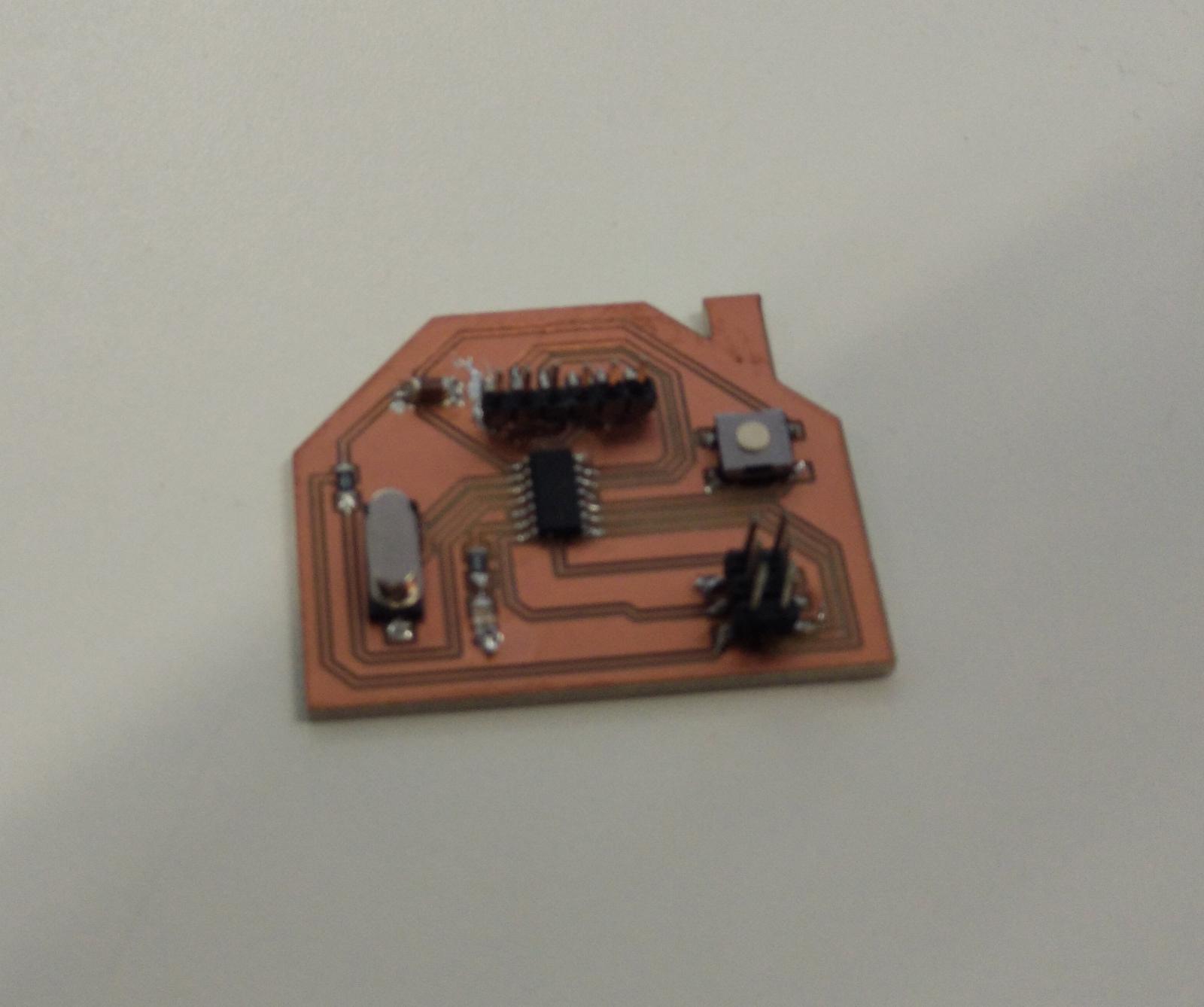
When exporting the board to follow the process described in the Electronics Production assignment I noticed that the cutout looked a bit like a house, so I also added a chimney.
From there on I just followed the electronics production process linked above.
During the design of this board I made two very bad mistakes. The first one happened when naming the net segments for RST and VCC. Because those two segments are very connected to each other I got them mixed up. Because of that my VCC input went to the RESET pin of the microcontroller, and the VCC pin of the microcontroller was only conneced trough a strong resistor. I managed to fix this by using a dremel to cut up the VCC trace and connecting it in a different way with a solder bridge.
Now I could burn the bootloader, just like I did before. But when trying to test the board I noticed the second mistake. I connected the button to a pin with an internal pull-up resistor, but did not connect it to VCC. With similar techniques as before I added a connection to VCC and a resistor. But with hacky fixes things are bound to go wrong at some point. When trying to reprogram the board my programmer could not read the device signature anymore. My bridge wire had touched something it wasn't supposed to touch and that blew the microcontroller.
After that I fixed the design of the board and milled and soldered it again.