Electronics
Production (week 05)
Group assignment: characterize the design
rules for your PCB production process. For this section reader is referred to Bomi Doh section.
Individual
assignment: make an in-circuit programmer by milling the PCB (AVR ISP),
program it, then optionally try other PCB processes.
Several
things have to happen before this week assignment minimum requirements are to
be met. The first step is of course, designing the PCB circuit before soldering
components on it and then program the programmer so it will serve its purpose
in future electronic programming to come.
For this part we
will be using:
Eagle software to
design the PCB traces. (Eagle software)
FlatCam to generate the
G-Code needed on the CNC side. (FlatCam
software)
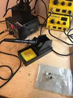
Soldering station
available in EchoFab
To program the
programmer itself, I opt for Arduino IDE software
BOM List:
|
Part Value Device Package Library Sheet |
|
|
|
C1 10pf CAP-US1206FAB C1206FAB fab
1 |
|
C2 10pf CAP-US1206FAB C1206FAB fab
1 |
|
C3 1uf CAP-US1206FAB C1206FAB fab
1 |
|
D1 3.3v ZENER_DIODESOD123 SOD123 fab
1 |
|
D2 ZENER_DIODESOD123 SOD123 fab
1 |
|
IC1 ATTINY44-SSU ATTINY44-SSU SOIC14 fab
1 |
|
R1 1k RES-US1206FAB R1206FAB fab
1 |
|
R2 100 RES-US1206FAB R1206FAB fab
1 |
|
R3 100 RES-US1206FAB R1206FAB fab
1 |
|
R4 499 RES-US1206FAB R1206FAB fab
1 |
|
R5 0ohm RES-US1206FAB R1206FAB fab
1 |
|
R6 0ohm RES-US1206FAB R1206FAB fab
1 |
|
R7 10k RES-US1206FAB R1206FAB fab
1 |
|
U$1
AVRISPSMD AVRISPSMD
2X03SMD fab 1 |
|
U$2 CRYSTAL CRYSTAL 2-SMD-5X3MM fab 1 |
|
U$3 USB_MINIB USB_MINIB USB_MINIB fab
1 |
Designing PCB:
Normally one needs
to select all components needed, declare the links between them and then
generate the routes. This time, our facilitator, Francois Auclair
provided us with the full eagle project file and therefore we did not need to
attend this step.
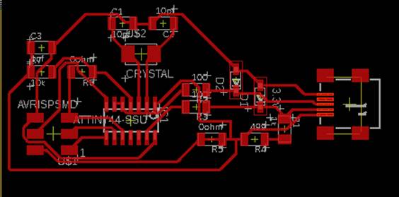
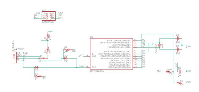
Find here views of
the schematic and board
From
this point forward, the necessary steps were done individually as follow (Onto FlatCam!!):
Into
Eagle project space a Gerber file was generated and fetch into FlatCam. This step needs to happen to translate, with
milling specification, the Gerber file into a (metric here) CNC G-Code file before
we can carve the PCB.
Specifically,
we used here the copper top Gerber
file into FlatCam software.
Here
in EchoFab, we retain by default the following
settings (preference) into FlatCam to mill our boards:
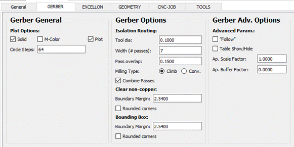
·
Tool diameter: 0.1
·
Pass number: 7
·
Pass overlap: 15%
·
Milling in climb mode
·
Combine passes
Next step is to set geometry before we
can generate the G-code itself.
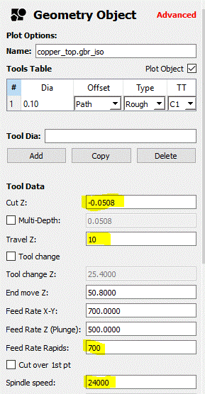
Critical for us are,
·
Cut Z depth: 0.0508
·
Travel Z: 10
·
Feed rate rapids: 700
·
Spindle speed: 24000
Next
step is to generate the CNC job object, transfer it to the CNC machine and cut
the board.
Note: In reality two files are
generated with more or less the same settings, one is the trace file (described
here before) and the second one is the profile (perimeter) of the PCB. This is
essentially done in the same manner with a bigger tool and single Z pass, only
deeper, to cut the piece out.
The
CNC machine we are using is made so that the X and Y axes homing is
mechanically assumed. On the other hand, Z homing position has to be done
manually. Setting Z coordinates take
advantage of the conductivity of both the milling bite and the copper surface.
Essentially Zero position is done by using conductivity detection on a
multimeter. One probe in contact with the copper board, the second with the
bite waiting for the conductivity to show up on the multimeter while manually
the Z probe system is lowered. Upon contact we know, if steps are small, that
we are at the first limit of contact and Z relative positioning can be set.
Thereafter,
carving trace is only a matter of executing the G-code, supervising the process
in case of a fail and make a quick quality control assessment (visual
inspection) before we are to solder the components onto the board.
Miscellaneous
images of the milling process:
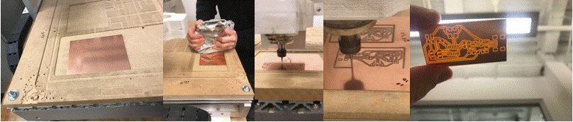
NB: Annie Ferlatte
and I have traced and cut-out our board in a single sheet, this was a first
attempt to be cutting two boards in a single run, saving raw material.
Essentially this implicates noting coordinate for the first board to be carved,
then carving the second before both are extrude of the surface while re-using
previously noted home position of the first one.
Satisfied
with the board cutting, it’s now time to turn to the welding of the components
onto the copper traces.
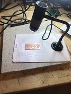
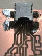
Surface
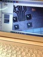
mount soldering is a technic to acquire, but in my case the challenge was very
much it, a true challenge! I have lost my reading glasses and cannot properly
see were I’m to solder. I know how but I simply can’t see well. So, after
several attempt with the aid of a USB microscope I had to come to turn with my
handicap. I managed to solder the parts on the paths, but results were far from
being satisfactory. Some welding I’ve done, aiming at the pad before being
blinded by the soldering rod, hoping, praying even that I would get it bull
eye’s, led some splattering all over the place. Eventually I opt for liquid
welding and got better results but not on this journey (see upcoming weeks).
Miscellaneous
images of the soldering process:
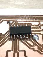
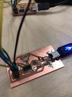
But
for now, the board is soldered and now we need to program it so it will become
an AVR ISP.
The
sequence of command is an easy one:
·
Lorem ipsum dolor sit amet, consectetuer adipiscing elit.
Maecenas porttitor congue massa. Fusce posuere, magna sed pulvinar ultricies,
purus lectus malesuada libero, sit amet commodo magna eros quis urna.
·
Nunc viverra imperdiet enim.
Fusce est. Vivamus a tellus.
·
Pellentesque habitant morbi
tristique senectus et netus et malesuada fames ac turpis egestas. Proin
pharetra nonummy pede. Mauris et orci.
·
Aenean nec lorem. In porttitor. Donec laoreet nonummy augue.
·
Suspendisse dui purus, scelerisque at, vulputate vitae,
pretium mattis, nunc. Mauris eget neque at sem venenatis eleifend. Ut nonummy.
A
note: Here are presented the overall process we used answering this week
assignment. But in reality, for a fairly long time all team members here at EchoFab had a problem with the programmer we were trying to
make. Facilitator from our lab and others joined their neurons trying to
understand what was going on. After troubleshooting all possibilities, it was
realized that the Zinner diodes we were using were
rated to high for our needs. Replacing the faulty parts with the right ones,
solved the problem and we were able to move forward.