Networking and communications
Assignments
#1 - Design and build a wired or wireless network connecting at least two processors
This week, my targets are the followings:
- Design and make my first double side PCB.
- Integrate a BLE (Bluetooth Low Energy) device on that board
- Demonstrate how my board can exchange information with another device over BLE. For that part, I will use off-the-shelf components first, to be sure my SW has no bugs and then my homemade board for the final demo.
References
Lecture
This week is about electronics and more specificaly abour all kind of outputs:
- All you need to know about double side pcb
- Discovering the SKB369 BLE board
- Discovering the SK EVB development board
- Programming the firmware using Arduino IDE
- Testing the entire system and measuring power consumption
Recitation
This week is about ...
Topics covered (course) Video recording (course) Video recording (recitation) Students and Labs My filesLearnings
Designing with own PCB
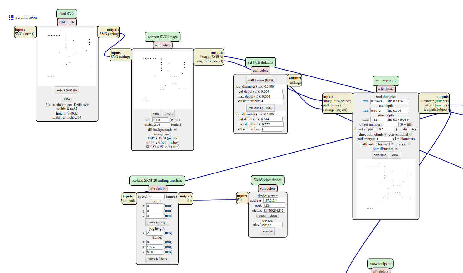
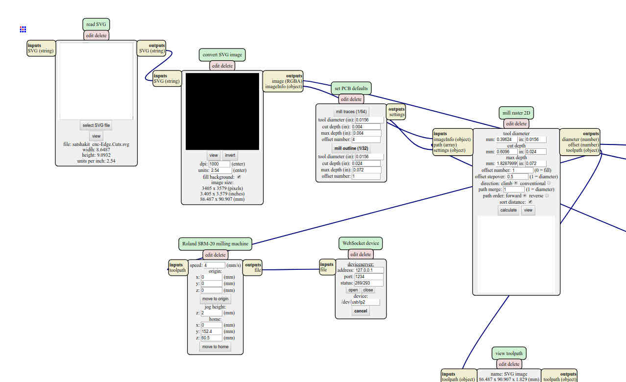
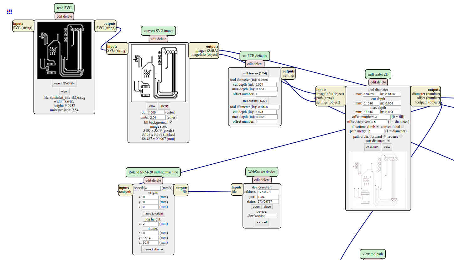
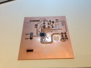
In the last two weeks, I made a PCB starting from an existing design (the Satshakit). Now, I feel ready to go on my own. I could probably make it work with a single side PCB for this week but I know I will need a double side PCB for my capstone project and I want to give it a try.
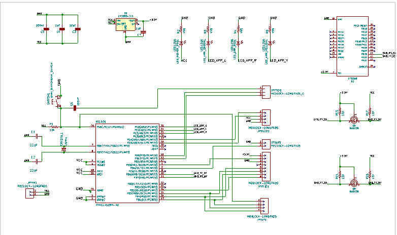
As for the Satshakit, I will design around an ATMEGA328P. There is an additionnal challenge this week since the BLE board I want to use does not support 5VDC. This is not just a matter of feeding it with 3.3VDC but also to build an 5V-3.3V interface for every single wire connected to it (check on the bottom left part of the schematic)
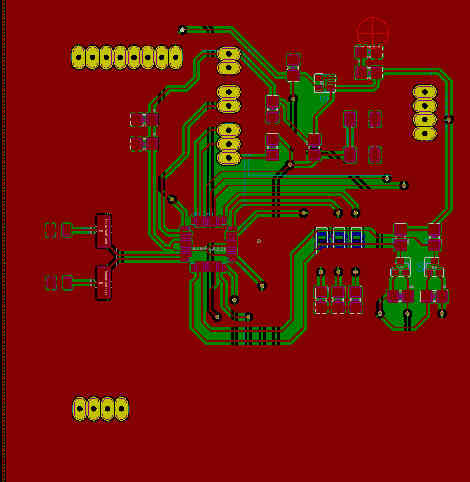
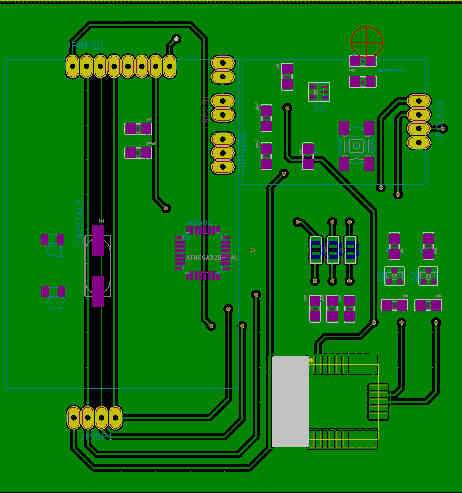
And here is the PCB layout
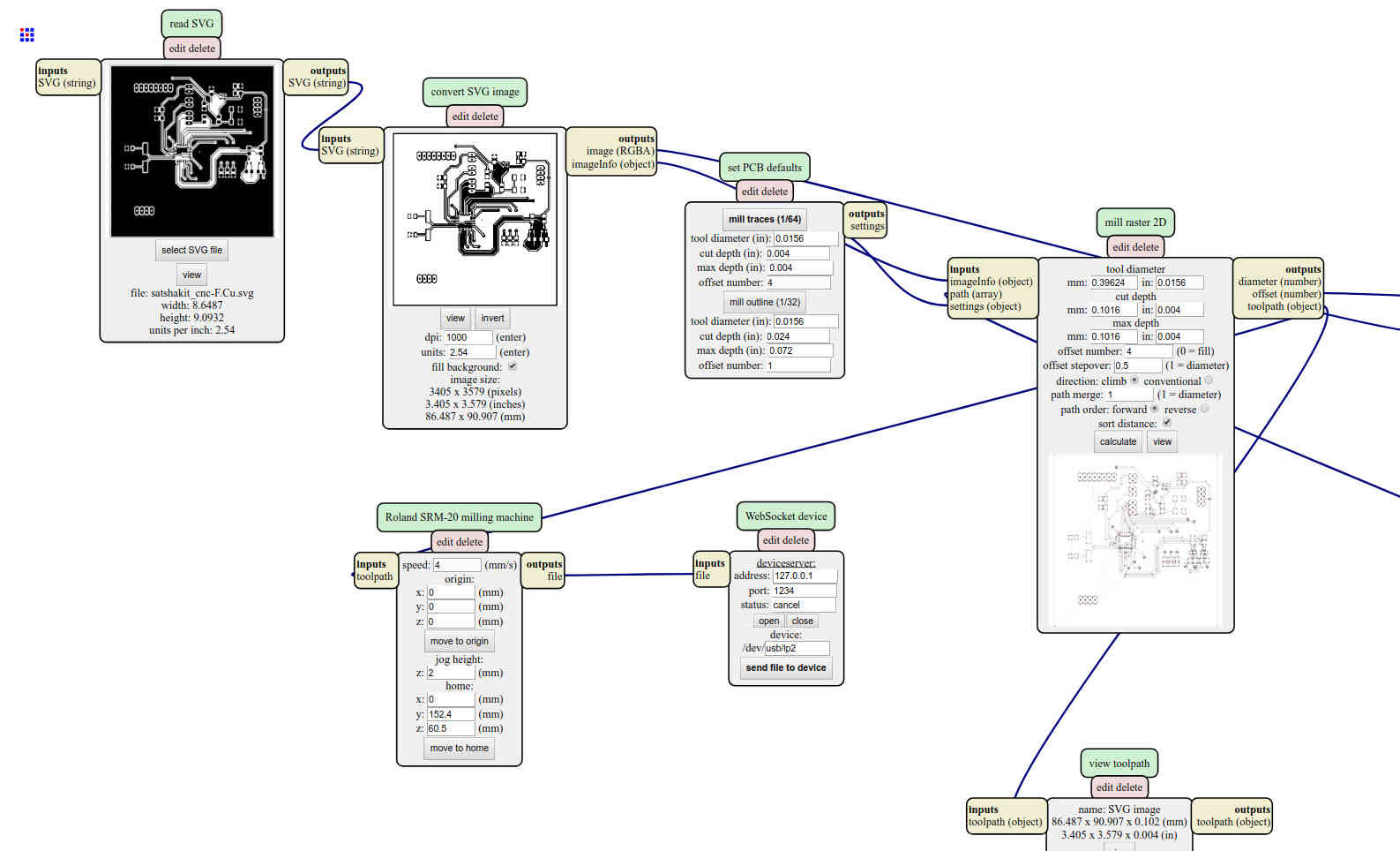
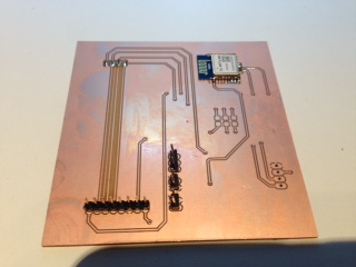
The production process has 4 steps: front-side, holes drilling, perimeter cut. Then flip the board and engrave the back side.
This was my first experiement with double side board and vias. I used small eyelets for the vias. It is required since there is no conductivity whithin the small holes that are drilled in the PCB. The eyelet is like a copper conduit that connects both sides.
I struggled a lot with the alignment. To mill the back side of the PCB, I have to flip it but it has to be very precise to make both sides of the vias to fit exactly on the same place. My first strategy was to drill the mounting holes more deeper (in the MDF support). It could work but it killed my engraving bit. Then I realized I could just flip the target pcb without flipping the entire pcb blank, it is not that difficult to keep it centered.
Having a double side PCB helps to solve the issue I had last week with my connectors. Now, I can solder them on both sides
As per the instructions, I should punch the eyelets and then apply some solder on it, on both sides. But the tool to punch the eyelet is so large that I cannot see them and the result is not always great.
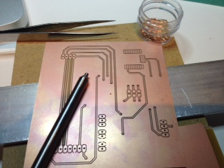
As usualy, a few things went wrong. The pcb shown here is the 5th attempt, all others ended up in the recycle bin. Here is the weekly story:
- Attempt 1: one issue with spacing between traces and one issue with the SKB369 footprint. Even if Kicad rules checker says it is ok, I still ended up with a board with no space between traces at a specific location (not everywhere) Learning = check more carefully the mods output. It was visible, I could have save time and material
- Attempt 2: there are two sides now but it does not help if you route traces to the connector on both sides. Then you still have to solder under the connector plastci cap and it ends up with a plastic mess and/or a loose connector Learning: keep one side free and place the connections on the same side as the soldering.
- Attempt 3: my home made reflow oven is not that bad with single side boards but it does not work with double side boards. Learning: I should better solder the components manually.
- Attempt 4: no double side tape anymore... I tried with another rool I had, it was good for the front side but then the pcb moved .. and there is no easy way to reposition it. Learning: never start something serious on sunday afternoon when everything closed at 5 PM
- Attempt 5 : still a little problem with GND connector that should be soldered on both sides. Solution is to add more vias. Need to add a temporary wire to patch but it looks ok now
Discovering the SKB369 board
The SKB369 is a highly integrated Bluetooth 4.2 BLE module, designed for high data rate, short-range wireless communication in the 2.4GHz ISM band. Also, SKB369 support ANT Protocol. The module is based on Nordic nRF52832 radio Transceiver IC, has a 32 bit ARM Cortex-M4F CPU, Flash memory and analog and digital peripherals. The SKB369 provides a low power and ultra-low cost BLE solution for wireless transmission applications. The SKB369 also has a NFC-A tag interface for OOB pairing.
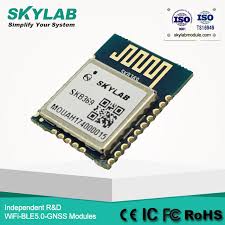
The HW goes as the datasheets says but... the firmware installed on it does not support NFC-A tags and does not support BLE MESH neither. It is possible to re-flash it but it would take more time than I had this week.
Note: all datasheets are within the zip file for this week
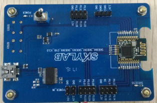
Discovering the SKB360_EVB board
This is a development board with a plug and play slot for SBK mini-boards. The biggest advantage is to be able to swap modules without multiple soldering/desoldering operations.
Communicating between a MCU and the SKB369
One possible way is to leverage the software installed by the Chinese supplier on the board and their command set.
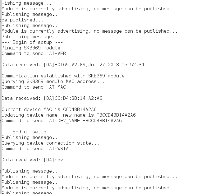
First, we need to setup the HW and the wiring between the boards. I started with simple elements: a SKB360_EVB with a preloaded SKB369 in the card slot, an Arduino Uno, a logic level converter and two wires between the SKBs and the Arduino The converter is really important since the SKBs do NOT support 5VDC
There is an On/Off switch on the SKB360_EVB. Once turned on, the SKB369 will start advertising as nRF52832 (the part provided by Nordic SemiConductor
Now, let's start the Arduino IDE and try to communicate with the board over an UART link. Here is what we want to implement:
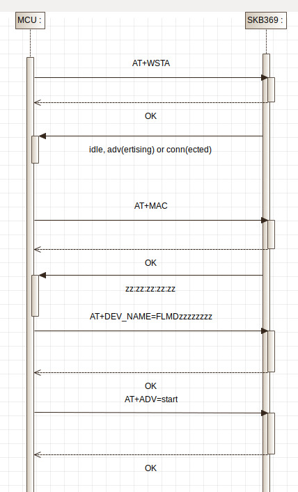
And here are the details
- WSTA : query the SKB369 in order to figure out what he is doing. The answer can be: I'm idle, I'm advertising or I'm connected
- MAC: query the current SKB369 MAC address. We need this since it will be used as a unique identifier later
- DEV_NAME=... : here, we set a name we want to be used for advertising. Initialy, all SKB369 use the same name (nRF52832) and there is no way to distinguish them)
- ADV=start : from here the SKB369 will advertise, i.e let everybody know he is on line
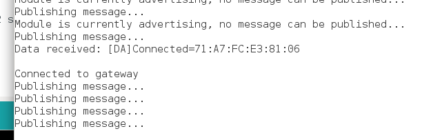
Let's have a look now on what happens on the gateway (Raspi) side now. At startup, the gateway enters in a loop where he is listening and waiting for Fab Buddies to talk to him. As soon as he discovers one of them (based on the fact they advertise themselveswith a name starting with FLMD, the gateway will try to connect back. Here is how it goes then on the Fab Buddy side
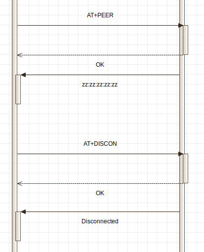
And here are the details
- PEER : this is a pairing request, i.e an answer to the request we just got from the gateway. If everything goes well, both devices are paired from this point
- But .... what if a malicious device tries to pair with our pour little Fab Buddy ? We need a mechanism to say... No, thanks ! (DISCON) For the prototype, I will simply compare the gateway MAC address with something hard-coded. In the real world, it should be part of a provisioning procedure where a Fab Lab admin tag is used to configure the Fab Buddy.
For this week, the last part is to demonstrate I can exchange information between Fab Buddies and the Fab Buddy Gateway. As a proof of concept, I will implement a simple heartbeat mechanism. The Fab Buddy will report himself to the gateway on a regular basis. Here is the sequence:
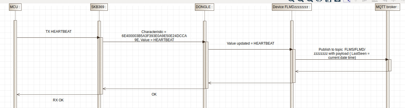
And here are the details
- From the code running on the MCU, we send a simple keyword HEARTBEAT over the UART link to the SKB369
- The SKB369 will turn it into a BLE Characteristic (if you don't know what a characteristic is, read this on Bluetooth SIG web site. This is a fundamental concept within the BLE world)
- A program running on the gateway (assuming he is connected and paired to the SKB device) will be notified and get that keyword
- Then he will post a message to a queue. That part is not fundamental here but if you should read this if you don't know what message queing and MQTT protocal are
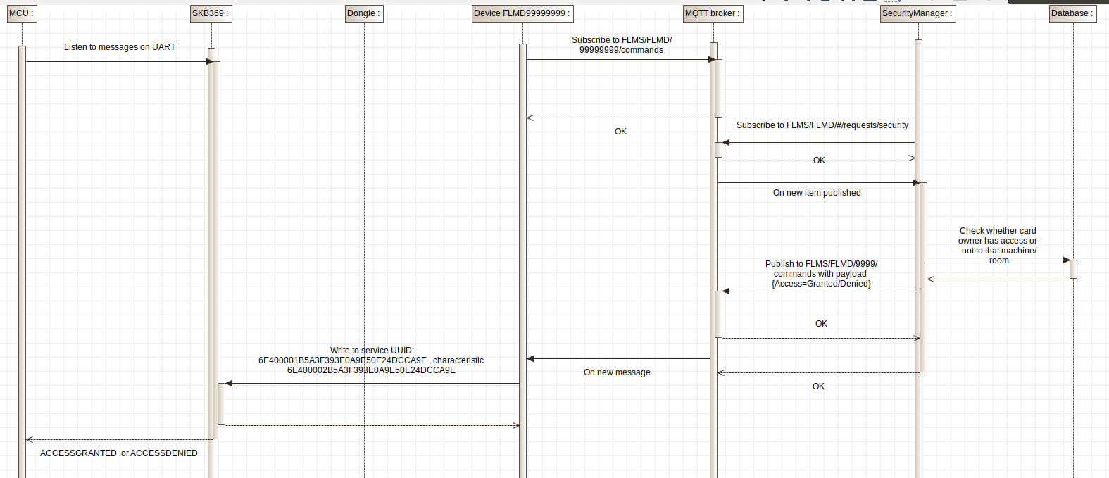
Here are some other sequences I will decribe in the coming weeks and that I want to implement for my capstone project. The first one describes what happens when a RFID tag is swipped. One important point to mention is the fact that the communicaiton is message based, i.e there is no need to wait for the gateway to process a request. The request are put in a queue and processed when it is possible, depending on the laod on the gateway. The response is sent back to the Fab Buddy as part of another message.
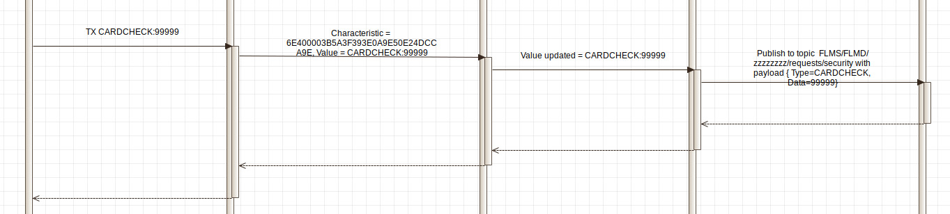
This one is the answer provided by the gateway once a card check request is processed
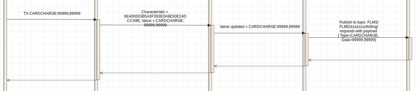
This one is a request sent by the Fab Buddy to charge an expense to a user account
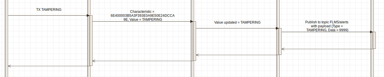
And the last one is what happens when tampering is detected on the Fab Buddy side. I don't know yet how to detect tampering from HW point of view but I will find a way
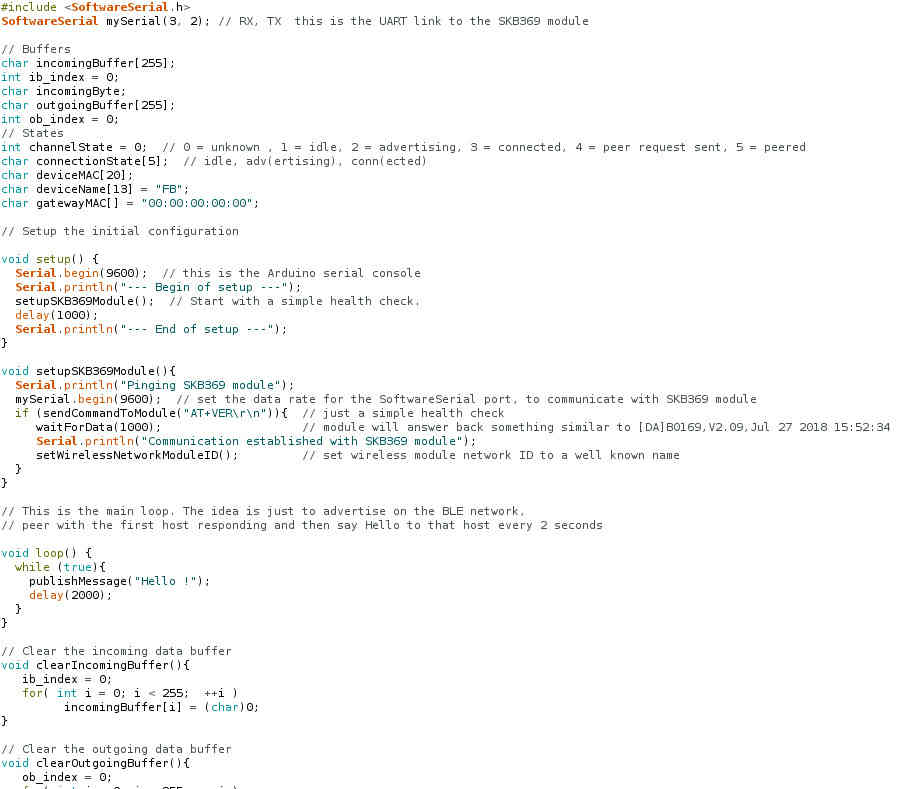
The source code is here and is fully documented. Here is just a part of it to give an idea of how it looks like
Wrapping everything together and testing it
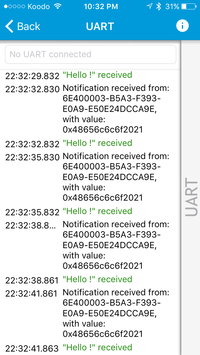
For this demo, my board is on one side and my iPhone on the other side. The nRF Toolbox (from Nordic) runs on the iPhone and my code runs on the ATMEGA328P. At startup, my board will set a unique name (based on SKB369 MAC address) and start advertising
Then I select the advertising device and I press on Connect button on the iPhone. My code continues with a peering confirmation
From there, messages are trasmitted from my code to the iPhone App. Here is the app log
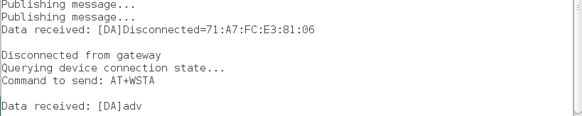
If I kill the iPhone app, my code with resume advertising
Achievements
#1 -Send a message over a network
Done. Both sides have (statisticaly) unique names (based on ther MAC address)
#2 -Send a message between two projects
See here
Capstone
#1 - Send a message from device to gateway and read a message sent by gateway
Done