Electronics design
week 7
February 27, 2019
This week, we are designing our first electronic circuit. We have to rely on the Hello Board circuit and we have to add at least a button and a led. For that, it is necessary to design the schematic, then to design the board, to mill it and to solder it.
Design the Hello board
Design the schematic
Eagle is a EDA program. It is a software that is used in electronic board design. It is the commercial version of KICad which is the open source version. Here is the interface of Eagle. First, we must establish the connections between the components in the schematic. It is with the schematic that the assistant will help us to design the board and make the routes. I decided to use this software because I had already worked with it in the past.
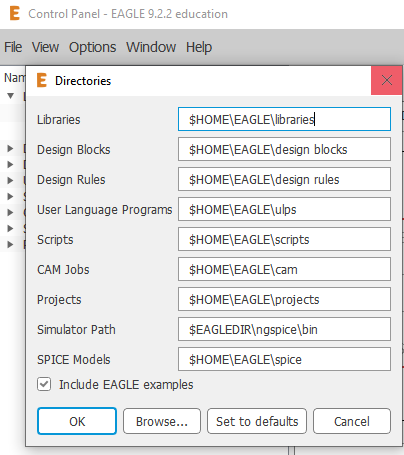
Eagle has a lot of component library but it does not have them all. That's why we need to add the Fab Academy library to access the right component of the Hello Board.
I put a copy of the library in the files of this telechargeable at the bottom of the page. To import the library, just go to the option menu and choose directories. This lets you know where to drop the Fab Academy library.
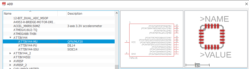
The components are divided into two parts. There is the drawings of the piece in the schematic and also the footprint of the component on the pcb. Sometimes we can select the right component with the right design for the schematic but does not have the right footprint for the pcb. You have to be very careful.
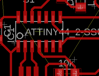
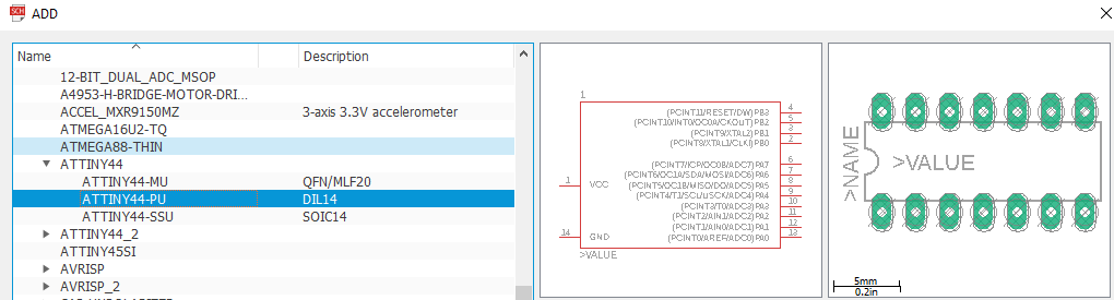
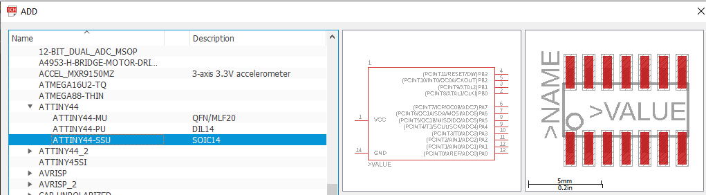
Here is an example of the attiny44 we use in HelloBoard. So there is 3 times the same schematic of the component with 3 different footprint
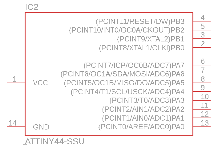
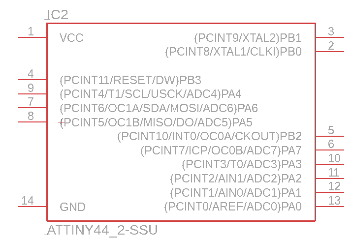
A little trick for schematic drawing is to take all the components that we will have in the schematic to better position them. It's also a way of seeing the complexity of design. Also, you have to put all the input at the left of the schematic and the outputs at the right of the schematic. It's the same rule when we create our own component.
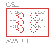
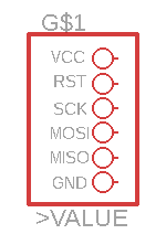
To respect the rule I just mentioned that all inputs are on the left and all the outputs are on the right. I had to redesign the schematic of Attiny44 and AVRISP. The original is on the left and the new is on the right.
Now it's time to get all the components we need in our schematic.
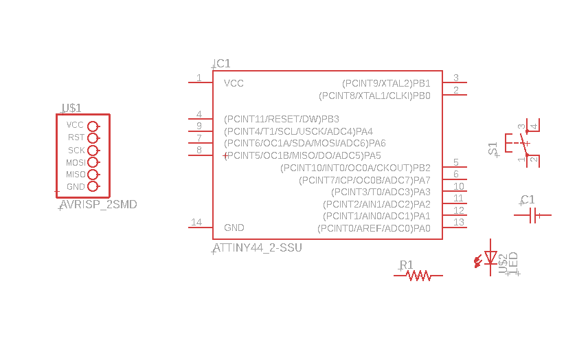
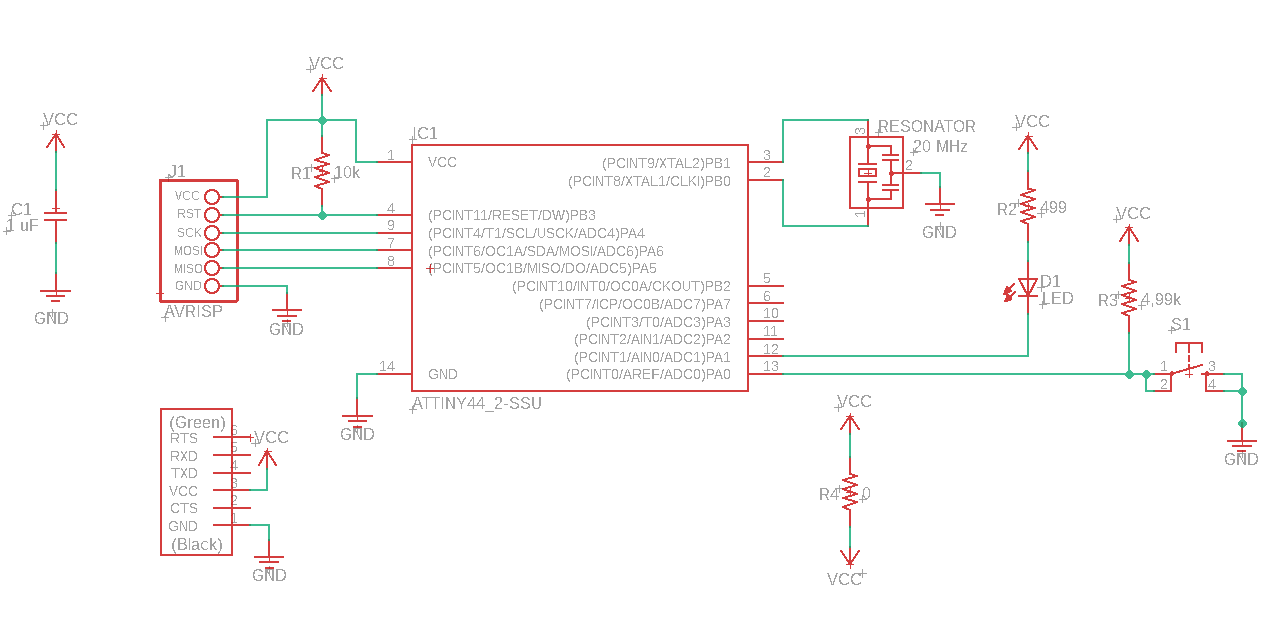
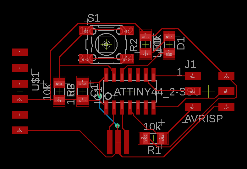
Here is the schematic with all the components and connected together. It is possible to connect components together without necessarily being side by side. For example, the capacitor C1 must be as close as possible to the Attiny44 on the pcb but C1 is only connect to the VCC and the ground so we can put it elsewhere in the shematic. This technique makes the schematic less messy. Also, all components are well placed and straight. Again, the inputs are on the left and the outputs on the right
Design the board
After the schematic is finished, it is now time to design the pcb. Eagle when you create the board file, puts all the components in the corner of the sheet as on the imgae below. The yellow lines that we can see are the future connections that we have to connect together.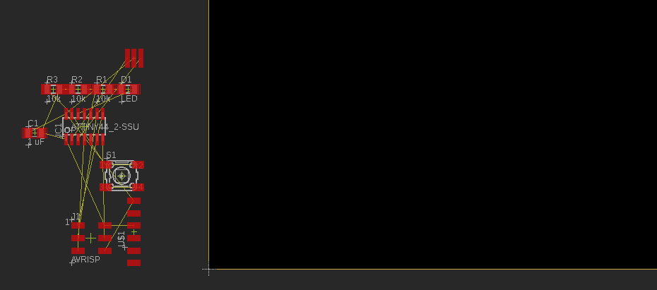
Like the schematic, the components must be placed first to facilitate the work. It is important to put the components that have the most connection between them are side by side. Also, some component must be close to each other to eliminate some electrical problem. The resonator must be ready for the Attiny44 and the decoupling capacitor C1 must be ready for attiny44.
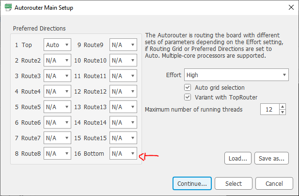
In eagle, there is a autorouter tool. This tool is used to draw routes automatically. You just have to choose the options as in the window and click on continue.
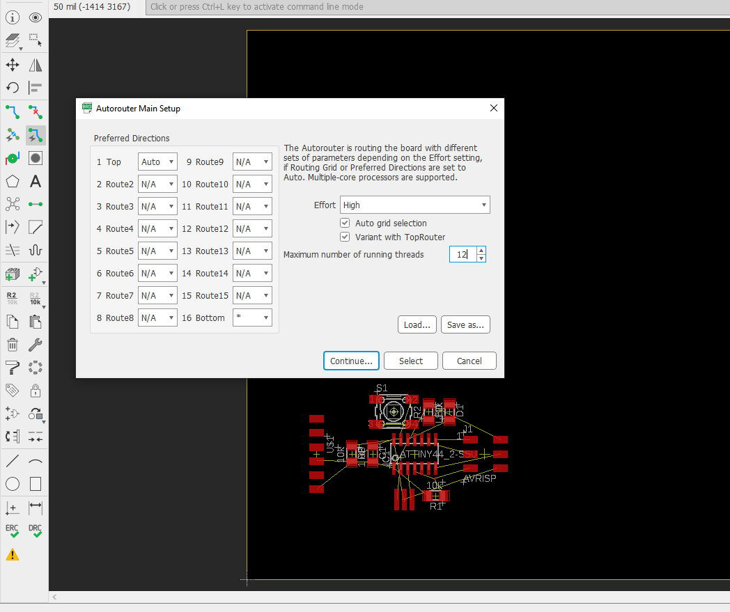
The highway will try to make all the roads by trying several possibilities. If all this returns to 100% it means that the circuit is completed.
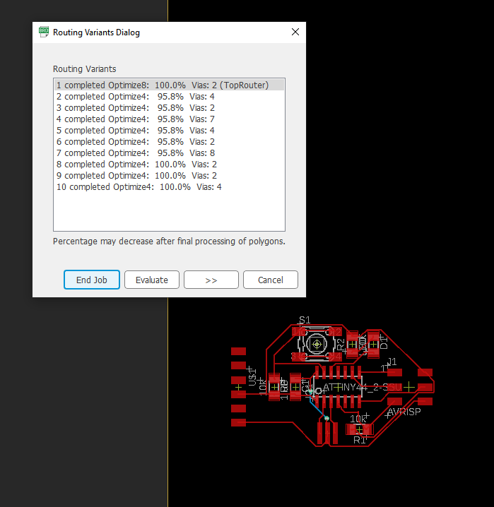
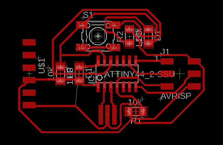
Here is the result. The routes in blue represent a trace on another layer of the pcb. Pcb is composed of layer to be able to help people to build pcb more complex. In our case, it is only possible to make pcb at one layer with the CNC. When a pcb is mult-layered it's like we've drawn several pcbs and pasted them together to make a bigger pcb. The connection between layers is done with vias. It's the two little green circle that can be seen at the end of the blue line.
The reason for this second layer is a bad choice in the options of the highway. You only have to say N / A for the bottom layer and there will not be more than one layer.
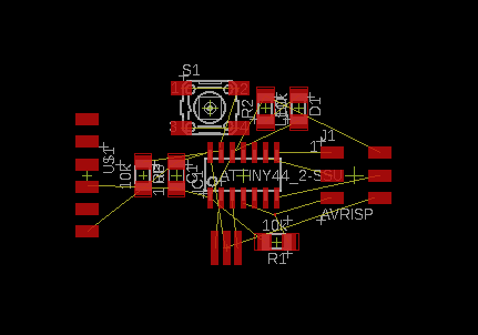
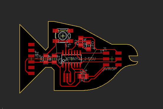
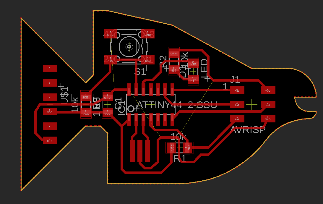
Here is the result on one layer. It's good as a result but looking at the pcb I noticed that it had a fish shape. So I will manually make the routes to give an original shape to my pcb.
With the line tool on the dimension layer, I drew the outline of the pcb in yellow. This will be used to make a ground surface on the pcb.
With the polygon tool on the top layer that is the same roads. We must draw the outline of our pcb to delimit the ratsnest. We can see under the yellow line there are now red dots.
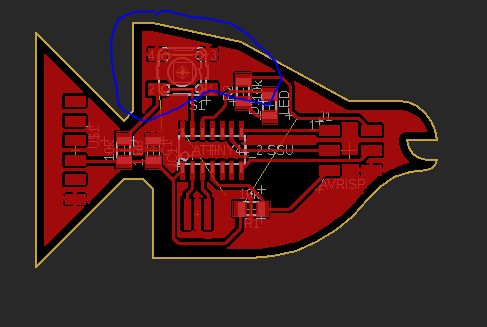
at first sight, the board looks good with the ratness which is a ground. The most important thing with a ground is that all grounds must be connected. So if you look closely in the blue circle, you can see that the ratnest's ground section is not connected to a ground.
I enlarge the dimensions of the pcb for the ratsnest can connect. By doing that, I had a problem with a VCC. I had to put a resistor jumper. This is used to pass a trace under a 0 ohm resistor. It does not affect the circuit at all, but helps to jump the road over another road. It is impossible to add a component on the board if it is not in the schematic. So we have to add it to make the changes on the board.
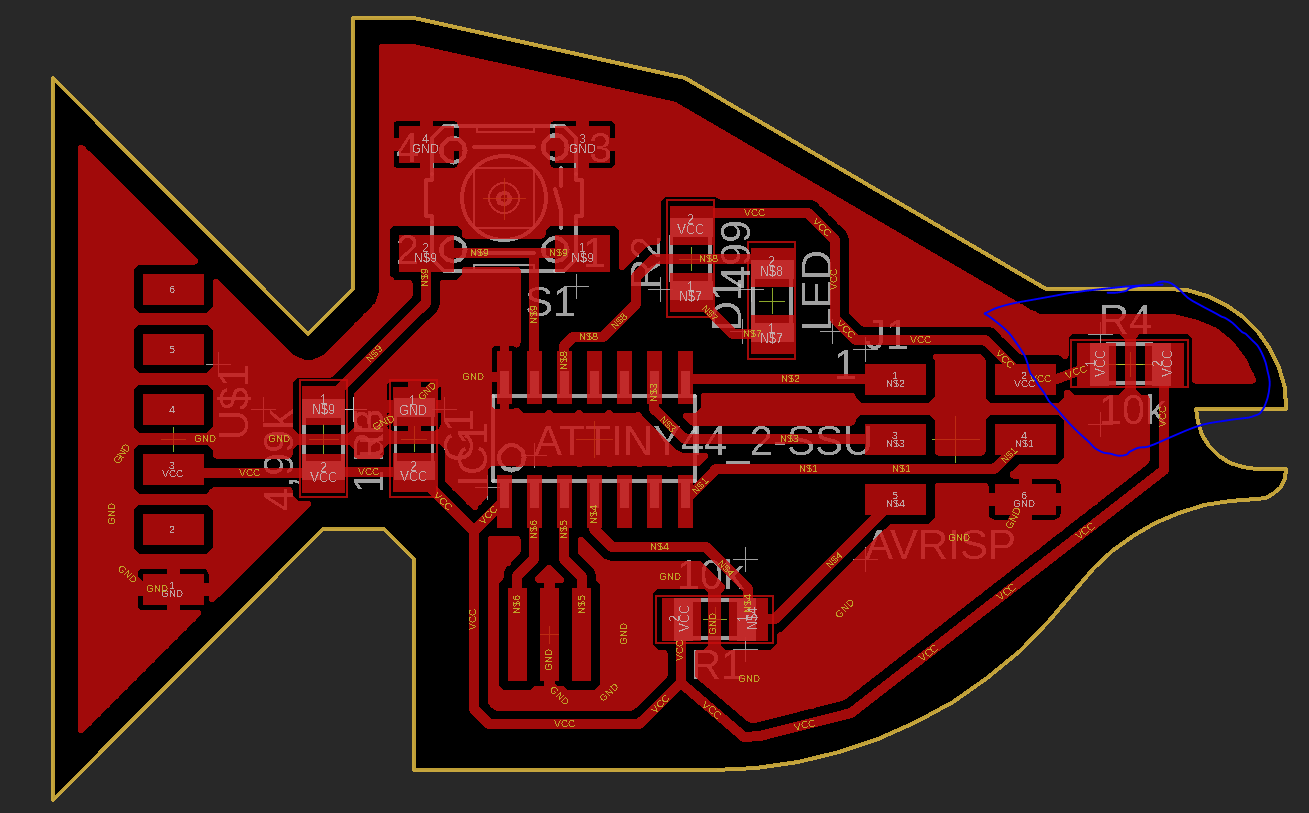
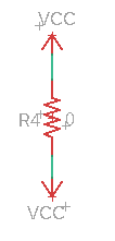
In the schematic, at the location of your choice, you need to connect a 0 ohm resistor on the signal you want to jump over the other. Here, I want to jump the VCC. So I will connect two VCC together with resistance. As in the picture below. Subsequently, I will be able to do as on the final shematic.
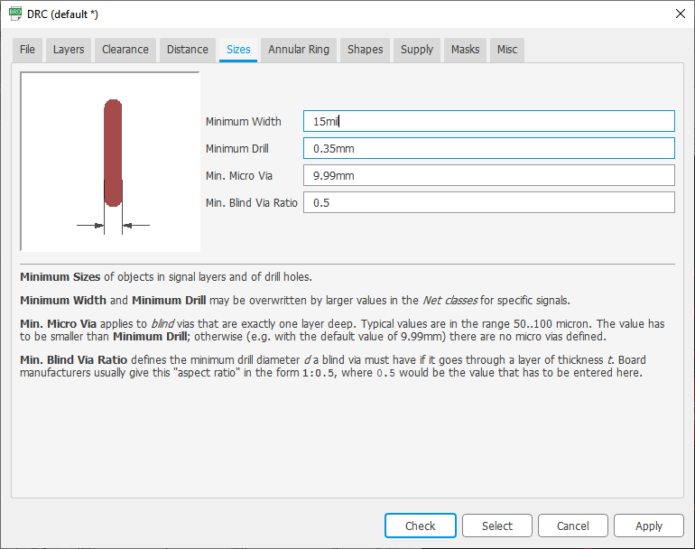
In Eagle, there is a tool to check that all distances are correct between components and roads. In order for the tool to correctly check your circuit, it must be configured with the right design rules. General rule, a distance of 15 thousandths of an inch between the pads and the wire is raissonable for the type of circuit we want to do. For this small circuit, we do not use vias so it is not necessary to change with the other value.
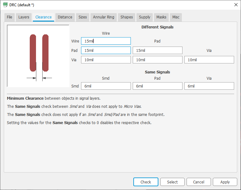
The other parameter to adjust for our circuit is the width of the trace. According to the table below, for 1A it takes a trace of 10 mil wide. To leave a margin of safety, we will trace 15 mil. The other parameters are not necessary for our circuit.
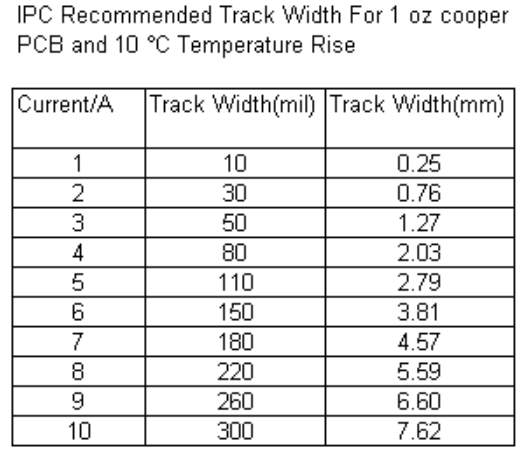
Reference: https://www.mclpcb.com/pcb-trace-width-vs-current-table/
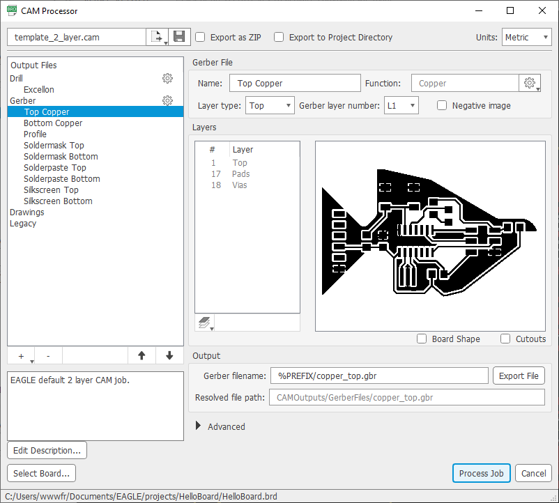
The last step in Eagle is to export our circuit to gerber file so that it is compatible with the software that prepares the circuit for milling. It is important to take the layer that we create our circuit which is the top. The software will now export our gerber file.
Preparation of the board for milling
In the FlatCam software, you need to import the Eagle gerber file. I use this software to be able to generate the gcode that the CNC will be able to read. The input parameters are subjective but with the experience of other people in the lab, these are the parameters that have been suggested for a good result.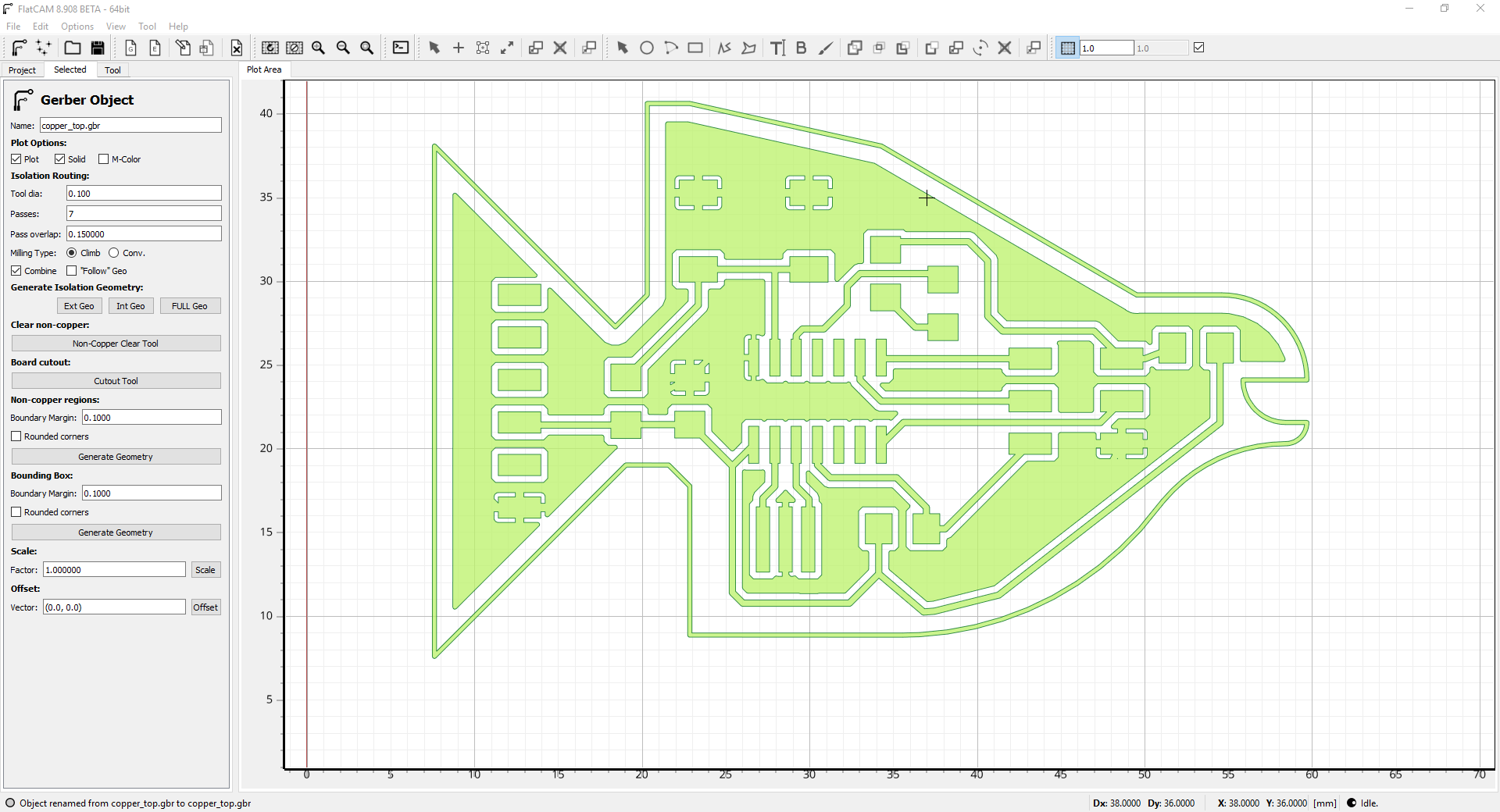
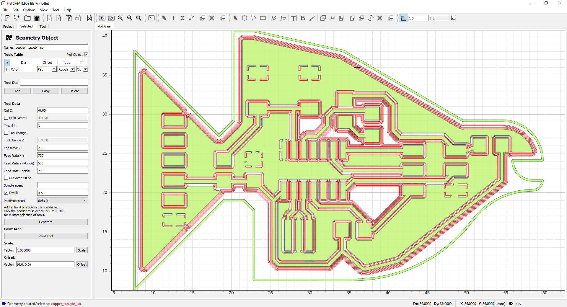
The first part to be generated is part of the electronic circuit. For better accuracy, I do not mill the board with the same width of tools. For the circuit I use a 1/64 tools for traces. With the size of the tool, we will make up to 7 passes. We will also follow the outer line of the tracks so as not to change the size of our traces.
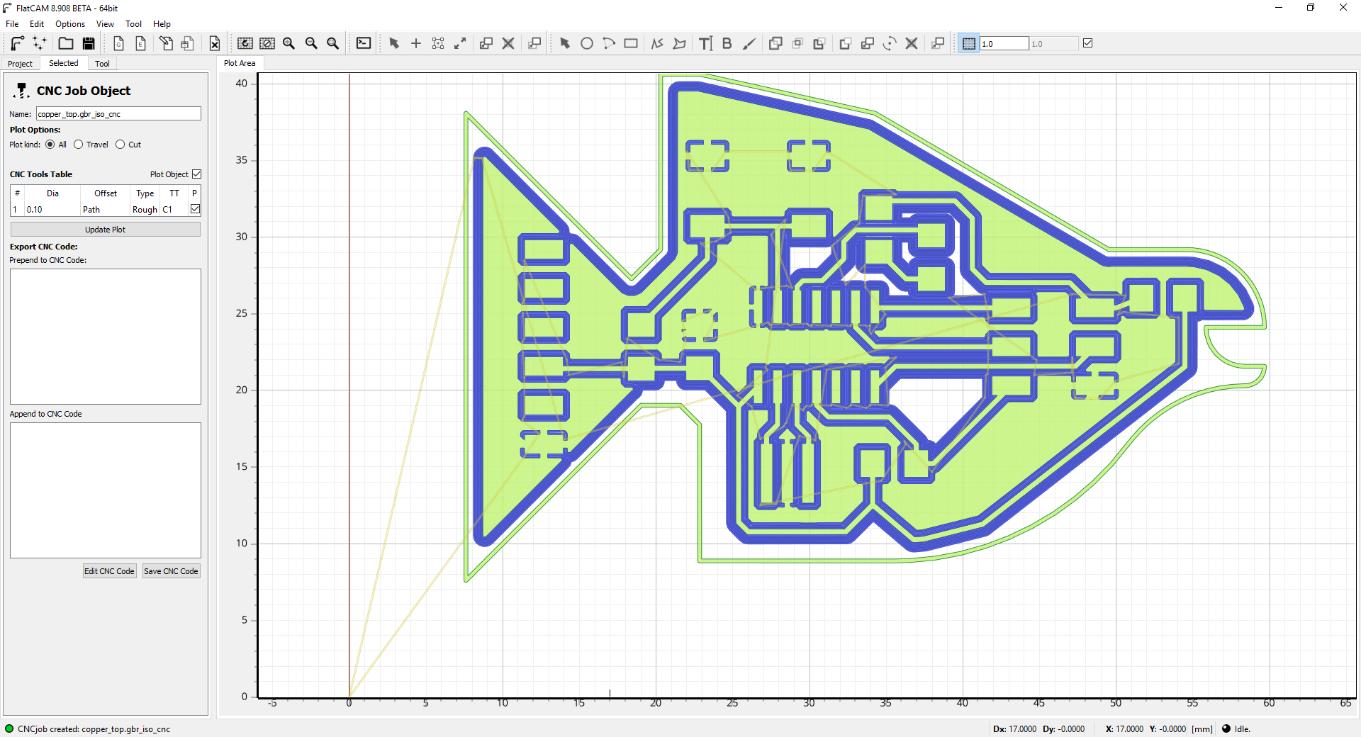
Now we generate the Gcode for the first part of the job.
Now you have to set the parameters to cut the contour of our circuit. For this, I use a tool of 1/32 width. It is important to make the cut in several passes deeper and deeper and following the outside lines of the circuit.
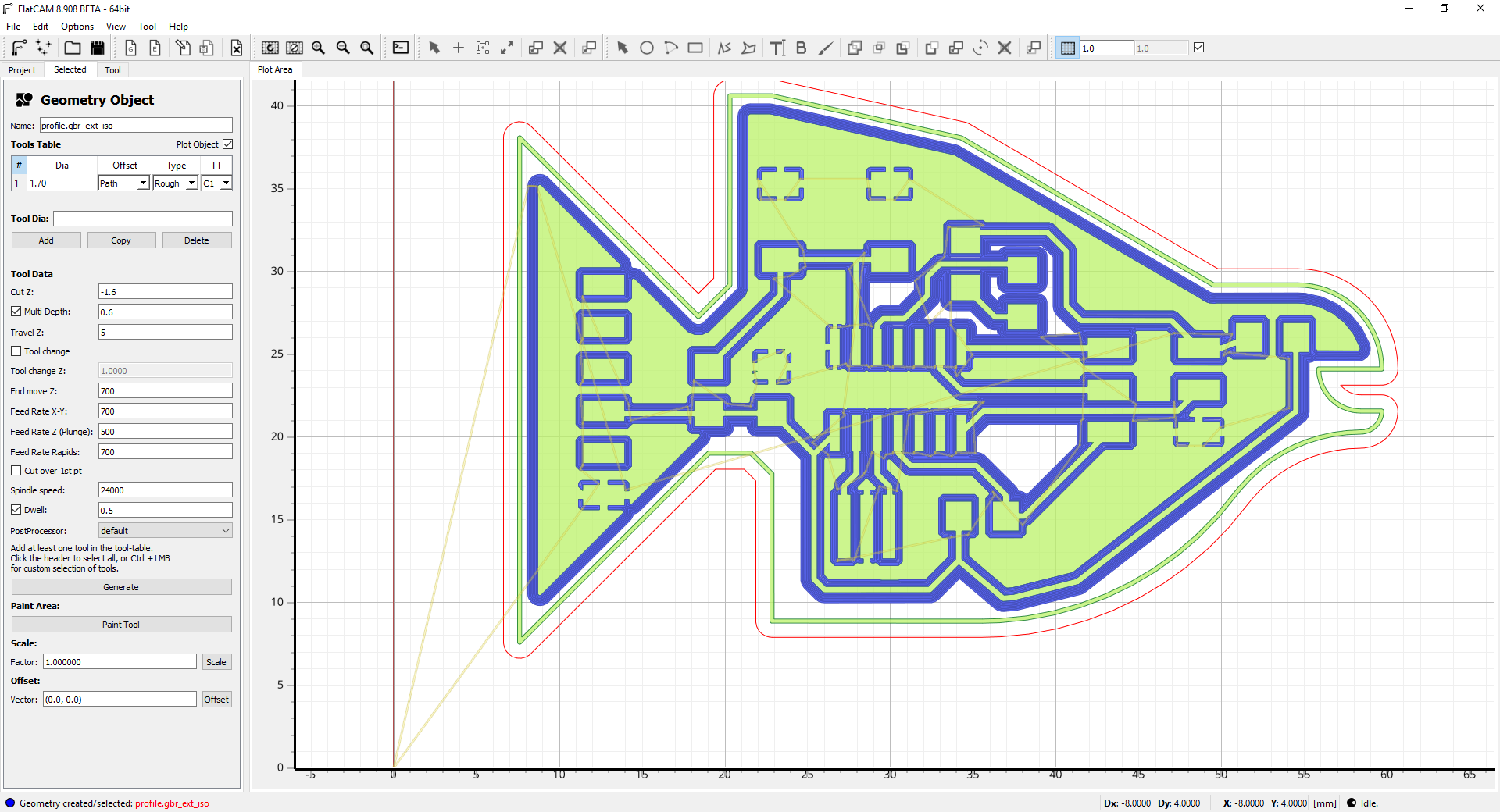
Now we generate the Gcode for the second part of the job.
Milling the board
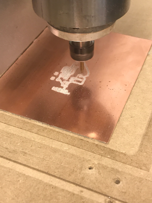
We are now ready to manufacture the board. To begin, we must put the first tool which is that of 1/64. It is important to check that the tool is straight and tight.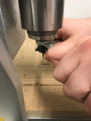
Thereafter, we must put the origin of the Z axis. This step is very critical because the copper layer of our PCB is very thin. So, if the origin is not perfect, we will go too deep in the PCB or not enough. A good way to do this is with a multimeter and a conductivity test. Just put a probe on the board and the other probe on the tool. It is necessary to go down slowly until a conduction occurs. I suggest 1 mil steps for better accuracy.
Now, all that remains is to set the origin on the X and Y axis. This origin can be placed anywhere on the board. I suggest placing it in one corner to be able to make another PCB on the second part.
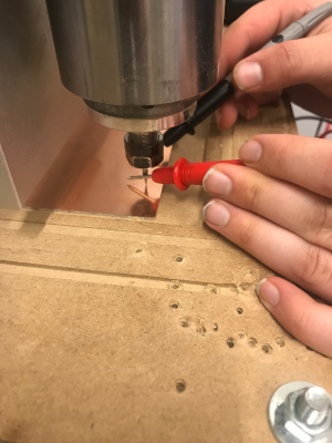
A photo during the process.
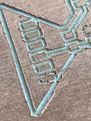
As you can see, the tool has been too deep in the board. This damaged the tracks of our circuit. The solution is to better stick the board to the platform of the CNC and also to originate the Z axis a little higher. We probably crush the tool on the board the first time we did the orgine.
During my second try, the controller of the cnc decided to break up. I had to wait to replace the controller of the CNC to be able to make my circuit again.
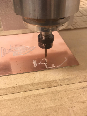
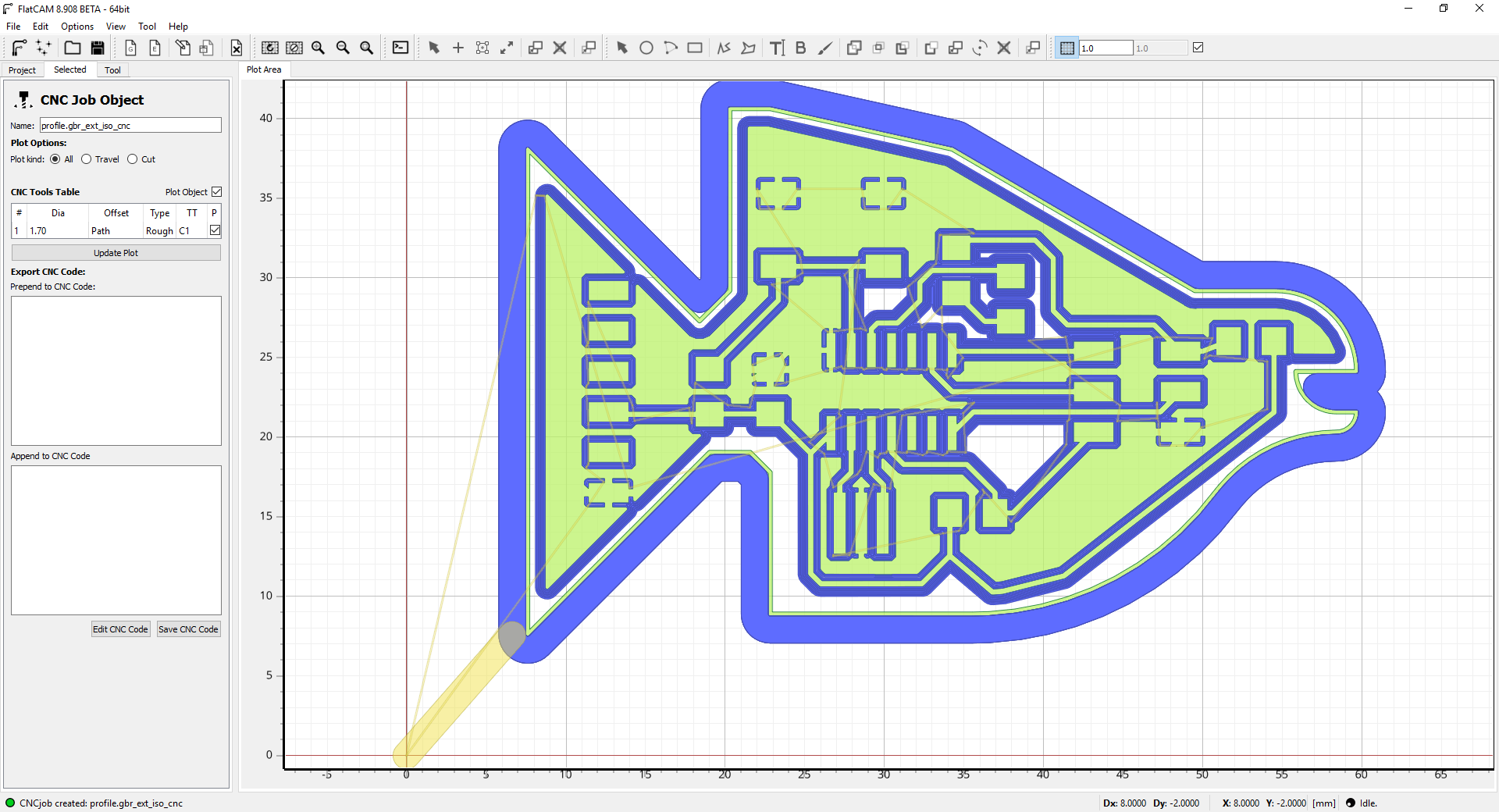
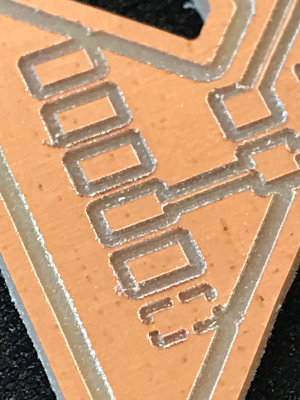
Here is the last milled circuit and you can see that the circuit tracks are much better. It can be seen that the CNC has been much less deep than the first one. Here is what a well-done milled circuit should look like.
Soldering the board
Here is my board after soldering all the components.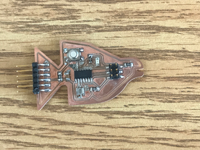
Group assignement
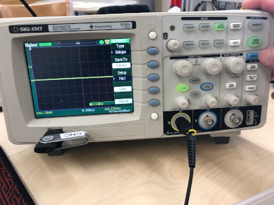
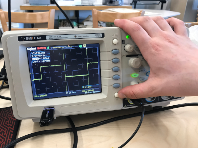
This week the person in charge of the assignment group is me. The group assignement is to use the test equipment in our lab to observe the operation of a microcontroller circuit board. I chose to use the oscilloscope to see the accuracy of microcontroller delays. The oscilloscope is a tool used to visualize the electrical signals of our circuit. Let's start by putting a program that flashes a led with a delay. I took the blink example provided with the arduino IDE and put a delay of 100 ms between blinking.Now you have to put the probe of the oscilloscope on the trace of the led to observe the signal. We notice that nothing happens on the oscilloscope. You have to adjust the image by pressing the auto button.
Now we can see the signal. It can also be observed that the signal moves between 0 and 5 volts. To measure the distance between two signals, it is possible to use the cursors button.
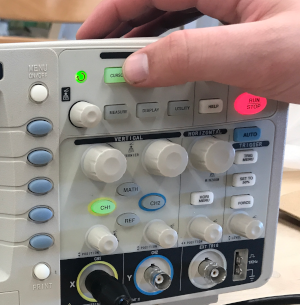
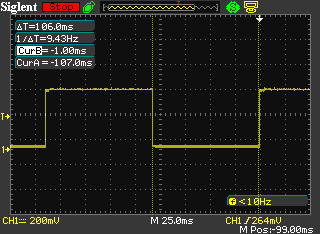
The cursor is moved with the wheel to superimpose them on the signal. It can be seen that the distance between the two courses is 106 ms. There is therefore a difference between the delay in the program and the actual delay.
Now, simply press the print button to save the oscilloscope image and put it on a flash drive.
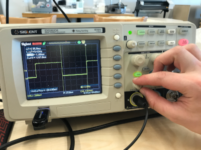
Here is the image taken with the oscilloscope and we see very clearly the 106 ms delay.
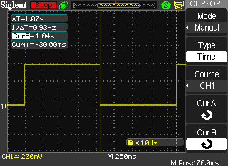
I wanted to do the same test again with a delay of 1 second. We can still see the actual delay is 1.07 seconds which is not exactly the delay in the program.
Here is an example of how to use an oscilloscope and what can be used to measure a signal. There are many other features to explore.
Hero shot
You can download all the files of this week right here.