Input Devices
This week our assignments are the following:
• Probe an input device's analog levels and digital signals (group)
• Measure something: add a sensor to a microcontroller board
that you have designed and read it (Individual)
Preparation
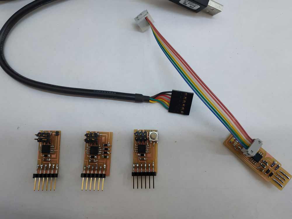
I decided to make push button, hall sensor and temperature sensors boards. My first step was to make a list of necessary components.
Introduction
Before starting assignement for this week I decided to learn what is input interfacing circuits.. An input device responds to changes in the environment and produces a suitable electrical signal for processing in an electronic circuit. In all input devices, other forms of energy are transformed into electrical energy. Here are some common input devices with examples of how they can be used.• Photo-voltaic cell- produces a voltage when light falls on it, provides energy for satellites.
• Capacitor - used in timing circuits and electronic amplifiers.
• Switch - allows current in a circuit when closed.
• Voltage divider - To create a voltage across the bottom component that can then be sent to a process device. Used in devices, f eg npn transistors, where a voltage change switches on or off a circuit.
• Resistor - used in circuits to set current. Input Interfacing allows sensors to communicate with PCs and microcontrollers. For an electronic circuit to be useful and effective, it has to interface with something. Input interface circuits connect electronic circuits such as op-amps, logic gates... to the outside world expanding its capabilities. Electronic circuits amplify, buffer or process signals from sensors or switches as input information or to control relays or actuators for output control.Input interfacing circuits convert the voltage and current output of one circuit to the equivalent of another. Input sensors provide an input for information about an environment. For example thermistors, magnetic sensors, switches... All these devices are categorized as input devices.
What I need to do for this assignement
• Learn how the input devices works, how the boards work etc.• Prepare all tools, components, materials and machines.
• Download the boards and prepare them for cutting.
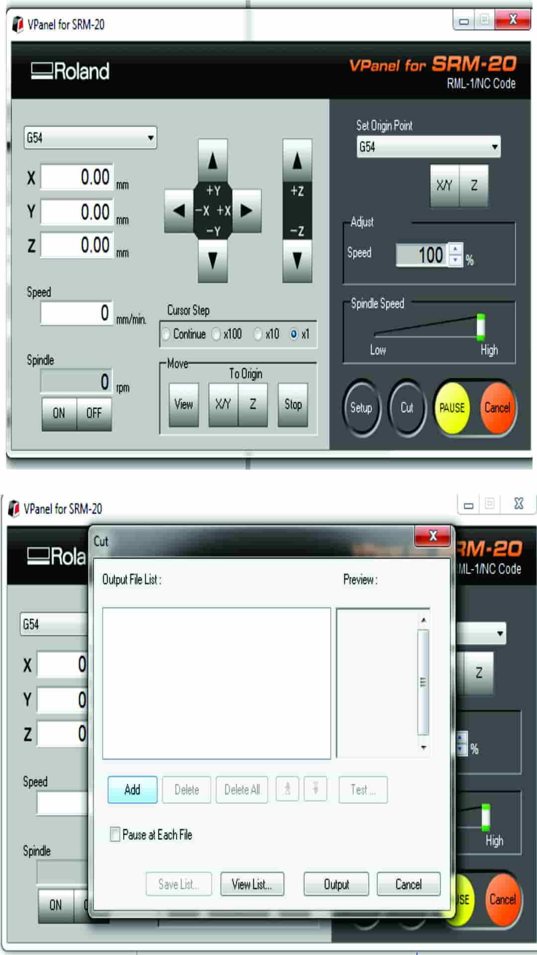
• Set - up the machien (SRM-20).
• Cut the boards.
• Solder the components.
• Check the if all components soldered properly.
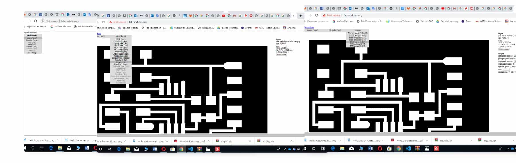
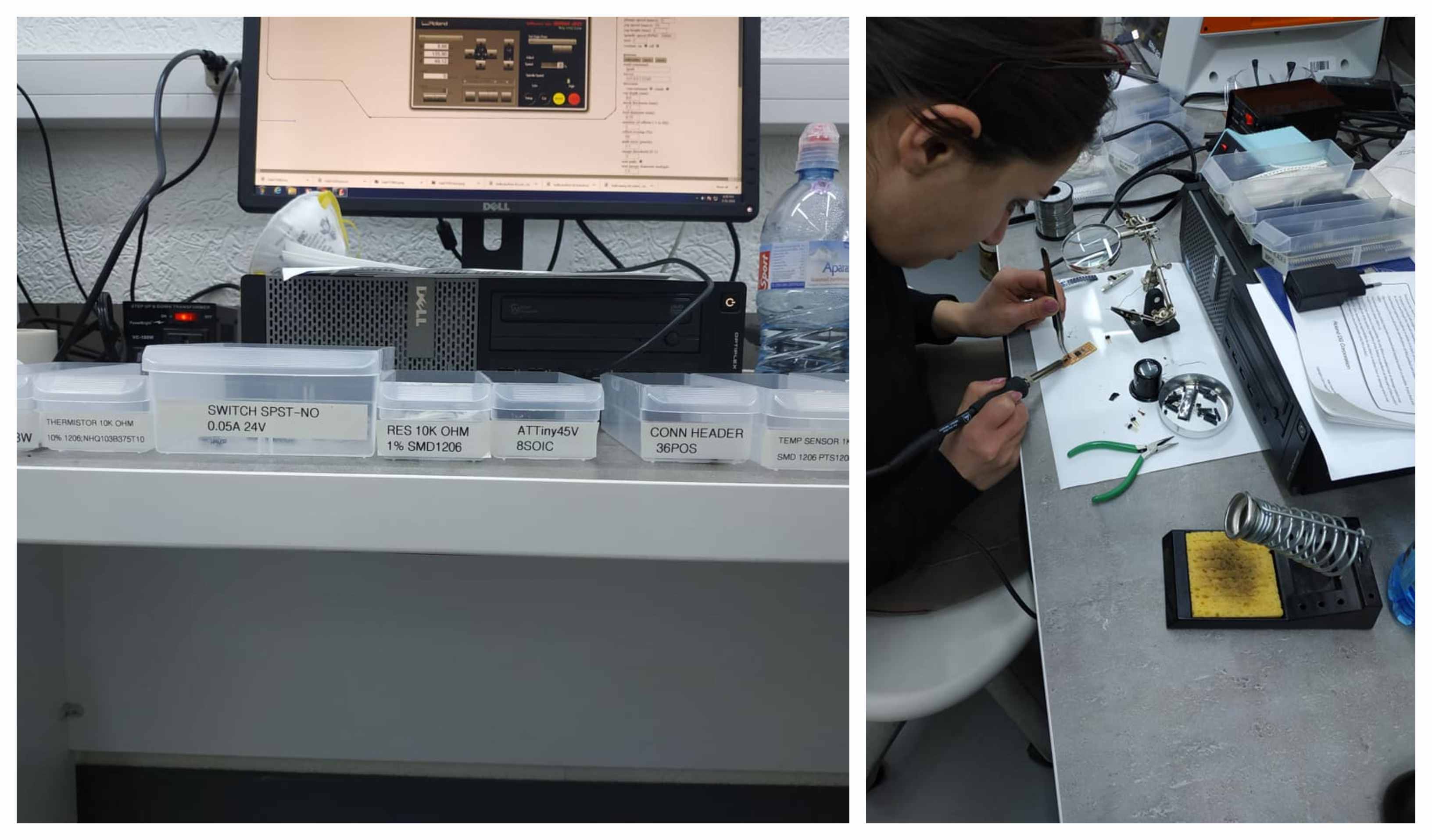
• Programming and testing. When I took all componets I downloaded all png files, opened fab mudules and started preparing files for cutting.
Setting up the machine
• Turn on the machine
• Put the material in the machine, fixed it with double sided stick
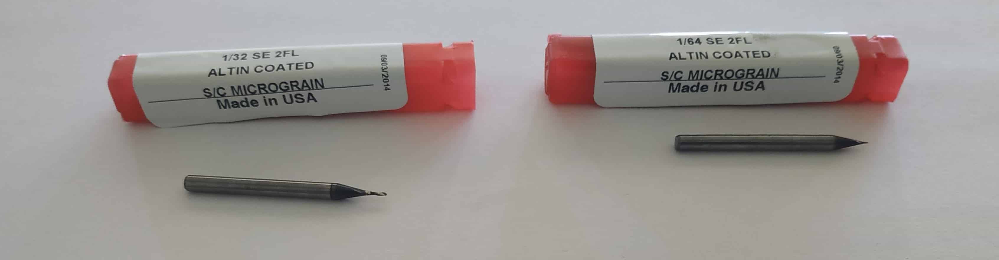
• Attached end mill 1/64 for milling traces
• Opened fab modules and upload my files there, then saved
• Setted the origin point chose"[Machine Coordinate System" in our case will use "G54" and "G55" that's the first 2 of 6 Work Coordinate Systems. During this process I used Vpanel pointers "right" "left" "up" "down"
Picture of endmills I used
• Went back to fab modules and chose image "png"- Gcode "nc"-PCB traces "1/64" - "selected calculate" - "save". When the files had been saved I sent them to machine for cutting. Started the cutting process and paused to check how it was going on. After I continued the cutting. I repeated above mentioned activities 3 times for all boards. For cutting out the boards I opened fab modules chose image "png"- Gcode "nc"-PCB interior "1/32" - "selected calculate" - "save". Then I cleaned all boards and started soldering process.
Board for the measurment of magnetic field
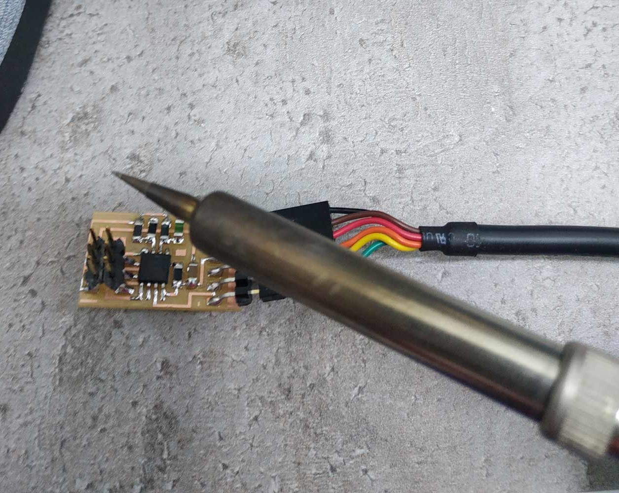
Soldering
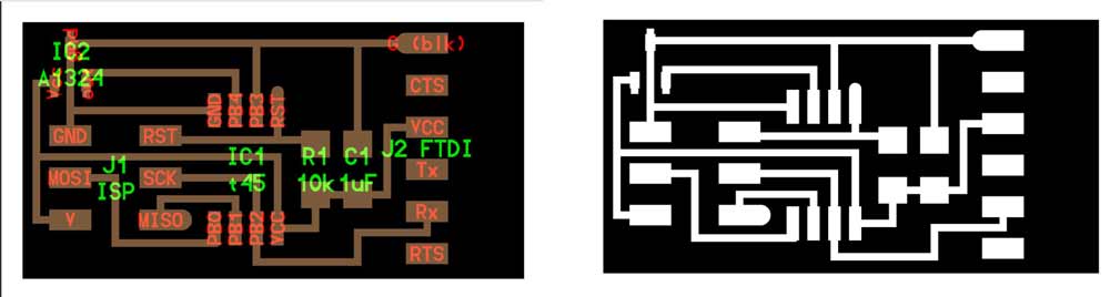
For soldering I used Weller soldering station,I soldered the components with 350 degree of Celsius. I used the following electronics componentsATtiny45 is the microcontroller, which are used. More detailed it will be described later. ATtiny45 is high-performance, low-power Microchip 8-bit AVR RISC-based microcontroller combines 4KB ISP flash memory, 256-Byte EEPROM, 256B SRAM, 6 general purpose I/O lines, 32 general \purpose working registers, one 8-bit timer/counter with compare modes, one 8-bit high speed timer/counter, USI, internal and external Interrupts, 4-channel 10-bit A/D converter, programmable watchdog timer with internal oscillator, three software selectable power saving modes, and debugWIRE for on-chip debugging. The device achieves a throughput of 20 MIPS at 20 MHz and operates between 2.7-5.5 volts. By executing powerful instructions in a single clock cycle, the device achieves throughputs approaching 1 MIPS per MHz, balancing power consumption and processing speed.
Hall sensor board
• ATtiny 45 microcontroller
• 10k SMD 1206 resistor
• 1uF SMD 1206 capacitor
• Hall effect sensor
• 1x6 male pin headers
• 2x3 male pin headers
Temperature sensor booard
• ATtiny 45 microcontroller
• 10k SMD 1206 resistor
• 1uF SMD 1206 capacitor
• Temperature sensor
• 1x6 male pin headers
• 2x3 male pin headers
Switch/button board
• ATtiny 45 microcontroller
• 10k SMD 1206 resistor
• 1uF SMD 1206 capacitor
• B3SN-3112P push button
• 1x6 male pin headers
• 2x3 male pin headers
Magnetic field
Magnetic sensor converts magnetic infromation into electrical signals for processing by electronic circuits. These sensors are designed to respond to a wide range of positive and negative magnetic fields in a variety of different applications and 1 type of magnet sensor whose output signal is a function of magnetic field density around it is called the "hall effect sensor". Hall effect sensors are devices which are activated by an external magnetic field. Magnetic field has 2 important characteristics flux density, (B) and polarity (North and South Poles). The output signal from the sensor is the function of magnetic field density around the device. When the magnetic flux density around the sensor exceeds a certain pre-set range, the sensor detects it and generates an output voltage called the "hall voltage". When the device is placed within a magnetic field, the magnetic flux lines exert a force on the semiconductor material which deflects the charge carriers, electrons and holes, to either side of the semiconductor slab. This movement of charge carriers is a result of the magnetic force they experience passing through the semiconductor material. There are 2 basic types of digital hall effect sensor, bipolar and unipolar. Bipolar sensor require a positive magnetic field (south pole) to operate them and a negative field (north pole) to release them while unipolar sensors require only a single magnetic south pole to both operate and release them as they move in and out of the magnetic field.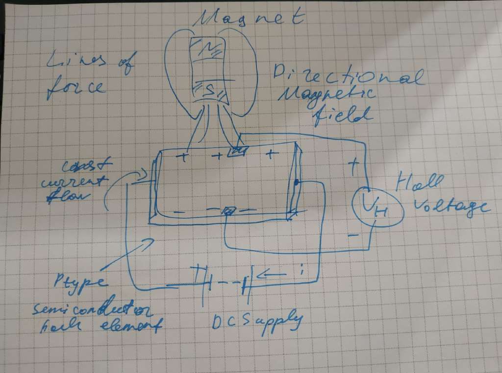
As these electrons and holes move side wards a potential difference is produced between the 2 sides of the semiconductor material by the build-up of these charge carriers. Then the movement of electrons through the semiconductor material is affected by the presence of an external magnetic field which is at right angles to it and this effect is greater in a flat rectangular shaped material. To generate a potential difference across the device the magnetic flux lines must be perpendicular, 90 degree to the flow of current and be of the correct polarity, generally a south pole. Hall effect provides information regarding the type of magnetic pole and magnitude of the magnetic field. These sensors are available with either analogue or digital outputs. The output signal for analogue sensors is taken directly from the output of the operational amplifier with the output voltage being directly proportional to the magnetic field passing through the hall sensor. Analogue sensor gives a continuous voltage output that increases with a strong magnetic field and decreases with a weak magnetic field. Output hall effect sensors, as the strength of the magnetic field increases the output signal from the amplifier will also increase until it begins to saturate by the limits imposed on it by the power supply. Any additional increase in the magnetic field will have no effect on the output but drive it more into saturation. Digital output sensors on the other hand have a Schmitt trigger with built in hysteresis connected to the op-amp. When the magnetic flux passing through the hall sensor exceeds a pre-set value the output from the device switches quickly between its “off” condition to an “on” condition without any type of contact bounce. This built in hysteresis eliminates any oscillation of the output signal as the sensor moves in and out of the magnetic field. Then digital output sensors have just 2 states, “on” and “off”.
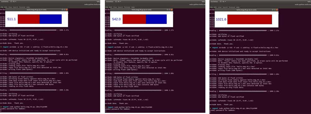
I connected Fab ISP to the board, then FTDI cable connected to the same board and connected them to the computer by USB port. The board has 6 pins for connecting fab ISP and 6 pins FTDI. Opened "Hall sensor folder" by right clicked Open In terminal and typed the command
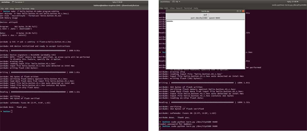
"make -f hello.mag.45.make program-usbtiny" "make -f hello.mag.45.make program-usbtiny" and pressed enter. "program-usbtiny" specifies the programmer we're going to use change "usbtiny" to "avrisp2" or "dragon_isp" in case of we used that programmers.
After typed "avrdude -p t45 -P usb -c usbtiny -U flash:w:hello.mag.45.c.hex"" command end pressed enter and then typed "sudo python hello.mag.45.py /dev/ttyUSB0 9600"command.
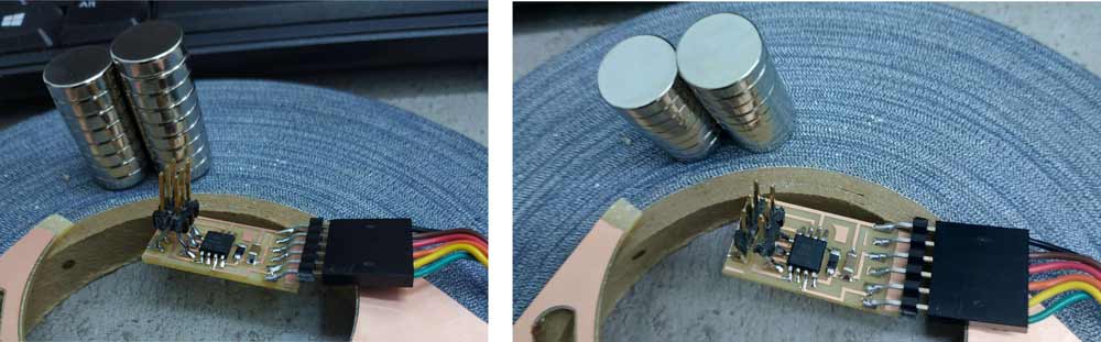
After the programming I used magnets for measuring the magnetic field.
As I used FTDI, I changed the /ttyUSB0 to /ttyACM0
Temperature sensor
A thermistor is a resistor that changes in value according to it’s heat. In actual fact all
resistors change in value as they heat up or cool down, but thermistors are
manufactured to show a large resistance change. Connecting the thermistor to the
microcontroller is very straight forward, but some software "calibrating" is required.
Note that the thermistor response is not analogue, and so the readings will not change.
In general there is a larger resistance change at lower temperatures. This can be
compensated for in the software by using a smaller range at higher temperatures.
Temperature sensors measure the amount of heat energy generated by an object or system,
allowing us to detect any physical change to that temperature producing either an analog
or digital output.
There are different types of temperature sensors. I will write about RTD (Resistance
Temperature Probe)
and NTC(Negative Temperature Coefficient). RTD made of Platinum metal which has a resistance
value of 100 ohms
at zero degrees Celsius.
NTC is a type of thermistor, which have resistance that decreases with increasing
temperature.
Both RTD and NTC require a current or excitation source, and both are suitable for use in
applications that require
•accuracy
•good long-term stability
•immunity to electrical noise in the environment
The main difference between thermistors and RTD is the temperature range. If your
application involves
temperatures above 130°C, the RTD is your only option.
Below that temperature, NTC are often preferred when accuracy is important. RTD, on the
other hand,
are chosen when tolerance is important.
NTC are better for precision measurement and RTD for temperature compensation.
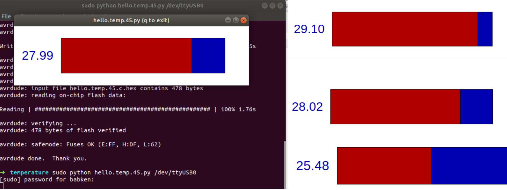
After cutting and soldering the board
I tested it using tester and found out
that I did not solder all components
properly and desoldered some components and soldered them again.
The board has 6 pins for connecting fab ISP and 6 pins FTDI.
The final attempt was succesful and the board was ready for programming.
Connected Fab ISP and FTDI cable to the board then all them connected to the computer by USB
port
and opened the tepmerature folder by right click selected open in terminal function.
Typed the following commands
• "make -f hello.temp.45.make program-usbtiny" "program-usbtiny" specifies the
programmer we're going to use change
"usbtiny" to "avrisp2" or "dragon_isp" in case of we used that programmers
• "avrdude -p t45 -P usb -c usbtiny -U flash:w:hello.temp.45.c.hex"
• "sudo python hello.temp.45.py /dev/ttyUSB0 9600"
As I used FTDI, I changed the /ttyUSB0 to /ttyACM0
Finnaly my programm started work and I start testing the board.
I used soldering iron for measuring temperature.
Switch/button
There are a large variety of switches available, but the majority all have 2 "contacts" which are either "open" (off) or "closed" (on). All switches/buttons "jump" when the switch/button opens or closes. It means that the switch/button contacts "jump" against each other before settling. As the microcontroller operates so quickly it is possible that in some programs the microcontroller may register 2 or 3 of these "jumps" instead of just registering one "push".I cut the board, soldered the components.
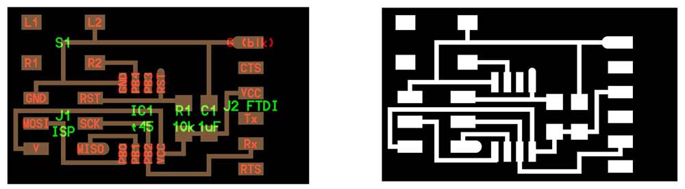
The board has 6 pins for connecting fab ISP and 6 pins FTDI.
Started programming process, connected FAB ISP and FTDI cable to the board after to the computer, opened the folder by right click
"open in terminal"
and start typing
• "make -f hello.button.45.make program-usbtiny" "program-usbtiny" specifies the
programmer we're going
to use change "usbtiny" to "avrisp2" or "dragon_isp" in case of we used that programmers
• typed the command and hit enter "avrdude -p t45 -P usb -c usbtiny -U
flash:w:hello.button.45.c.hex"
• installed python's serial module for reading data through FTDI cable "sudo apt install
python-serial"
• "ls /dev" and found "ttyUSB0"
• "sudo python term.py /dev/ttyUSB0 9600"
I changed the (du) into (ku)
Programming/code
When the board was ready I started programing it and had some problems with Windows 10 and
decided to use
another computer with Linux (Babken's computer). For programing the board I needed "C"
codes, makefiles and python program to read the data from the keynotes for single board. I created separate
folders for them "Nutton folder", "Hall sensor folder" "Temperature sensor folder".
I also need Fab ISP and FTDI Cable for this assignment.
Fab ISP (In system programmer) is designed in fab lab and it is another version of an AVR
programmer.
It helps me to program the microcontrollers on other boards I made, using a USB cable and
6-pin IDC to 6-pin IDC cable.
About Fab ISP you can read at week5
The FTDI cable is a USB to Serial (TTL level) converter which allows for a simple way
to connect TTL interface devices to USB. The I/O pins of this FTDI cable are configured to
operate at 5V.
The FTDI cable develops, manufactures, and supports devices and their related software
drivers for converting RS-232 or
TTL serial transmissions to USB signals, in order to allow support for legacy devices with
modern computers.
FTDI provides application-specific integrated circuit (ASIC) design services.
They also provide consultancy services for product design, specifically in the real of
electronic devices.
Before starting the programming process I started reading
ATtiny 45 microcontroller's datasheet.
I will try to write about some important parts of the microcontroller.
.jpg)
Here I will describe the pins
• VCC - supply voltage
• GND - ground
• Port B (PB5:PB0) - Port B is a 6-bit bi-directional I/O port with internal pull-up resistors
(selected for each bit). The Port B output buffers have symmetrical drive characteristics with both
high sink and source capability. As inputs, Port B pins that are externally pulled low will source
current, if the pull-up resistors are activated. The Port B pins are tri-stated, when a
reset condition becomes active, even if the clock is not running.
• "RESET" - Reset input. A low level on this pin for longer than the minimum pulse length will generate
a reset, even if the clock is not running and provided the reset pin has not been disabled.
Reset input. A low level on this pin for longer than the minimum pulse length will generate a reset, even if
the clock isn't running and provided the reset pin has not been disabled. Below you can see
the minimum pulse length
.jpg)
Here I wrote some information (which were usefull for me) about noise cancelation, analog to digital Converter, etc. More detailed information
you can read in ATtiny45 datasheet.
ATtiny45 is a low power CMOS 8-bit microcontroller based on the AVR enhanced RISC architecture. By
executing powerful instructions in a single clock cycle, the microcontroller achieves throughputs approaching 1
MIPS per MHz allowing the system designer to optimize power consumption versus processing speed.
The ATtiny45 features a 10-bit successive approximation analog to digital Converter (ADC). The ADC is
connected to a 4-channel analog multiplexer which allows one differential voltage input and 4 single-ended voltage
inputs constructed from the pins of Port B. The differential input (PB3, PB4 or PB2, PB5) is equipped with a
programmable gain stage, providing amplification step of 26 dB (20x) on the differential input voltage before the
A/D conversion. The single-ended voltage inputs refer to 0V (GND).
ADC contains a sample and Hold circuit which ensures that the input voltage to the ADC is held at a constant
level during conversion. A block diagram of the ADC.
The ADC converts an analog input voltage to a 10-bit digital value through successive approximation. The minimum value represents
GND and the maximum value represents the voltage on VCC, the voltage on the AREF pin
or an internal 1.1V / 2.56V voltage reference.
The voltage reference for the ADC may be selected by writing to the REFS[2:0] bits in ADMUX. The VCC supply,
the AREF pin or an internal 1.1V / 2.56V voltage reference may be selected as the ADC voltage reference. Optionally the internal
2.56V voltage reference may be decoupled by an external capacitor at the AREF pin to improve
noise immunity.
The analog input channel and differential gain are selected by writing to the MUX[3:0] bits in ADMUX. Any of the
four ADC input pins ADC[3:0] can be selected as single ended inputs to the ADC. ADC2 or ADC0 can be selected
as positive input and ADC0, ADC1, ADC2 or ADC3 can be selected as negative input to the differential gain
amplifier.
If differential channels are selected, the differential gain stage amplifies the voltage difference between the
selected input pair by the selected gain factor, 1x or 20x, according to the setting of the MUX[3:0] bits in ADMUX.
This amplified value then becomes the analog input to the ADC. If single ended channels are used, the gain amplifier is bypassed altogether.
For example the temperature sensor or Hall effect sensor is selected by writing the code “1111” to the MUX[3:0] bits in ADMUX register
when the ADC4 channel is used as an ADC input.
The ADC is enabled by setting the ADC Enable bit, ADEN in ADCSRA. Voltage reference and input channel selections will not go into effect until ADEN is set.
The ADC does not consume power when ADEN is cleared, so it is
recommended to switch off the ADC before entering power saving sleep modes.
The ADC generates a 10-bit result which is presented in the ADC Data Registers, ADCH and ADCL. By default,
the result is presented right adjusted, but can optionally be presented left adjusted by setting the ADLAR bit in
ADMUX.
A single conversion is started by writing a logical one to the ADC start conversion bit, ADSC. This bit stays high as
long as the conversion is in progress and will be cleared by hardware when the conversion is completed.
If a different data channel is selected while a conversion is in progress, the ADC will finish the current conversion
before performing the channel change.
The ADC features a noise canceler that enables conversion during sleep mode to reduce noise induced from the
CPU core and other I/O peripherals. The noise canceler can be used with ADC Noise Reduction and Idle mode.
To make use of this feature, the following procedure should be used:
• Make sure that the ADC is enabled and is not busy converting. Single Conversion mode must be selected and
the ADC conversion complete interrupt must be enabled.
• Enter ADC Noise Reduction mode (or Idle mode). The ADC will start a conversion once the CPU has been
halted.
• If no other interrupts occur before the ADC conversion completes, the ADC interrupt will wake up the CPU and
execute the ADC Conversion Complete interrupt routine. If another interrupt wakes up the CPU before the ADC
conversion is complete, that interrupt will be executed, and an ADC Conversion Complete interrupt request will
be generated when the ADC conversion completes. The CPU will remain in active mode until a new sleep
command is executed.
Noise Canceling Techniques
Digital circuitry inside and outside the device generates EMI which might affect the accuracy of analog measurements.
If conversion accuracy is critical, the noise level can be reduced by applying the following techniques:
• Keep analog signal paths as short as possible.
• Make sure analog tracks run over the analog ground plane.
• Keep analog tracks well away from high-speed switching digital tracks.
• If any port pin is used as a digital output, it mustn’t switch while a conversion is in progress.
• Place by pass capacitors as close to VCC and GND pins as possible.
Example - Temperature Measurement
The temperature measurement is based on an temperature sensor that is coupled to a single ended ADC4
channel. Selecting the ADC4 channel by writing the MUX[3:0] bits in ADMUX register to “1111” enables the
temperature sensor.
The internal 1.1V reference must also be selected for the ADC reference source in the
temperature sensor measurement. When the temperature sensor is enabled, the ADC converter can be used in
single conversion mode to measure the voltage over the temperature sensor.
The measured voltage has a linear relationship to the temperature as described in the picture below. The sensitivity is
approximately 1 LSB / degree celcius (C) and the accuracy depends on the method of user calibration. Typically, the measurement
accuracy after a single temperature calibration is ±10degree celcius (C),
assuming calibration at room temperature. Better accuracies are achieved by using two temperature points for calibration.

The values described in table are typical values. Due to process variation the temperature sensor
output voltage varies from one chip to another. To be capable of achieving more accurate results the temperature
measurement can be calibrated in the application software.
The sofware calibration can be done using the formula:
>

Where ADCH and ADCL are the ADC data registers, "k" is the fixed slope coefficient and T(os) is the temperature sensor offset.
Typically, k is very close to 1.0 and in single-point calibration the coefficient may be omitted. Where
higher accuracy is required the slope coefficient should be evaluated based on measurements at 2
temperatures.
More detailed information about the ADMUX – ADC Multiplexer Selection Register and ADCL and ADCH – The ADC Data Register
in the datasheet on the pages 133-138.
Now I will try to explain the codes
"#define" is a C preprocessor directive used to define macros. A preprocessor directive is a program statement which is invoked before the
program compilation takes place.
In programming, when "void" is used as a function return type, it indicates that the function does not return a value. When void appears
in a pointer declaration, it specifies that the pointer is universal. When used in a function's parameter list, void indicates that the
function takes no parameters.
"Void" functions, also called nonvalue-returning functions, are used just like value-returning functions except void return types do
not return a value when the function is executed.
The void function accomplishes its task and then returns control to the caller.
The void function call is a stand-alone statement.
"While (1)" is is a forever loop.
ADMUX = (0 << REFS2) | (0 << REFS1) | (0 << REFS0) // VCC ref
| (0 << ADLAR) // right adjust
| (0 << MUX3) | (1 << MUX2) | (1 << MUX1) | (1 << MUX0); // 20(PB4-PB3)
ADCSRA = (1 << ADEN) // enable
| (1 << ADPS2) | (1 << ADPS1) | (1 << ADPS0); // prescaler /128
ADCSRB = (1 << BIN); // bipolar mode
//
ADMUX (ADC multiplexer selection register) is used to select the analog port channel to be used, voltage reference for the
ADC operation and the data presentation of the ADC result in the ADCL and ADCH data registers after conversion.
"ADMUX" is defined in the compiler header files that get included.identifies which -channel- of the "MUX" we want to use.
The "channel" corresponds to the pin we want to use.
Our micricontroller has multi-purpose pins. This means we can use them for one thing or another.
If we say "ADMUX = 0", we are choosing channel 0 ( pin ADC0) and telling the ADC to watch that pin for an analog voltage level.
Once it registers that voltage level,
it converts that to an 8-it digital value, which is what we get when we combine and read the high and low ADC registers.
We leave "REFS1", "REFS2" and "REFS0" to it is default value (logical "0") which means we use the external voltage reference.
The "ADLAR" bit is set to logical "0".
• (0 << REFS2) output is 0
• (0 << REFS1) output is 0
• (0 << REFS0) output is 0
The ADLAR bit is set to logical "0", which means we instruct the microcontroller to place the highest
bits data conversion in "ADLR" and the lowest 8 bits data conversion in ADLC register.
The "MUX3", "MUX2", "MUX1" and "MUX0" bits is the analog input port selector.
ADCSRA (Control Status and Status Register) - the function of this register is to control the microcontroller
ADC operation such as enabling the ADC feature, start converting, prescaler selection and interrupt control.
This code sets the ADEN bit therefore the "ADCSRA" register will have "ADEN=1" value.
The "ADPS2", "ADPS1" and "ADPS0" bits are used to set the circuit clock prescaler.
This code will set the "ADEN", "ADPS2", "ADPS0" and "ADPS1" bits.
// main loop
//
while (1) {
//
// accumulate samples
//
accum = 0;
for (count = 0; count < nsamples; ++count) {
//
// initiate conversion
//
ADCSRA |= (1 << ADSC);
//
// wait for completion
//
while (ADCSRA & (1 << ADSC))
;
//
//
accum += ADC;
}
//
// send framing
"While(1)" is a forever loop. It means that the process will last as long as it receives
voltage/electricity.
//
put_char(&serial_port, serial_pin_out, 1);
char_delay();
put_char(&serial_port, serial_pin_out, 2);
char_delay();
put_char(&serial_port, serial_pin_out, 3);
char_delay();
put_char(&serial_port, serial_pin_out, 4);
char_delay();
//
// send result
//
put_char(&serial_port, serial_pin_out, (accum & 255));
char_delay();
put_char(&serial_port, serial_pin_out, ((accum >> 8) & 255));
char_delay();
put_char(&serial_port, serial_pin_out, ((accum >> 16) & 255));
char_delay();
}
}
Such we are display the numbers on the screen.
The conclusion is, that we should transform analog signal into digital. When the sensor produce
voltage we transform it into digital signal and display it on the screen. Transform it into 8 bit digital value.
and print it on the desctop.
// main loop
//
while (1) {
//
// wait for button down
//
while (0 != pin_test(input_pins,input_pin))
;
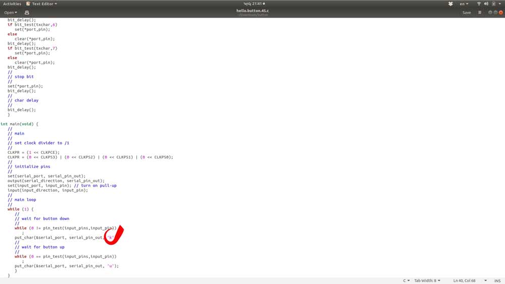
put_char(&serial_port, serial_pin_out, 'k');
//
// wait for button up
//
while (0 == pin_test(input_pins,input_pin))
;
put_char(&serial_port, serial_pin_out, 'u');
}
}
In this part when the button is pushed it displays "k" and otherwise "u"
This process lasts as long as we repeat the action.
Code
Magnetic field mesuring board code. I have used Neils code to program my board.
		//
		// hello.mag.45.c
		//
		// Hall effect magnetic sensing hello-world
		//    9600 baud FTDI interface
		//
		// Neil Gershenfeld 11/3/13
		// (c) Massachusetts Institute of Technology 2013
		//
		// This work may be reproduced, modified, distributed,
		// performed, and displayed for any purpose. Copyright is
		// retained and must be preserved. The work is provided
		// as is; no warranty is provided, and users accept all
		// liability.
		//

		#include
		#include

		#define output(directions,pin) (directions |= pin) // set port direction for output
		#define set(port,pin) (port |= pin) // set port pin
		#define clear(port,pin) (port &= (~pin)) // clear port pin
		#define pin_test(pins,pin) (pins & pin) // test for port pin
		#define bit_test(byte,bit) (byte & (1 << bit)) // test for bit set
		#define bit_delay_time 102 // bit delay for 9600 with overhead
		#define bit_delay() _delay_us(bit_delay_time) // RS232 bit delay
		#define half_bit_delay() _delay_us(bit_delay_time/2) // RS232 half bit delay
		#define char_delay() _delay_ms(10) // char delay

		#define serial_port PORTB
		#define serial_direction DDRB
		#define serial_pin_out (1 << PB2)

		#define nsamples 100 // number of samples to accumulate

		void put_char(volatile unsigned char *port, unsigned char pin, char txchar) {
		   //
		   // send character in txchar on port pin
		   //    assumes line driver (inverts bits)
		   //
		   // start bit
		   //
		   clear(*port,pin);
		   bit_delay();
		   //
		   // unrolled loop to write data bits
		   //
		   if bit_test(txchar,0)
			  set(*port,pin);
		   else
			  clear(*port,pin);
		   bit_delay();
		   if bit_test(txchar,1)
			  set(*port,pin);
		   else
			  clear(*port,pin);
		   bit_delay();
		   if bit_test(txchar,2)
			  set(*port,pin);
		   else
			  clear(*port,pin);
		   bit_delay();
		   if bit_test(txchar,3)
			  set(*port,pin);
		   else
			  clear(*port,pin);
		   bit_delay();
		   if bit_test(txchar,4)
			  set(*port,pin);
		   else
			  clear(*port,pin);
		   bit_delay();
		   if bit_test(txchar,5)
			  set(*port,pin);
		   else
			  clear(*port,pin);
		   bit_delay();
		   if bit_test(txchar,6)
			  set(*port,pin);
		   else
			  clear(*port,pin);
		   bit_delay();
		   if bit_test(txchar,7)
			  set(*port,pin);
		   else
			  clear(*port,pin);
		   bit_delay();
		   //
		   // stop bit
		   //
		   set(*port,pin);
		   bit_delay();
		   //
		   // char delay
		   //
		   bit_delay();
		   }

		int main(void) {
		   //
		   // main
		   //
		   static uint16_t count;
		   static uint32_t accum;
		   //
		   // set clock divider to /1
		   //
		   CLKPR = (1 << CLKPCE);
		   CLKPR = (0 << CLKPS3) | (0 << CLKPS2) | (0 << CLKPS1) | (0 << CLKPS0);
		   //
		   // initialize output pins
		   //
		   set(serial_port, serial_pin_out);
		   output(serial_direction, serial_pin_out);
		   //
		   // init A/D
		   //
		   ADMUX = (0 << REFS2) | (0 << REFS1) | (0 << REFS0) // Vcc ref
			  | (0 << ADLAR) // right adjust
			  | (0 << MUX3) | (0 << MUX2) | (1 << MUX1) | (0 << MUX0); // ADC4
		   ADCSRA = (1 << ADEN) // enable
			  | (1 << ADPS2) | (1 << ADPS1) | (1 << ADPS0); // prescaler /128
		   //
		   // main loop
		   //
		   while (1) {
			  //
			  // accumulate samples
			  //
			  accum = 0;
			  for (count = 0; count < nsamples; ++count) {
				 //
				 // initiate conversion
				 //
				 ADCSRA |= (1 << ADSC);
				 //
				 // wait for completion
				 //
				 while (ADCSRA & (1 << ADSC))
					;
				 //
				 // add result
				 //
				 accum += ADC;
				 }
			  //
			  // send framing
			  //
			  put_char(&serial_port, serial_pin_out, 1);
			  char_delay();
			  put_char(&serial_port, serial_pin_out, 2);
			  char_delay();
			  put_char(&serial_port, serial_pin_out, 3);
			  char_delay();
			  put_char(&serial_port, serial_pin_out, 4);
			  char_delay();
			  //
			  // send result
			  //
			  put_char(&serial_port, serial_pin_out, (accum & 255));
			  char_delay();
			  put_char(&serial_port, serial_pin_out, ((accum >> 8) & 255));
			  char_delay();
			  put_char(&serial_port, serial_pin_out, ((accum >> 16) & 255));
			  char_delay();
			  }
		   }
Temperature mesuring board code
		//
		//
		// hello.temp.45.c
		//
		// thermistor hello-world
		//    9600 baud FTDI interface
		//
		// Neil Gershenfeld
		// 10/27/10
		//
		// (c) Massachusetts Institute of Technology 2010
		// This work may be reproduced, modified, distributed,
		// performed, and displayed for any purpose. Copyright is
		// retained and must be preserved. The work is provided
		// as is; no warranty is provided, and users accept all
		// liability.
		//

		#include
		#include

		#define output(directions,pin) (directions |= pin) // set port direction for output
		#define set(port,pin) (port |= pin) // set port pin
		#define clear(port,pin) (port &= (~pin)) // clear port pin
		#define pin_test(pins,pin) (pins & pin) // test for port pin
		#define bit_test(byte,bit) (byte & (1 << bit)) // test for bit set
		#define bit_delay_time 102 // bit delay for 9600 with overhead
		#define bit_delay() _delay_us(bit_delay_time) // RS232 bit delay
		#define half_bit_delay() _delay_us(bit_delay_time/2) // RS232 half bit delay
		#define char_delay() _delay_ms(10) // char delay

		#define serial_port PORTB
		#define serial_direction DDRB
		#define serial_pin_out (1 << PB2)

		void put_char(volatile unsigned char *port, unsigned char pin, char txchar) {
		   //
		   // send character in txchar on port pin
		   //    assumes line driver (inverts bits)
		   //
		   // start bit
		   //
		   clear(*port,pin);
		   bit_delay();
		   //
		   // unrolled loop to write data bits
		   //
		   if bit_test(txchar,0)
			  set(*port,pin);
		   else
			  clear(*port,pin);
		   bit_delay();
		   if bit_test(txchar,1)
			  set(*port,pin);
		   else
			  clear(*port,pin);
		   bit_delay();
		   if bit_test(txchar,2)
			  set(*port,pin);
		   else
			  clear(*port,pin);
		   bit_delay();
		   if bit_test(txchar,3)
			  set(*port,pin);
		   else
			  clear(*port,pin);
		   bit_delay();
		   if bit_test(txchar,4)
			  set(*port,pin);
		   else
			  clear(*port,pin);
		   bit_delay();
		   if bit_test(txchar,5)
			  set(*port,pin);
		   else
			  clear(*port,pin);
		   bit_delay();
		   if bit_test(txchar,6)
			  set(*port,pin);
		   else
			  clear(*port,pin);
		   bit_delay();
		   if bit_test(txchar,7)
			  set(*port,pin);
		   else
			  clear(*port,pin);
		   bit_delay();
		   //
		   // stop bit
		   //
		   set(*port,pin);
		   bit_delay();
		   //
		   // char delay
		   //
		   bit_delay();
		   }

		int main(void) {
		   //
		   // main
		   //
		   static char chr;
		   //
		   // set clock divider to /1
		   //
		   CLKPR = (1 << CLKPCE);
		   CLKPR = (0 << CLKPS3) | (0 << CLKPS2) | (0 << CLKPS1) | (0 << CLKPS0);
		   //
		   // initialize output pins
		   //
		   set(serial_port, serial_pin_out);
		   output(serial_direction, serial_pin_out);
		   //
		   // init A/D
		   //
		   ADMUX = (0 << REFS2) | (0 << REFS1) | (0 << REFS0) // VCC ref
			  | (0 << ADLAR) // right adjust
			  | (0 << MUX3) | (1 << MUX2) | (1 << MUX1) | (1 << MUX0); // 20(PB4-PB3)
		   ADCSRA = (1 << ADEN) // enable
			  | (1 << ADPS2) | (1 << ADPS1) | (1 << ADPS0); // prescaler /128
		   ADCSRB = (1 << BIN); // bipolar mode
		   //
		   // main loop
		   //
		   while (1) {
			  //
			  // send framing
			  //
			  put_char(&serial_port, serial_pin_out, 1);
			  char_delay();
			  put_char(&serial_port, serial_pin_out, 2);
			  char_delay();
			  put_char(&serial_port, serial_pin_out, 3);
			  char_delay();
			  put_char(&serial_port, serial_pin_out, 4);
			  char_delay();
			  //
			  // initiate conversion
			  //
			  ADCSRA |= (1 << ADSC);
			  //
			  // wait for completion
			  //
			  while (ADCSRA & (1 << ADSC))
				 ;
			  //
			  // send result
			  //
			  chr = ADCL;
			  put_char(&serial_port, serial_pin_out, chr);
			  char_delay();
			  chr = ADCH;
			  put_char(&serial_port, serial_pin_out, chr);
			  char_delay();
			  }
		   }
Push button board code
		//
		//
		// hello.button.45.c
		//
		// button hello-world
		//    9600 baud FTDI interface
		//
		// Neil Gershenfeld
		// 10/31/10
		//
		// (c) Massachusetts Institute of Technology 2010
		// This work may be reproduced, modified, distributed,
		// performed, and displayed for any purpose. Copyright is
		// retained and must be preserved. The work is provided
		// as is; no warranty is provided, and users accept all
		// liability.
		//

		#include
		#include

		#define output(directions,pin) (directions |= pin) // set port direction for output
		#define input(directions,pin) (directions &= (~pin)) // set port direction for input
		#define set(port,pin) (port |= pin) // set port pin
		#define clear(port,pin) (port &= (~pin)) // clear port pin
		#define pin_test(pins,pin) (pins & pin) // test for port pin
		#define bit_test(byte,bit) (byte & (1 << bit)) // test for bit set
		#define bit_delay_time 102 // bit delay for 9600 with overhead
		#define bit_delay() _delay_us(bit_delay_time) // RS232 bit delay
		#define half_bit_delay() _delay_us(bit_delay_time/2) // RS232 half bit delay

		#define input_port PORTB
		#define input_direction DDRB
		#define input_pin (1 << PB4)
		#define input_pins PINB
		#define serial_port PORTB
		#define serial_direction DDRB
		#define serial_pin_out (1 << PB2)

		void put_char(volatile unsigned char *port, unsigned char pin, char txchar) {
		   //
		   // send character in txchar on port pin
		   //    assumes line driver (inverts bits)
		   //
		   // start bit
		   //
		   clear(*port,pin);
		   bit_delay();
		   //
		   // unrolled loop to write data bits
		   //
		   if bit_test(txchar,0)
			  set(*port,pin);
		   else
			  clear(*port,pin);
		   bit_delay();
		   if bit_test(txchar,1)
			  set(*port,pin);
		   else
			  clear(*port,pin);
		   bit_delay();
		   if bit_test(txchar,2)
			  set(*port,pin);
		   else
			  clear(*port,pin);
		   bit_delay();
		   if bit_test(txchar,3)
			  set(*port,pin);
		   else
			  clear(*port,pin);
		   bit_delay();
		   if bit_test(txchar,4)
			  set(*port,pin);
		   else
			  clear(*port,pin);
		   bit_delay();
		   if bit_test(txchar,5)
			  set(*port,pin);
		   else
			  clear(*port,pin);
		   bit_delay();
		   if bit_test(txchar,6)
			  set(*port,pin);
		   else
			  clear(*port,pin);
		   bit_delay();
		   if bit_test(txchar,7)
			  set(*port,pin);
		   else
			  clear(*port,pin);
		   bit_delay();
		   //
		   // stop bit
		   //
		   set(*port,pin);
		   bit_delay();
		   //
		   // char delay
		   //
		   bit_delay();
		   }

		int main(void) {
		   //
		   // main
		   //
		   // set clock divider to /1
		   //
		   CLKPR = (1 << CLKPCE);
		   CLKPR = (0 << CLKPS3) | (0 << CLKPS2) | (0 << CLKPS1) | (0 << CLKPS0);
		   //
		   // initialize pins
		   //
		   set(serial_port, serial_pin_out);
		   output(serial_direction, serial_pin_out);
		   set(input_port, input_pin); // turn on pull-up
		   input(input_direction, input_pin);
		   //
		   // main loop
		   //
		   while (1) {
			  //
			  // wait for button down
			  //
			  while (0 != pin_test(input_pins,input_pin))
				 ;
			  put_char(&serial_port, serial_pin_out, 'd');
			  //
			  // wait for button up
			  //
			  while (0 == pin_test(input_pins,input_pin))
				 ;
			  put_char(&serial_port, serial_pin_out, 'u');
			  }
		   }
You can download the folders
• Button
• Hall sensor
• Temperature sensor