ELECTRONICS DESIGN
7.WEEK
GROUP ASSIGNMENT
Use the test equipment in your lab to observe the operation of a microcontroller circuit board. That is our goup assignment. So for this I'll test my Multimeter.
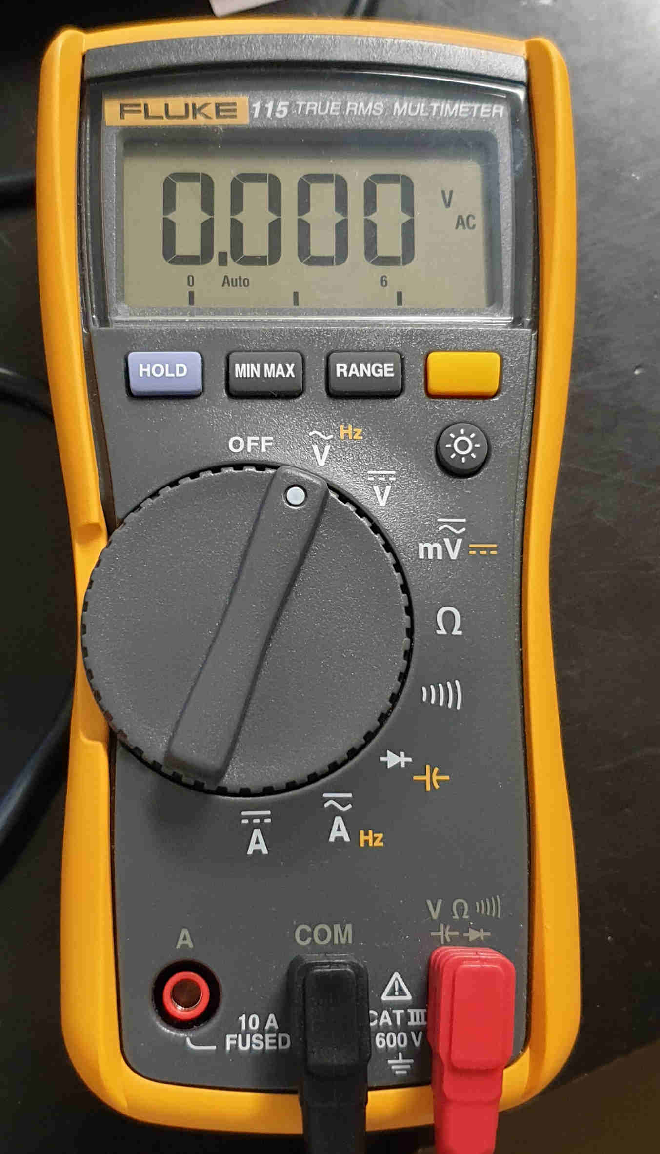
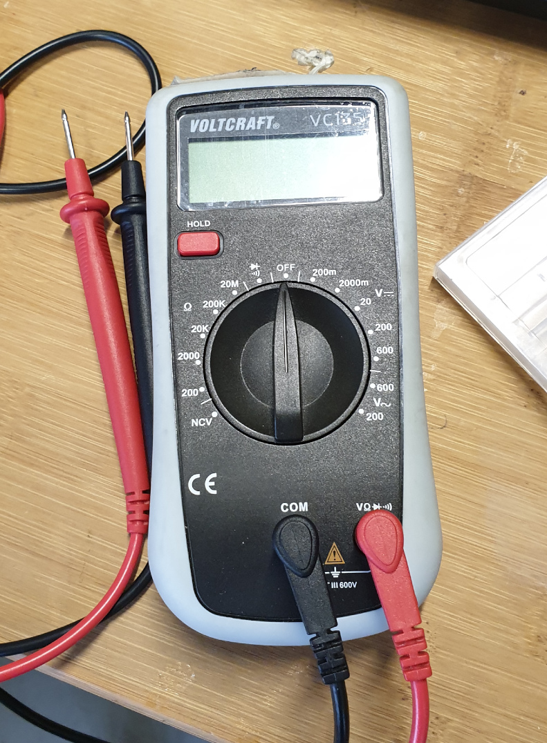
As you can see on first picture this is FLUKE 115 multimeter and I put it on first measuring option and that is measuring Volts in AC (Alternating Current), that is an electric current which periodically reverses direction. In my case it is 0, maybe I didn't mantioned but I'm testing with my Hello board which I explained in later documentation and is connected to my laptop.
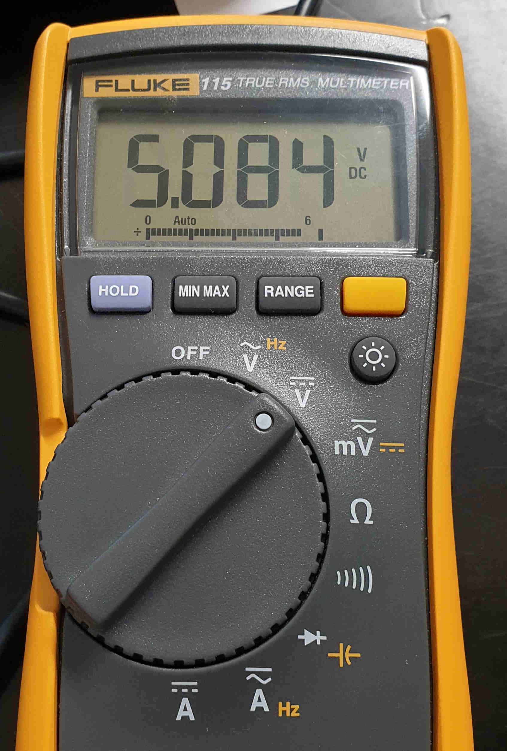
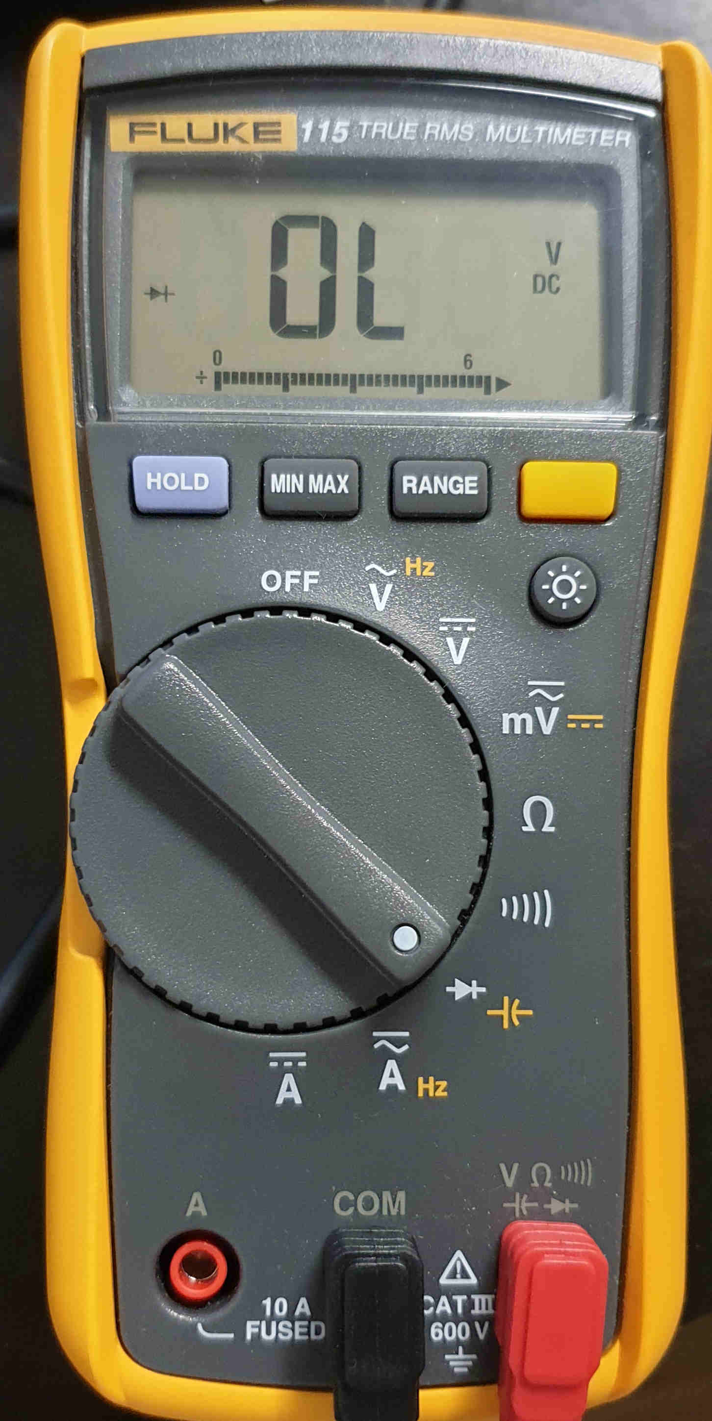
In this case there is some respond and thats because I putted it to measure Volts in DC (Direct Current), bit easier to understand than alternating current. Rather than oscillating back and forth, DC provides a constant voltage or current. So on picture you can see that through my board is flowing 5V.
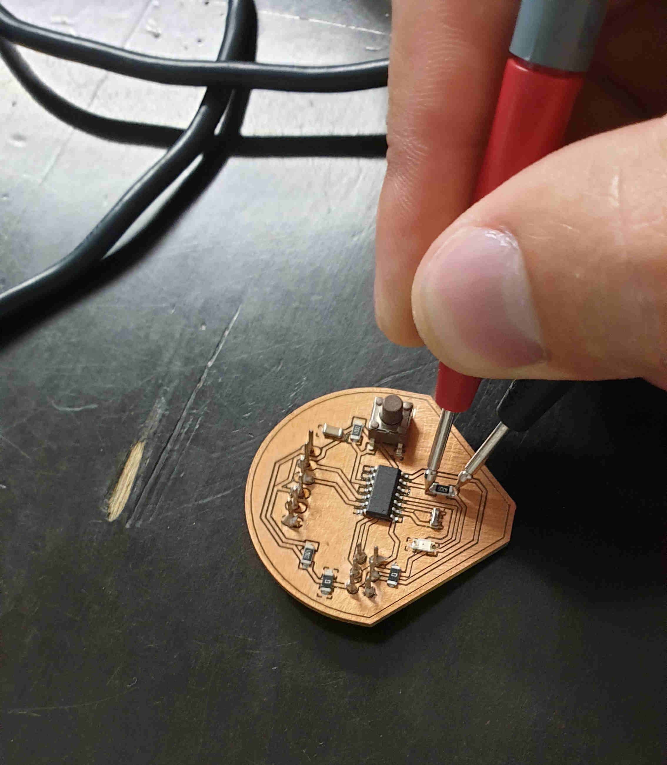
This is also explanation how am I eassuring all of that and taking pictures, I'm holding them like chinese chopsticks with one hand and with another taking picture. For this I wanted to see how it looks when you want to measure resistance, so I need to put it on Ohm sign and put one measuring stick on one side and another to other side of resistor, as expected resistance is near 470 ohm.
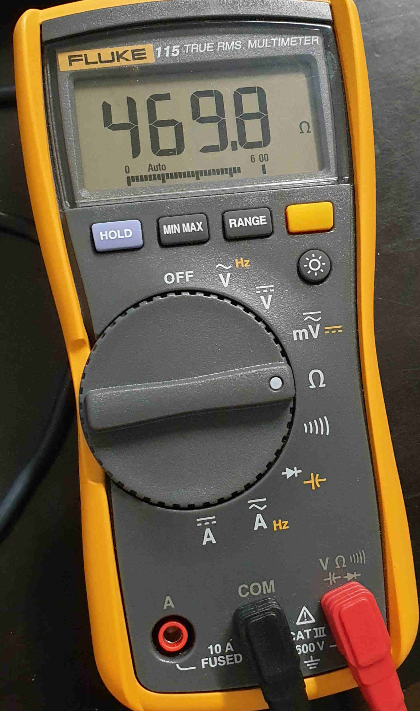
Picture abowe reprisents measuring of diods. A diode is best tested by measuring the voltage drop across the diode when it is forward-biased. A forward-biased diode acts as a closed switch, permitting current to flow. A multimeter’s Diode Test mode produces a small voltage between test leads. The multimeter then displays the voltage drop when the test leads are connected across a diode when forward-biased.
And for the end one of most usable option on multimeter that we use in lab is sin like sound, between resistance and diode measuring. This mode is used for checking all connections on your soldered PCBs, it helps prevent short cuts when connecting to power supply. I would say this is most important step in producing PCBs and always double even tripple check your connections, it can save you a lot of time and material.
INIVIDUAL ASSIGNMENT
This weeks assignment was to redraw echo hello board, but to ad at least button and LED, also with current limited resistor.
EAGLE
To have the board that works I first need to make one…so let's start with opening EAGLE and redrawing the board. All important commands for EAGLE you can find in my „Electronics production” week5. There I was explaining how to ad library and so on. But I'll also explain it here shortly.
After openning Eagle it is time to pick all components that I’m going to need for making this to work so the picture of all needed components is below.
To access the library the direction is: “Edit-Add…” or faster way is to press on the left tool bar icon with green plus and sign for pluger. To add the file in EAGLE I have to: “Edit-Add-Open library manager-Browser” and pick downloaded file.
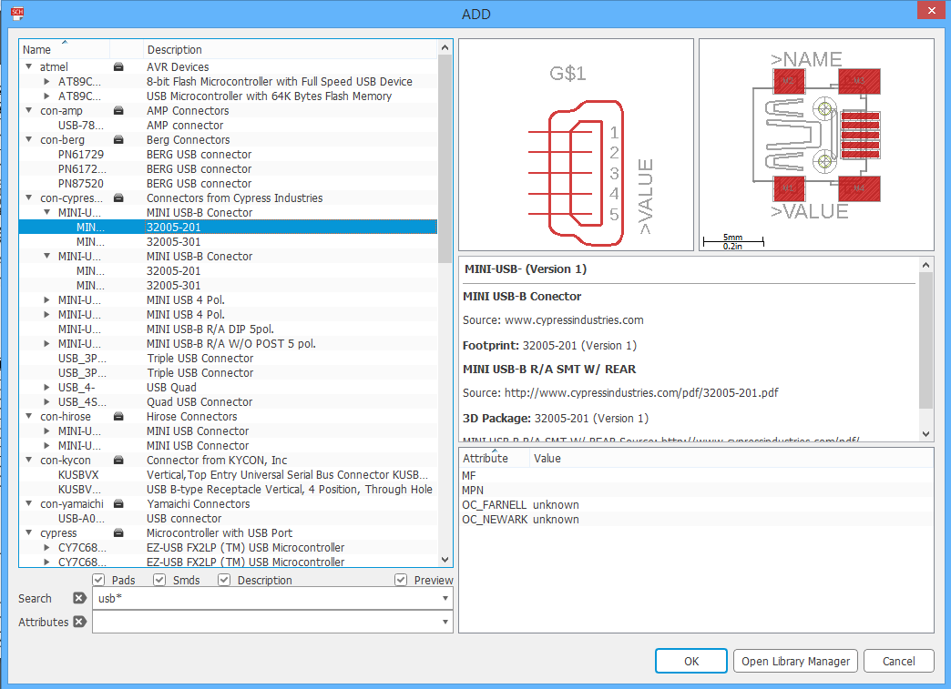
This is the library of all available components that you got with the EAGLE, but there is not always all components that you need so you have to search trough the internet to find that missing part/s and to download it.
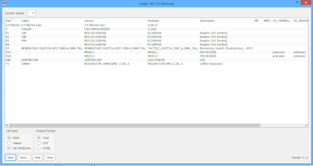
The preview of the BOM(Bill of Material) is available after you pick up the component, that my colleague and I had to discover by ourselves over the internet and by looking into the live components. To access the BOM window I have to go to: FILE-RUN ULP and in the search bar type “bom”, press open and the window with BOM will appear.
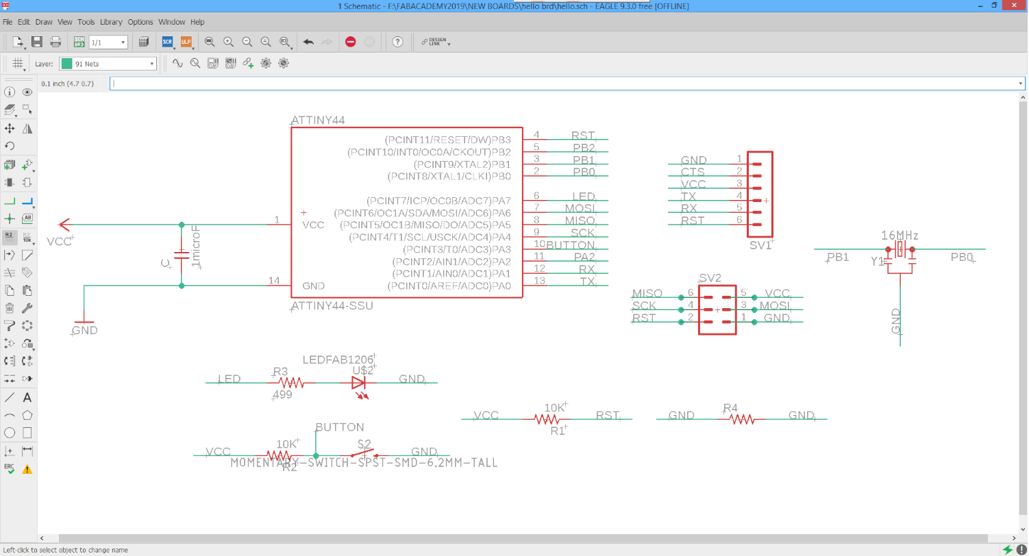
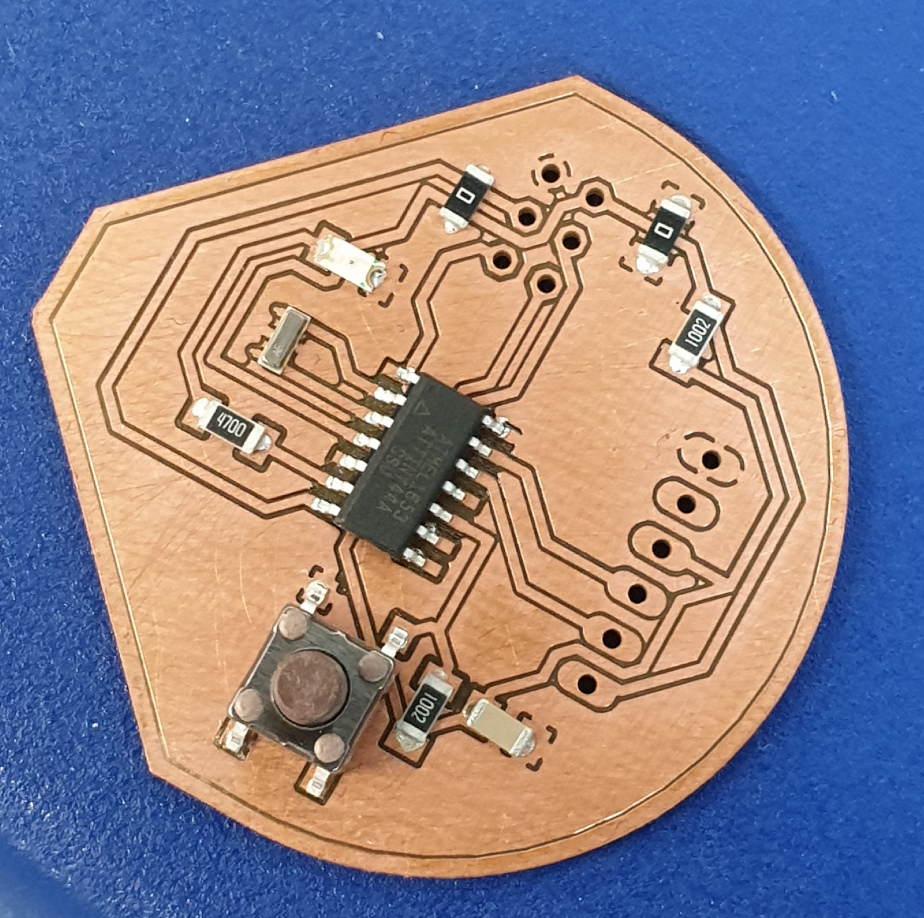
This is the final look of schematics with added LED and button, as you can see there is one resistor that has both sides connected to the ground, that is 0 ohm resistor that I added after struggling to reorder my components in board view that looks in the end like this.
After the check I can go to Board layout: “Window-Board”(green icon “BRD”). Now comes the hardest part for me in making my board. At first I was just looking in the monitor and was confused, a lot. But with a lot of help from my instructor Tobias, I figured out how it works and what I should do and what not. Eagle is using automatic rerouting so it's a lot easier to connect components. Widh of routs and gaps betwean them can also be changet, depends what you want and need.
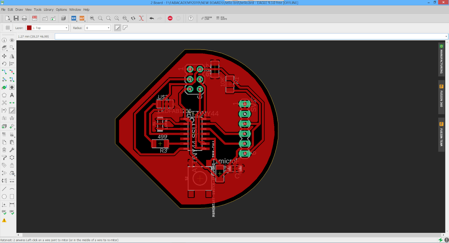
So below you can see my final look of my board in Eagle board view.
BOARD PRODUCTION
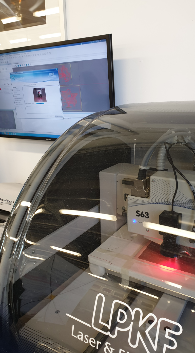
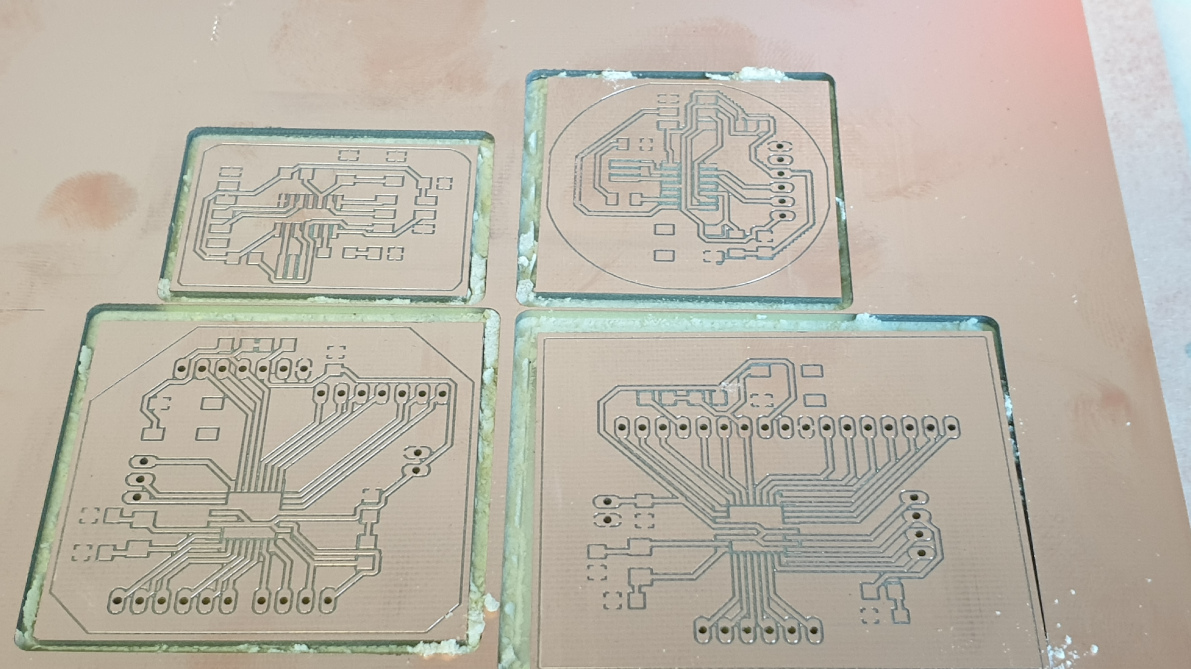
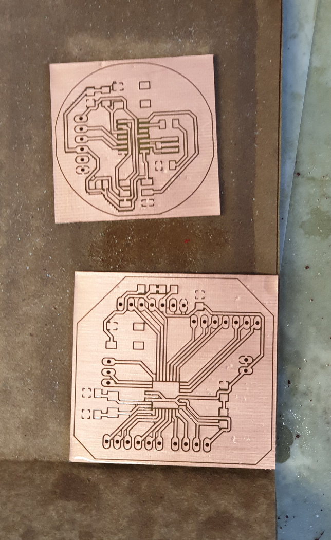
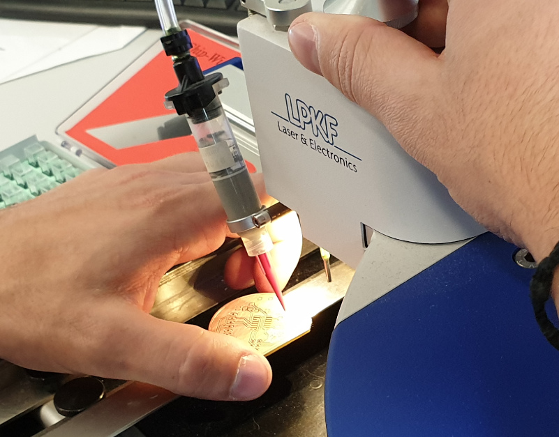
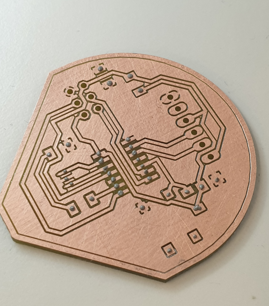
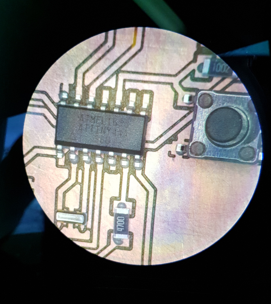
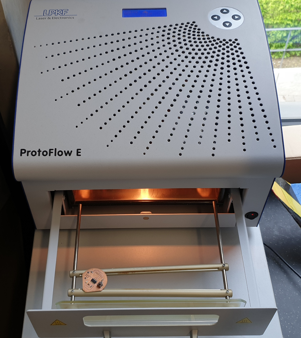
Board production part can also be seen in my week 5 assignment. How is it going step by step and all about Pick and place LPKF machine, mill and how to use them. After milling the board I sprayed it and left to dry for several minutes. Than the board is prepared for solder paste…where I noticed that I’m missing something…my LED and resonator wasn’t connected to the ground, so I added second 0 ohm resistor which I’ll also show on the picture. Reminder for the next time is to triple check everything😊. Putting the components with tweezers and microscope was easy and a lot of fun. Like in week 5 after the all components were on there place I need to put the board in the reflow oven so the solder paste hardens. At the end I only have to solder pins to my board and it’s ready for programing.
When the board was soldered and ready, there is one more step to make before I can program it. Need to test al the connections and make sure that all the connections are soldered good and that there are no connections between wrong traces. I’ll test it with multimeter. As I could assume there was two pins that weren’t connected right so I solder them again and after that the board is ready for programming.
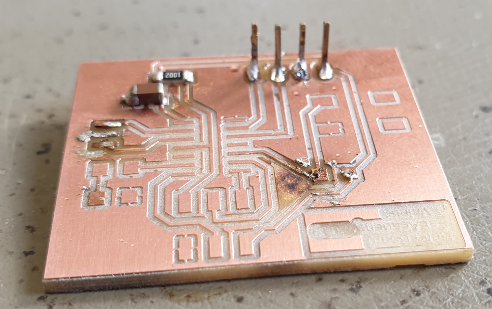
But this week was very interesting and a little bit stressful for me because my first attempt was at FabLab Kamp Lintfort and there they don’t have a pick and place machine and they are not using soldering paste for the components. They are soldering all by there own and in the end I’m appreciating that more because we have to practice our soldering skills and in the end it’s not that hard, you just need to have patients. So the picture below is representing my first attempt to solder SMD components, as you can see I burned it hard time, unfortunately didn't take a picture after that when I remove some of traces by accident.
PROGRAMMING
After learning the lesion and burning first board, It’s time to program Echo hello board. So first things first I need to download “.make” files, I’ll put them below. If that's not woking here is LINK and just under "host communication". To download them just “save link as” and save it where you want, for me it was my folder for this weeks assignment just so I don’t forget where did I put it.
hello.ftdi.44.echo.c hello.ftdi.44.echo.c.make
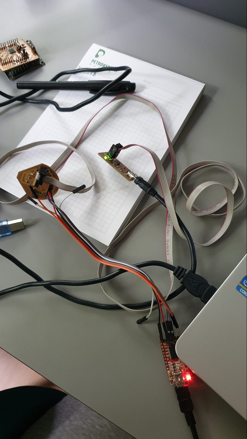
Now I need to connect my FabISP with Hello Board and also FabISP to computer and Hello Board to computer but using the FTDI connection. Just like on the picture below.
When that’s done, next step is to open GIT Bash in that folder and ran this three commands, so the “.hex” file is made like in Week 5 and it’s also made “.out” file.
“make -f hello.ftdi.44.echo.c.make”
“make -f hello.ftdi.44.echo.c.make program-usbtiny-fuses”
“make -f hello.ftdi.44.echo.c.make program-usbtiny”
Next steps are:
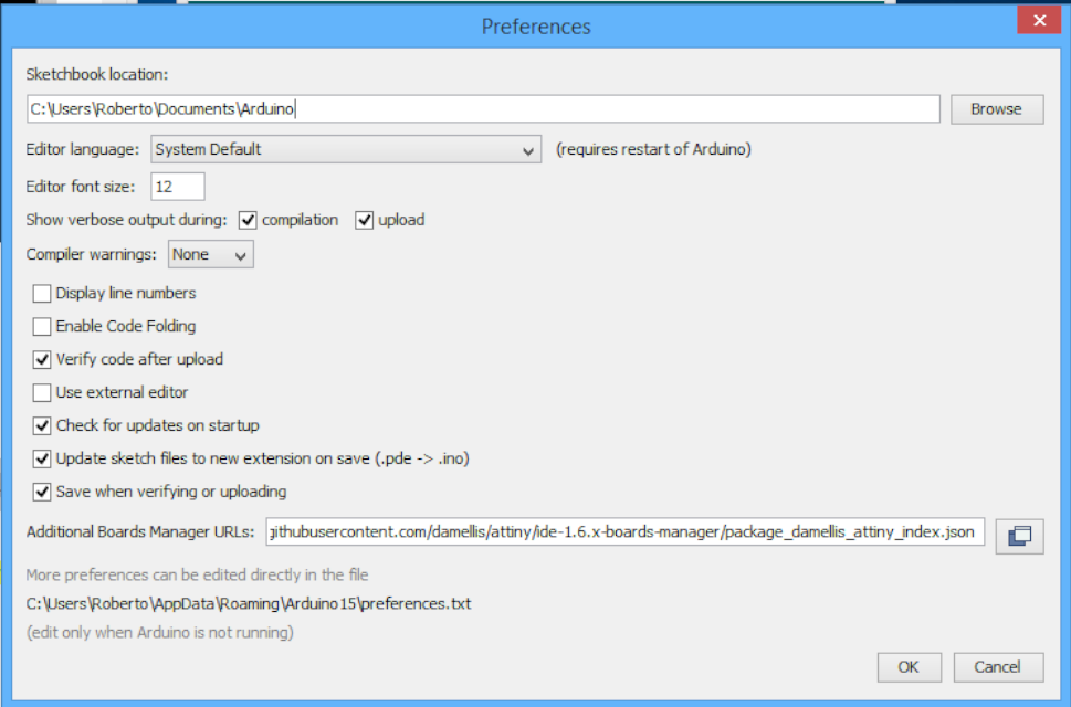
1. Open Arduino IDE
go to “file>preferences”, at “Additional boards manager URLs” paste this link (https://raw.githubusercontent.com/damellis/attiny/ide-1.6.x-boards-manager/package_damellis_attiny_index.json)
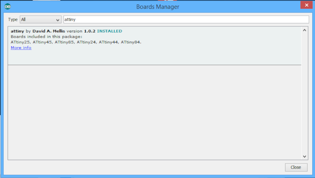
2. Installation of ATiny package
“tools>board>boards manager” than I need to search for “attiny by David A. Millis” and to install it. After doing that, again in “tools” I have to pick the board that I want to program, type of clock and also is important to use correct port(had a short struggle with that at the beginning). Also it’s important to select programmer that I’ll be using, so that’s my USBtinyISP(FabISP) that I’ve made on Week 5.
3. BURN BOOTLOADER
Now are things getting more interesting. “tools>burn bootloader”, at first attempt I got error massage on the bottom of the window, it says that board at chosen port is not available, so I checked again the ports and change it to correct one, then I got confirmation massage.
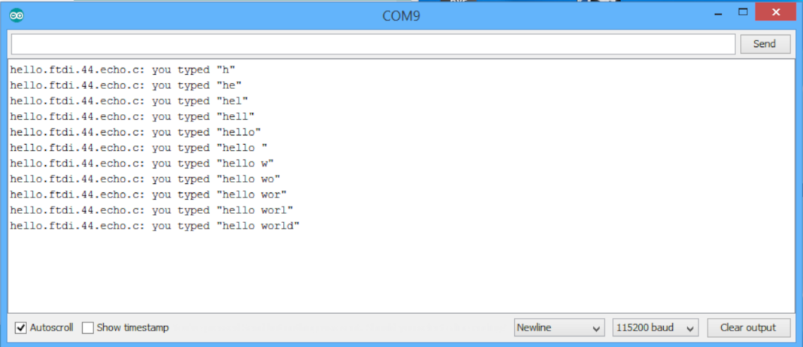
4. FINAL STEP
“tools>serial monitor”, with that new window has opened and is time to write letter by letter and see what’s happening.
After successful attempt I wanted to try one simple simulation of blinking LED, just to finish this assignment with bigger smile. “file>examples>basic>blink” and upload.
*EASY EDA*
After finnishing my assignemt for this week, I wanted to try one more CAD software for making PCBs. Than searched on internet and got to this very interesting one and it's onlyne so it diesn't have to be download. It's Easy EDA. Online open soarc CAD.
And it's simple to use it, it also got tutorial with basics right away when you open it. Just like the example below.
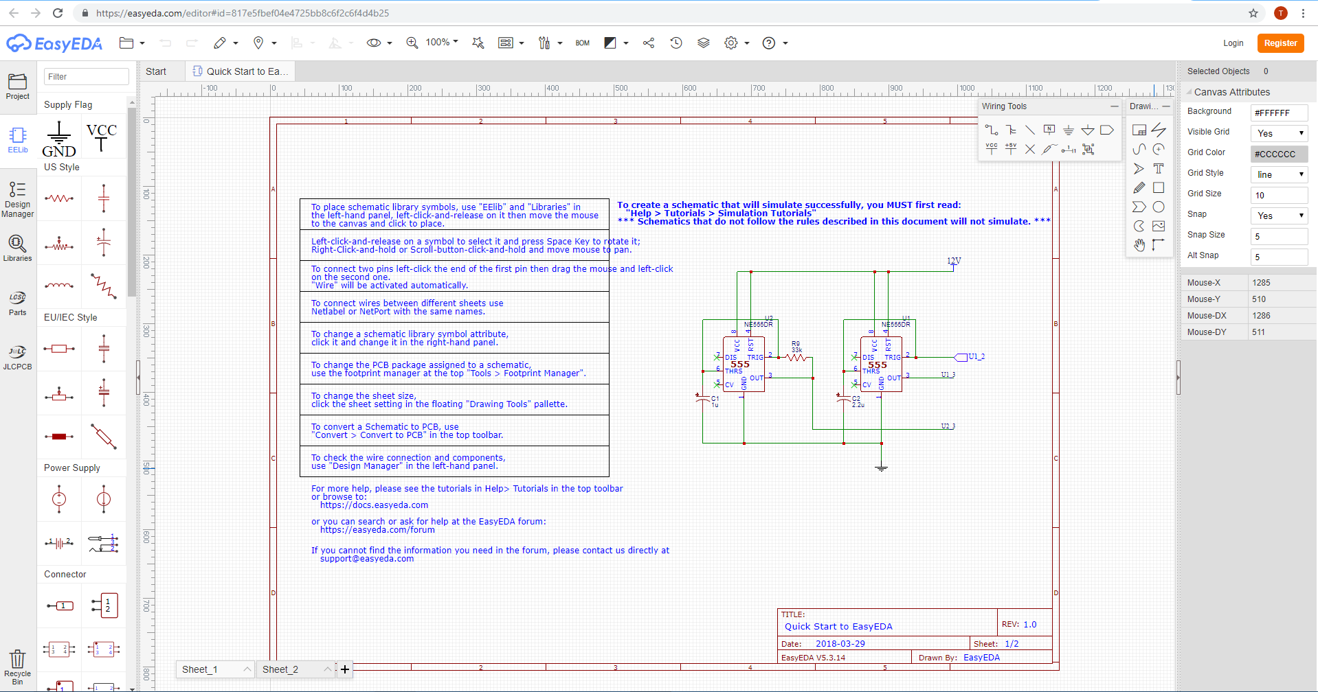
To put the component you want, just need to pres and drop when you want and it's easy to find components toolbar, it's on left side of the window. Traces for connecting components are on right side but you can move them to the place where they are not getting in your way. After finishing schematic, BOM(bill of materials) can be found on top of the winow, there is icon that says "BOM". To transfor it to board design, have to go also on top of the toolbar where is icon to transform to board design or even to upload finnished board design.
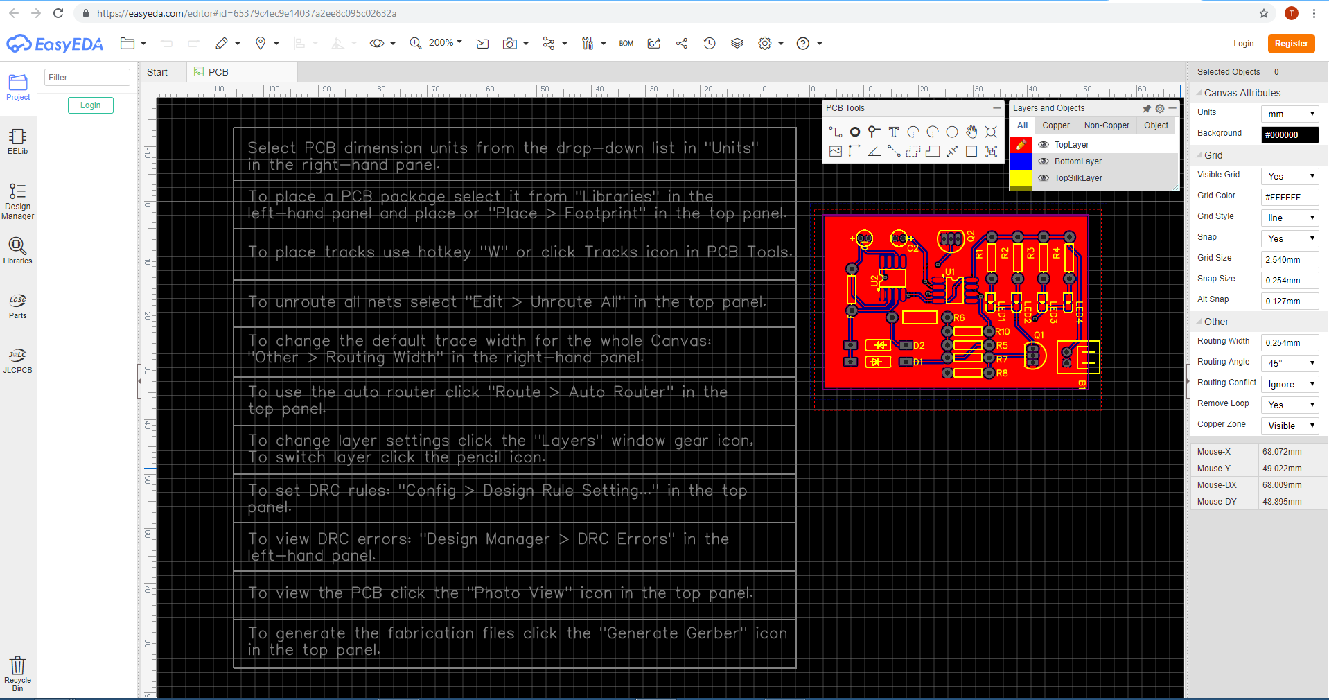
In board design you can like in EAGLE connect components, remove them, change their names and values, set the settings to auto rout, so it's lot easier for you and quicker to conect everything. The layers can also be changed to get better priview of your board.
Think this is a great online CAD software, also easy to use, good eplanations in tutorial righ away.