ELECTRONICS PRODUCTION
5.WEEK
GROUP ASSIGNMENT
PREPARATION
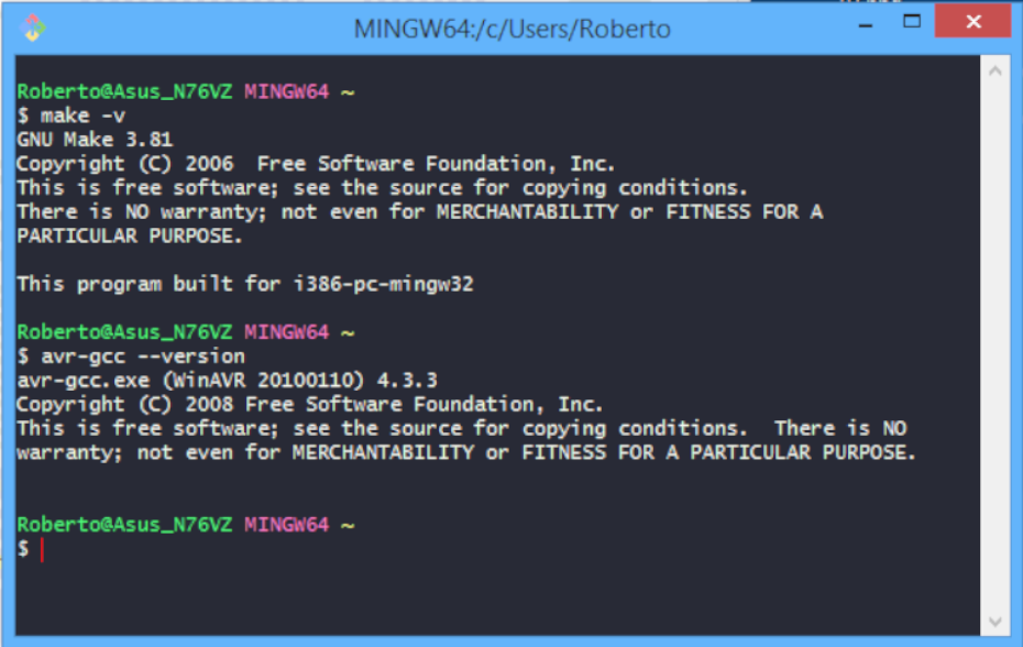
First of all my knowledge of the PCB production was below zero before the lecture, so I was going in this assignment with full focus and dedication. But of course there was a lot of confusion at the beginning :). Our task for this week was to build our own FabISP programmer and try to make it workable. In this assignment we are going to use different tools, so lets start from the first step in making in-circuit programmer…
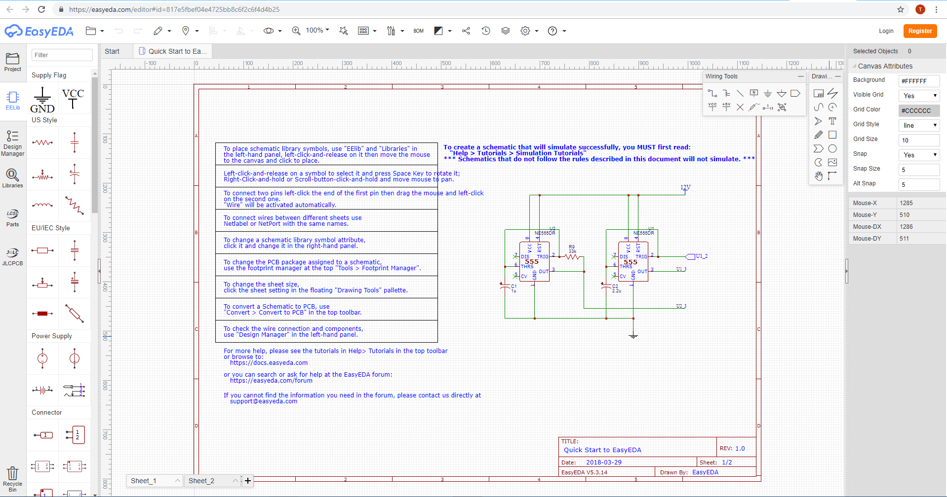
1.EAGLE
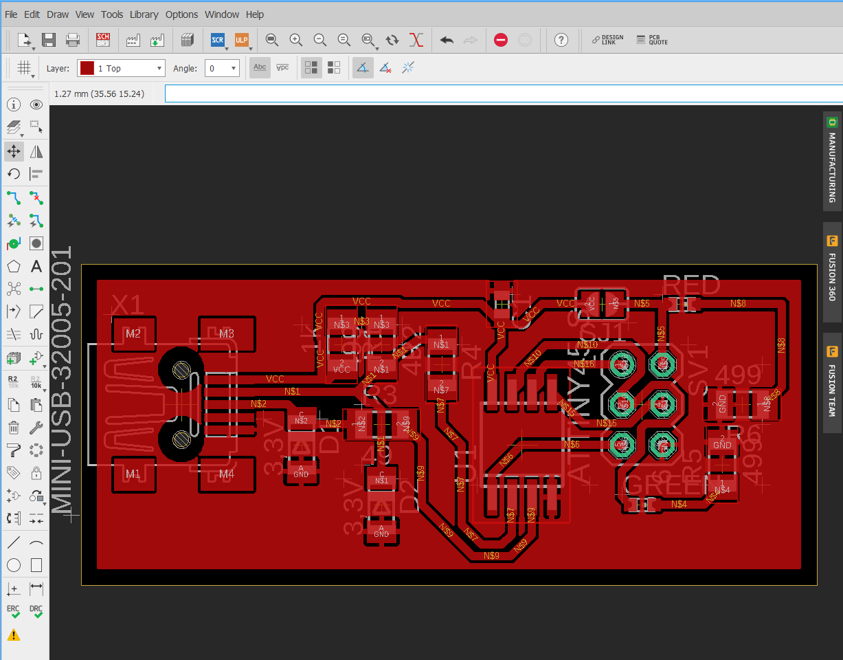
For designing my PCB board I have to install EAGLE, design software by Cadsoft Computers and it’s suitable with Windows, Mac and Linux. EAGLE is acronym for Easily Applicable Graphical Layout Editor.
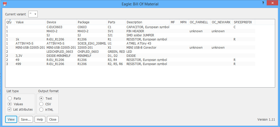
After the installation it is time to pick all components that I’m going to need for making this to work so the picture of all needed components is below. The preview of the BOM(Bill of Material) is available after you pick up the component, that my colleague and I had to discover by ourselves over the internet and by looking into the live components. To access the BOM window I have to go to: FILE-RUN ULP and in the search bar type “bom”, press open and the window with BOM will appear.
To access the library the direction is: “Edit-Add…” or faster way is to press on the left tool bar icon with green plus and sign for pluger.
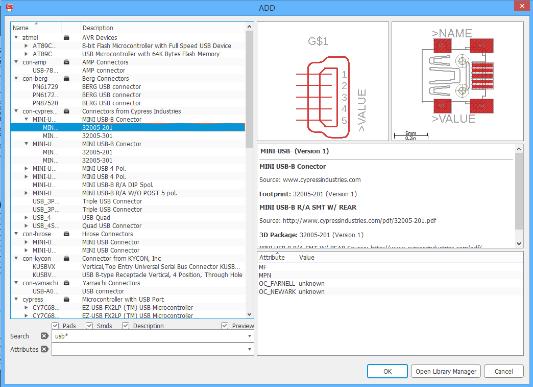
This is the library of all available components that you got with the EAGLE, but there is not always all components that you need so you have to search trough the internet to find that missing part/s and to download it. Colleague Patrick and I didn’t find the ATTiny 45 in library so we searched and find it on DIYmodules. To add the file in EAGLE I have to: “Edit-Add-Open library manager-Browser” and pick downloaded file.
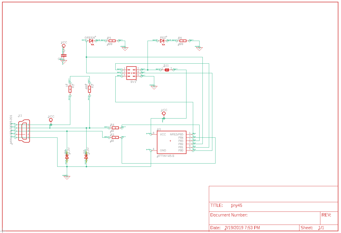
This it how it looks when I added all required parts on connection scheme and connect them on base of theBrians model.
After the check I can go to Board layout: “Window-2Board”(green icon “BRD”). Now comes the hardest part for me in making my board. At first I was just looking in the monitor and was confused, a lot. But with a lot of help from my instructor Tobias, I figured out how it works and what I should do and what not.
So this is how it looked before instructors pointers…
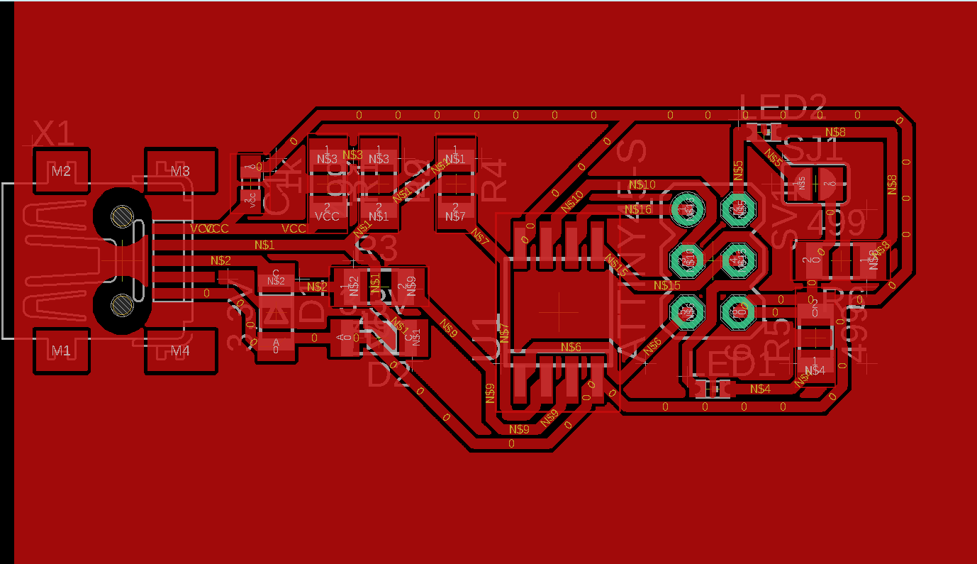
And this is how it looks now…
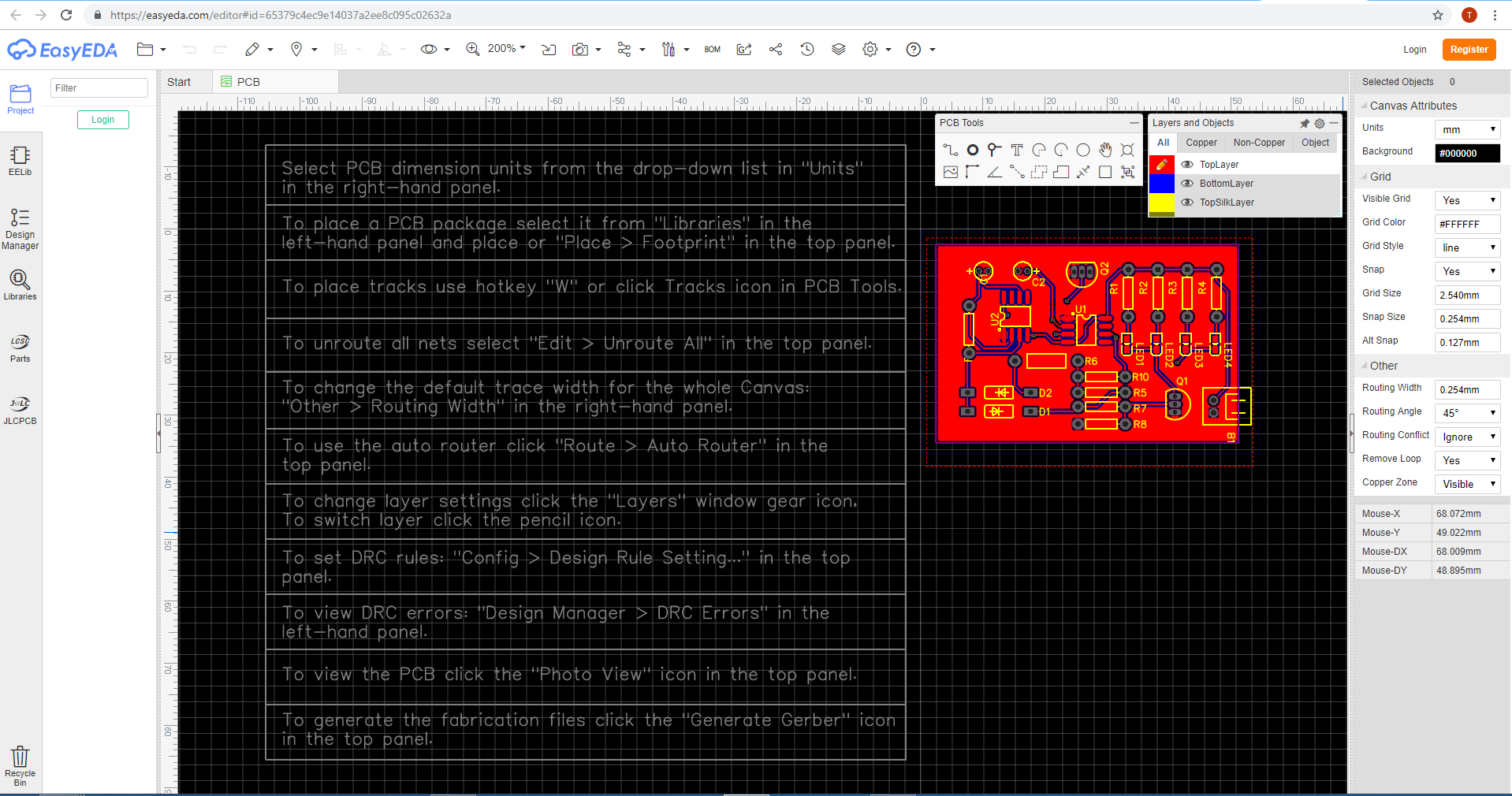
2.MILLING PCB ON LPKF
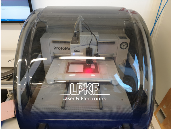
To mill the bord I used LPKF ProtoMat S63, that is suitable for almost all applications of in-house prototyping. This type of mill in our HRW lab works straight from CAD data to process boards. Features include camera which aids the user with front-to-back alignment for double-sided and multilayer PCBs, and an automatic tool changer for expedited board production. LPKF ProtoMat S63 uses CircuitPro software that is shown below.
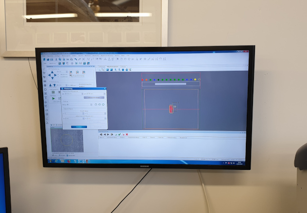
Usage of its software is simple…File/Tamplates-Single sided Top-Process Planing Assistant-Edit Circuit Board(set to: One-sided Top; Material-FR4/FR5; then click Ready). After this I have to choose data from Free Format and select all files with Upper Case endings, now my board is loaded and have to select “Cutting Generator” and select “Isolation method” here I need to choose Single; Pads double and type milling depth. Before starting milling there is couple of steps…Choose “Circuit board fabrication assistant, than I need to press “Start” and “Proceed”. After which the new window will open of the positioning the milling machine, where we pick place with the mouse the place where the board is going to be milled. The whole preparation process is finished so now I can save this CAM-job as “.cbf” file. Now the LPKF starts to picking up the tools and starts to mill.
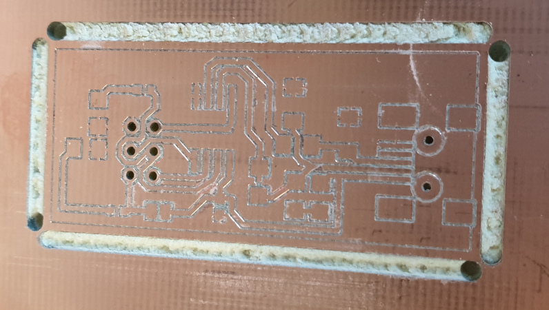
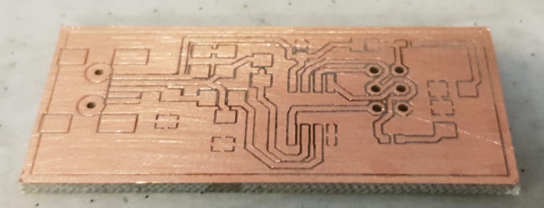
This is the look of my board after the milling. I have to cut the edges with the pliers firs, to detach the board and than I can go to the cleaning process.
3. CLEANING MILLED BOARD
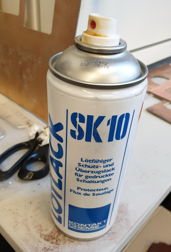
One important step before soldering the components is to clean up the PCB board. We have thisLOTLACK SK10in our lab to fluxes and lacquer-like protective resign for printed circuit boards, but before I sprayed thin layer of that, I polished it.
4. PLACING COMPONENTS ON PCB
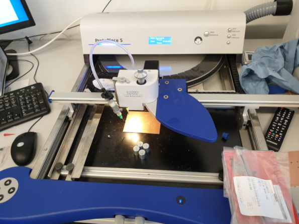
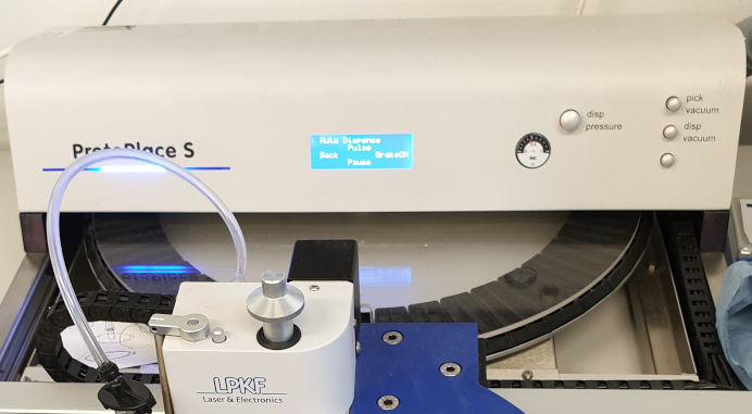
For this group assignment I decided with my colleague that I’m going to examinate theLPKF Protoplace S(well known as “Pick and Place machine”). That is the step in making my FabISP PCB board. For me that was the stresses part of this weeks assignment because you have to be very careful and calm. First of all I had to get to know with the machine and it’s work principles. The LPKF Protoplace S is semi-automatic pick and place system for professional assembling of PCB-s, it allows much quicker assembly than with the tweezers. It is possible to place various components including fine-pitch down to 0,4 mm (16 mil). Precise placing of fine-pitch components is ensured by a x/y/z locking mechanism, micro table fine adjustment and automated placing.
So after I designed my PCB in Eagle and mill it on LPKF mill and cleaning the board and spraying with “LOTLACK SK10”, there comes the process of placing every component on the board. But before placing all components on their place I need to put the solder paste on top of the places where the components should come, just the little drop so the paste doesn’t touch other routs.
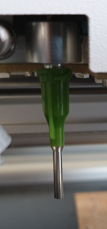
Here is the close-up of the part with the solder paste and the enjection needle. The removable dispenser provides precise dispensing of pastes or glues in manual or automatic modes. Air pressure regulation with time control and the non-drop vacuum function guarantee precise flow, quantity and timing of media dispensing. By pressing the padle on the flore with the foot the machine is compresing the air trough the tube tu the solder paste and extrude it out. The flow of the paste can be regulated on the machine and it depends how big is the board and the parts of the components that should be soldered. Operating air preassure is 0.1 with 4bar.
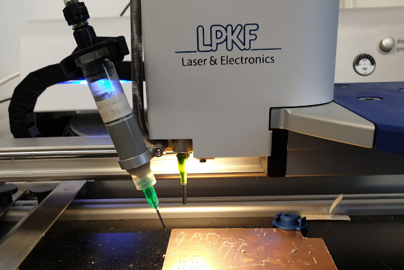
And here is the close-up of the suction needle that is placed right behind the solder paste extruder. Operating vacuum of suction needle is 0-0.8bar.
Another important part of the LPKF P&P is turntable, it’s bad picture but that’s the black round table beneath the LCD screen. It uses for putting the components in the little compartments for better organization and faster work.
When all components are placed on board we have to put the PCB in the reflow oven, which is the next step…
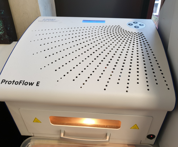
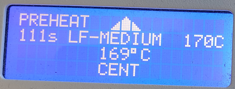
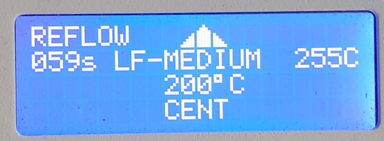
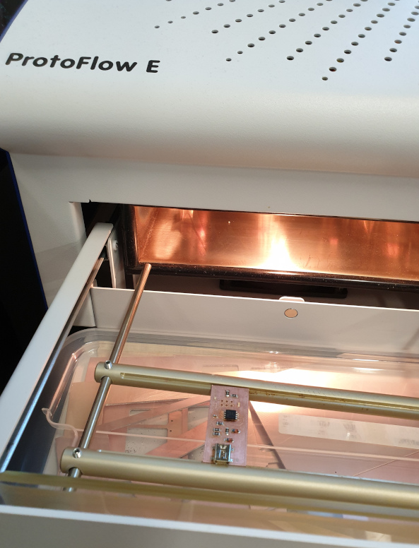
5. CURING THE SOLDER PASTE
For the soldering I used LPKF ProtoFlow E, it’s the ideal oven both for leand-containing and for RoHS-compliant lead-free reflow soldering, curing of the paste in the plated-trough holes, and other thermal processes that need to be controlled precisely. First the oven needs to PREHEAT than the PCB is placed in the oven and the REFLOW starts for 60sec, where the curing of the soldering paste happens, when the time was over I opened the lid so the board and the ProtoFlow E can be cool down.
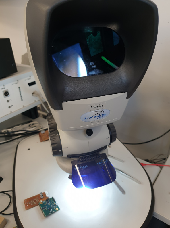
Final step of making the board is to check is everything soldered correctly. For checking the PCB and the soldered parts I used the Lynx Stereo Microscope.
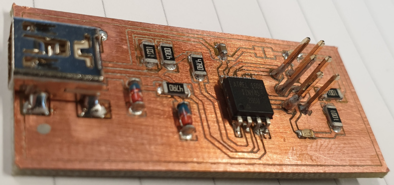
Everything seams good and now the board is ready to be programmed…