Starting to think about my final project - Lamp I went trough several reflexions: 3d printing optimisation of complex geometries - how to modify the geometry of 3d printed object - visualize where to make parts thicker, how to change the shape according to selected 3d printing process /sla, sls, fdm, with supports, without supports,…. something like a smart slicing sw and it can visualize, optimize and propose possible variations of final designs…? for more text *notes scroll down...down...down...
Preview of presentation slide version 1.0
Preview of presentation video version 1.0
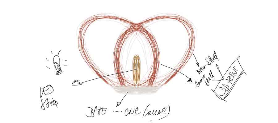
Sketch of preliminary concept idea.
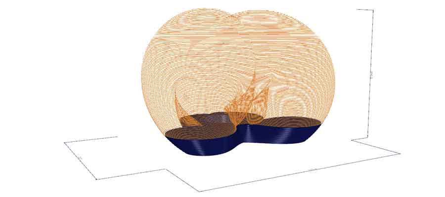
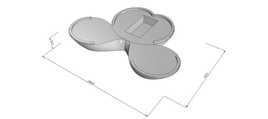
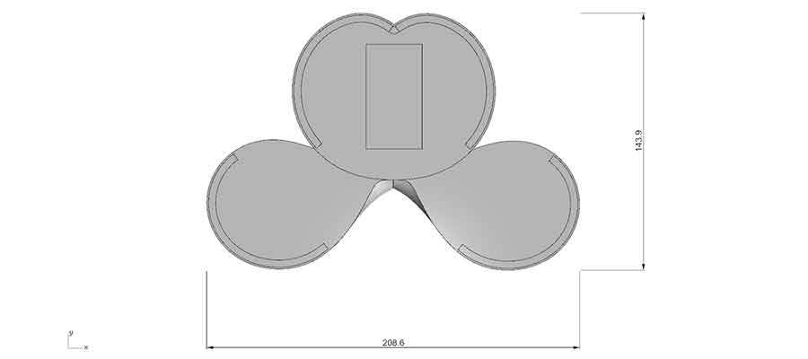
Dimensions.
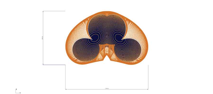
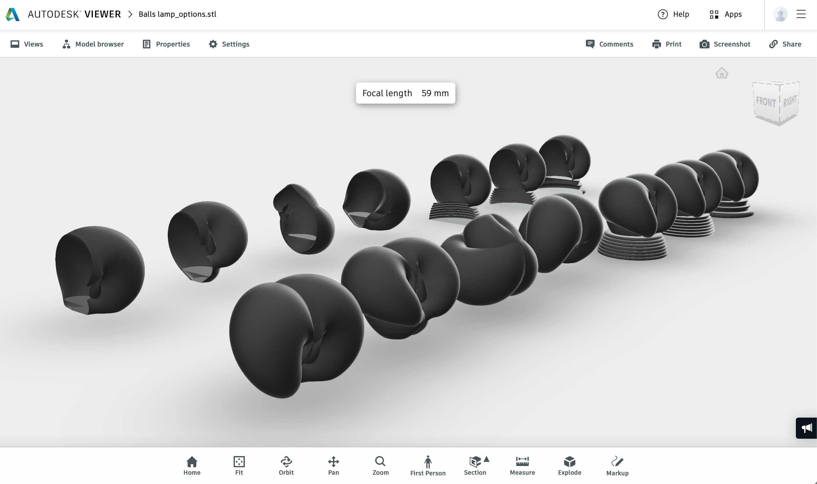
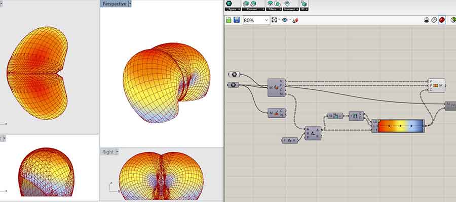
Autodesk viewer offered a free platform to visualize different variations of the shell design for the lamp.
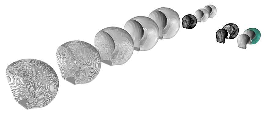
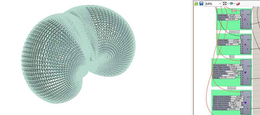
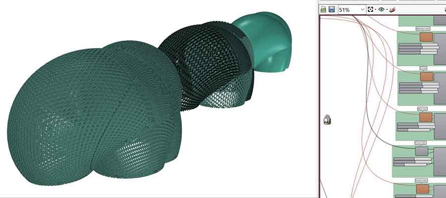
IsoMesh.
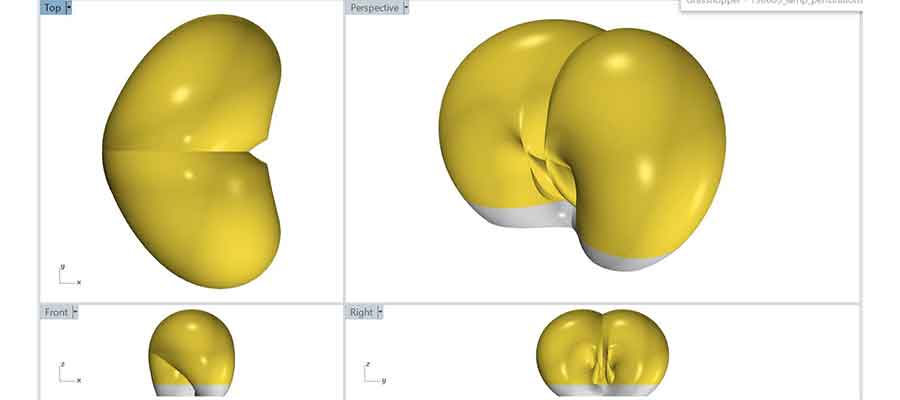
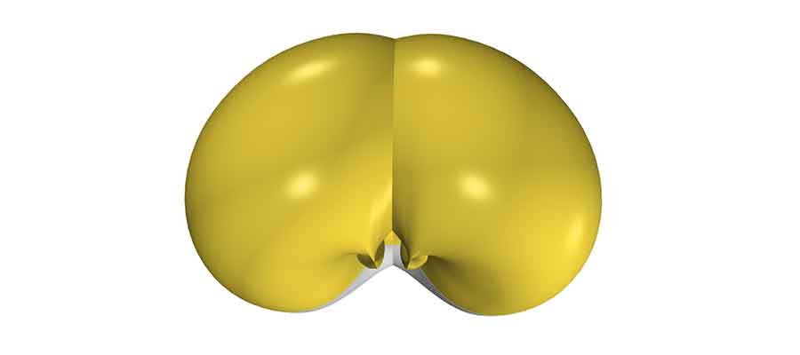
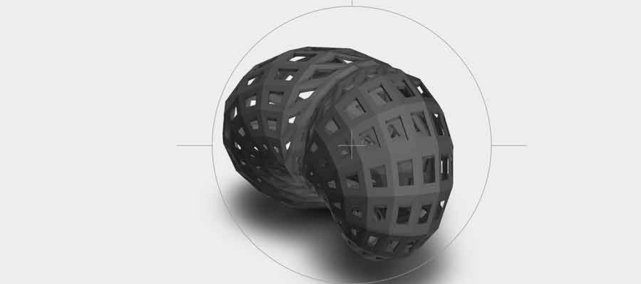
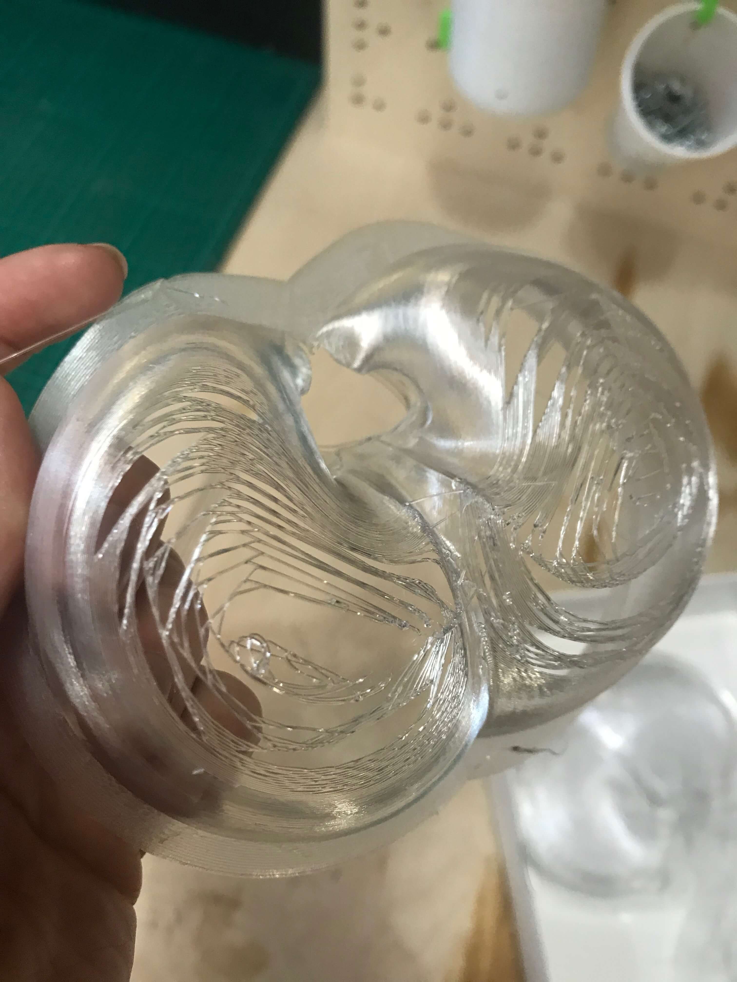
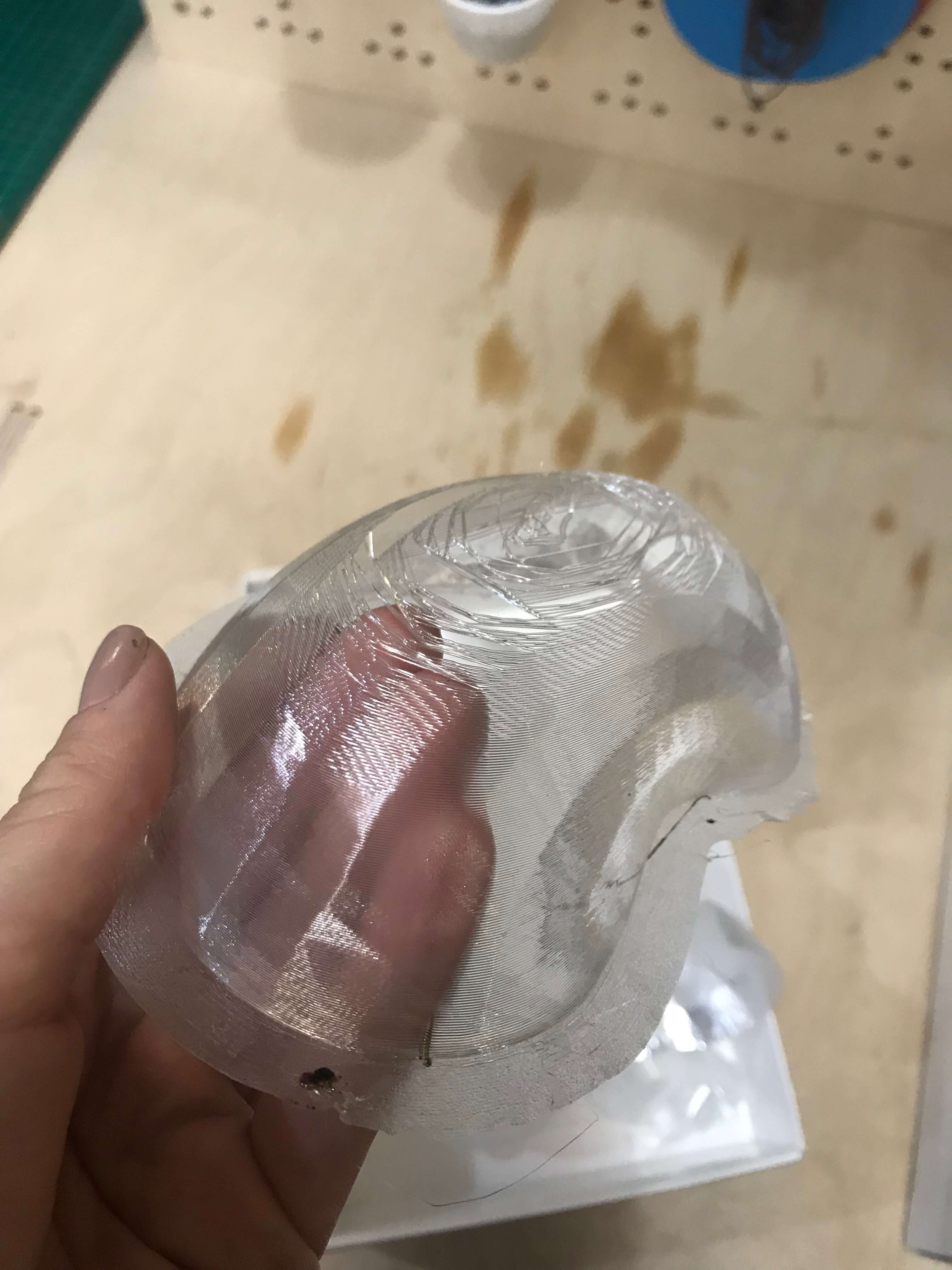
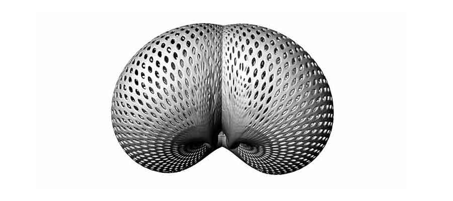
The process of shell designing with perforations.One of possible option with quad perfos.
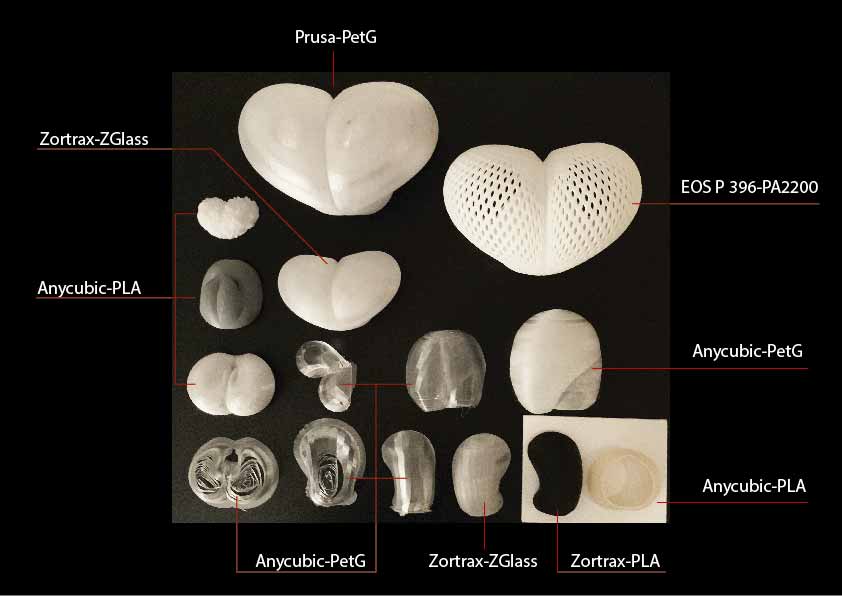
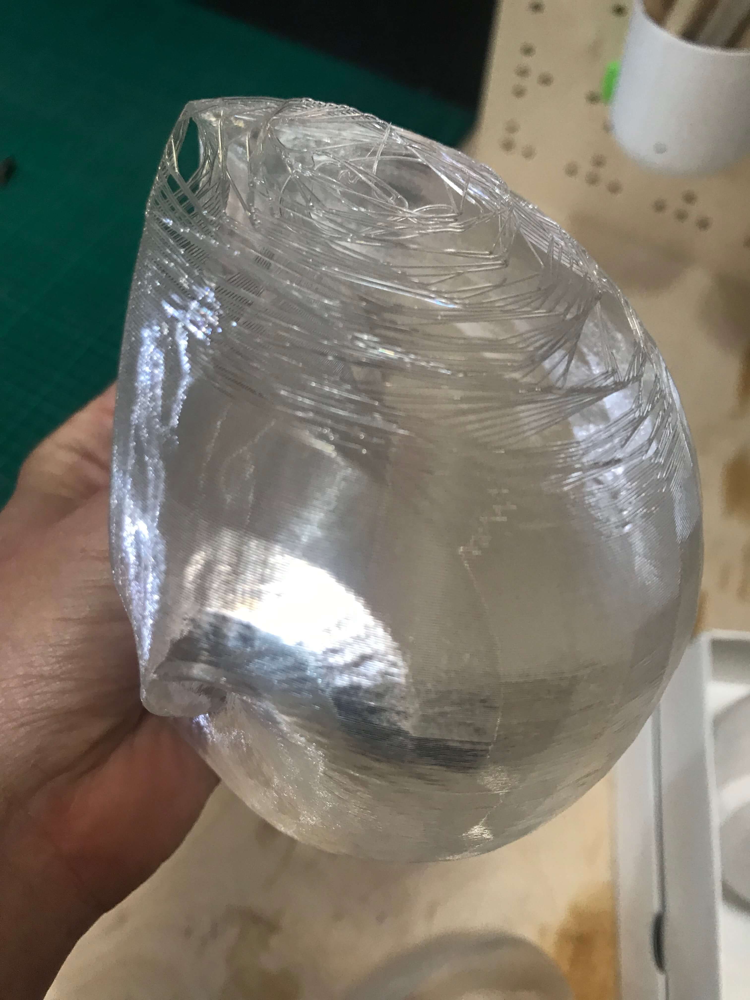
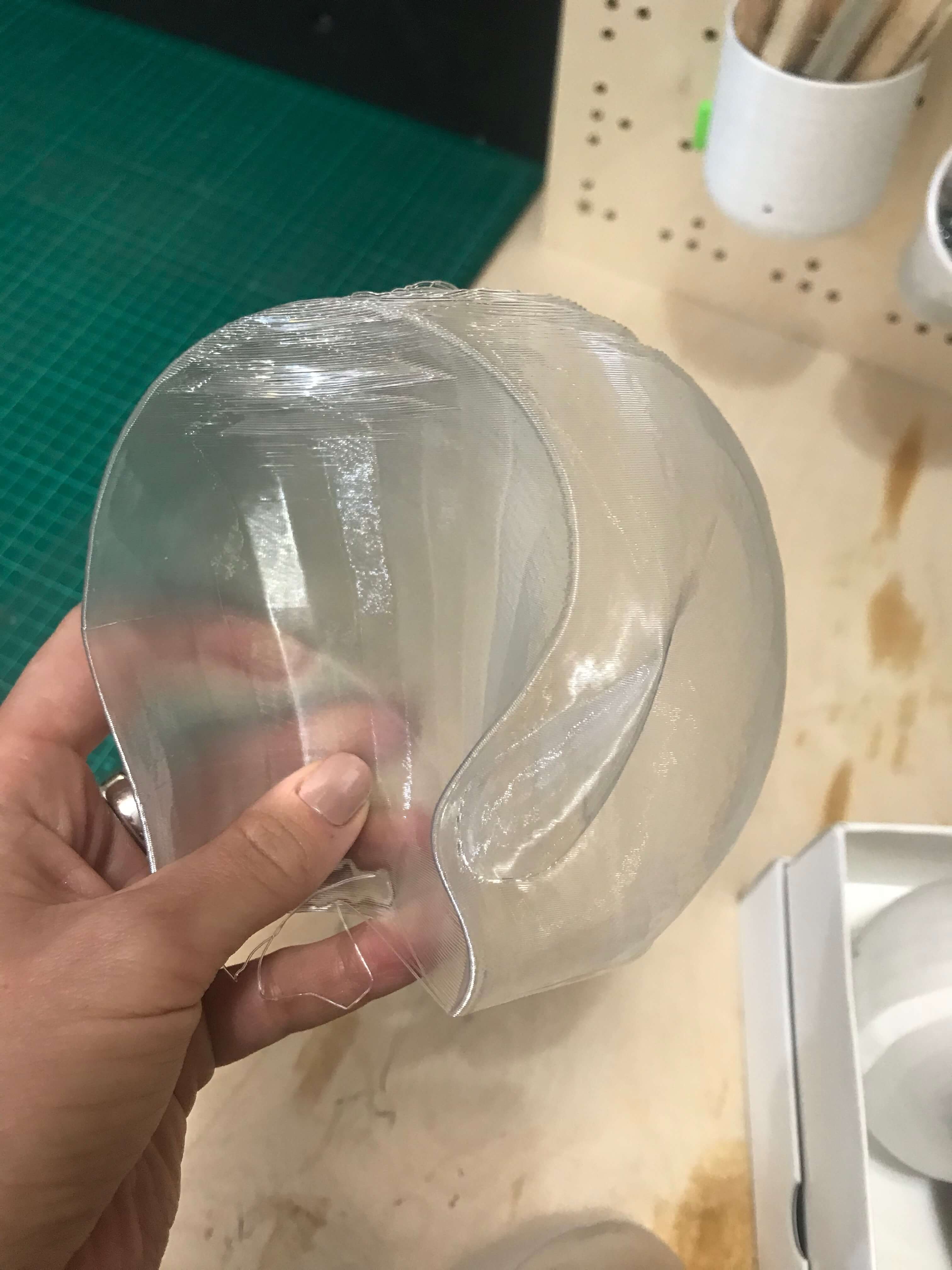
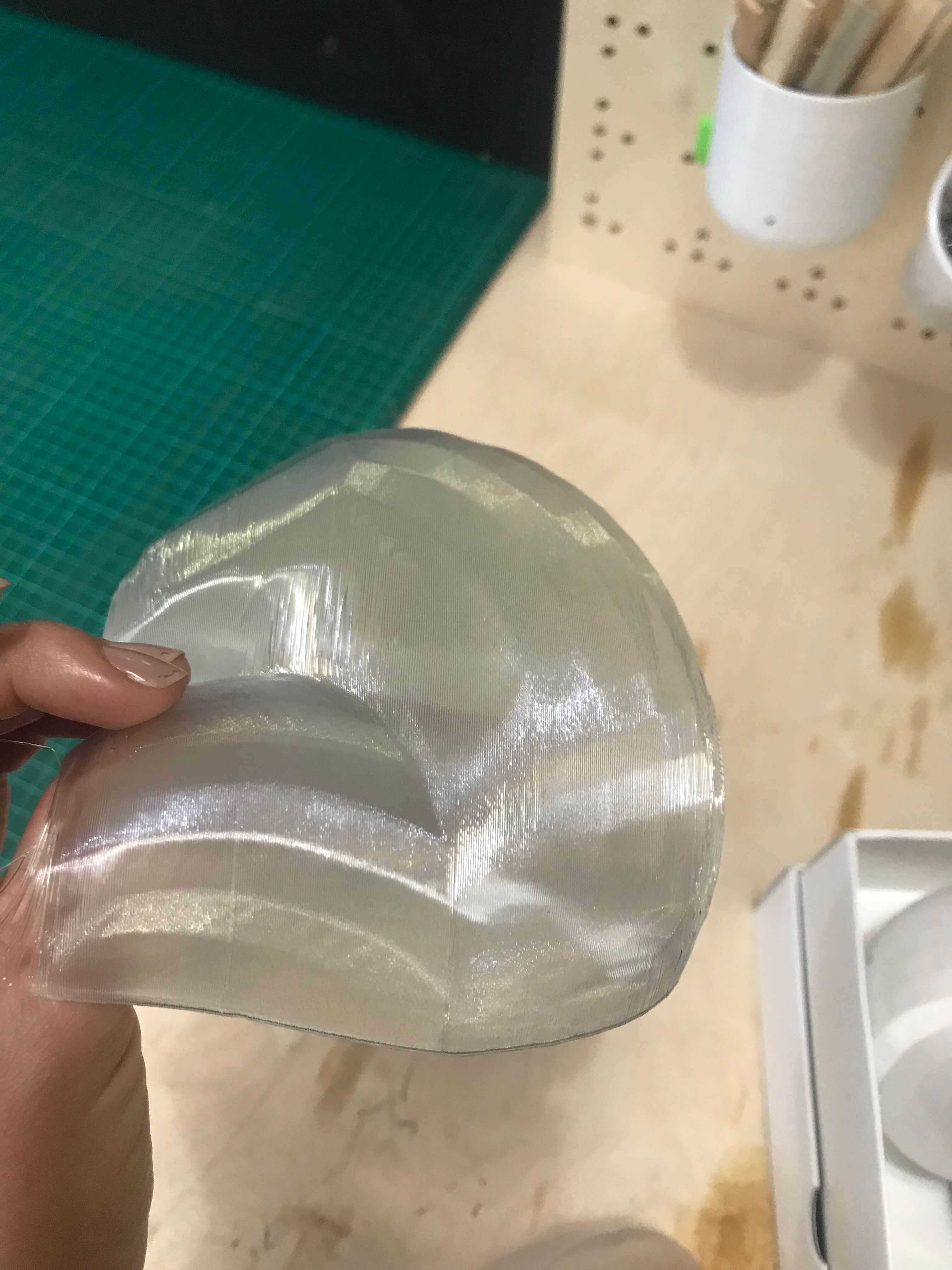
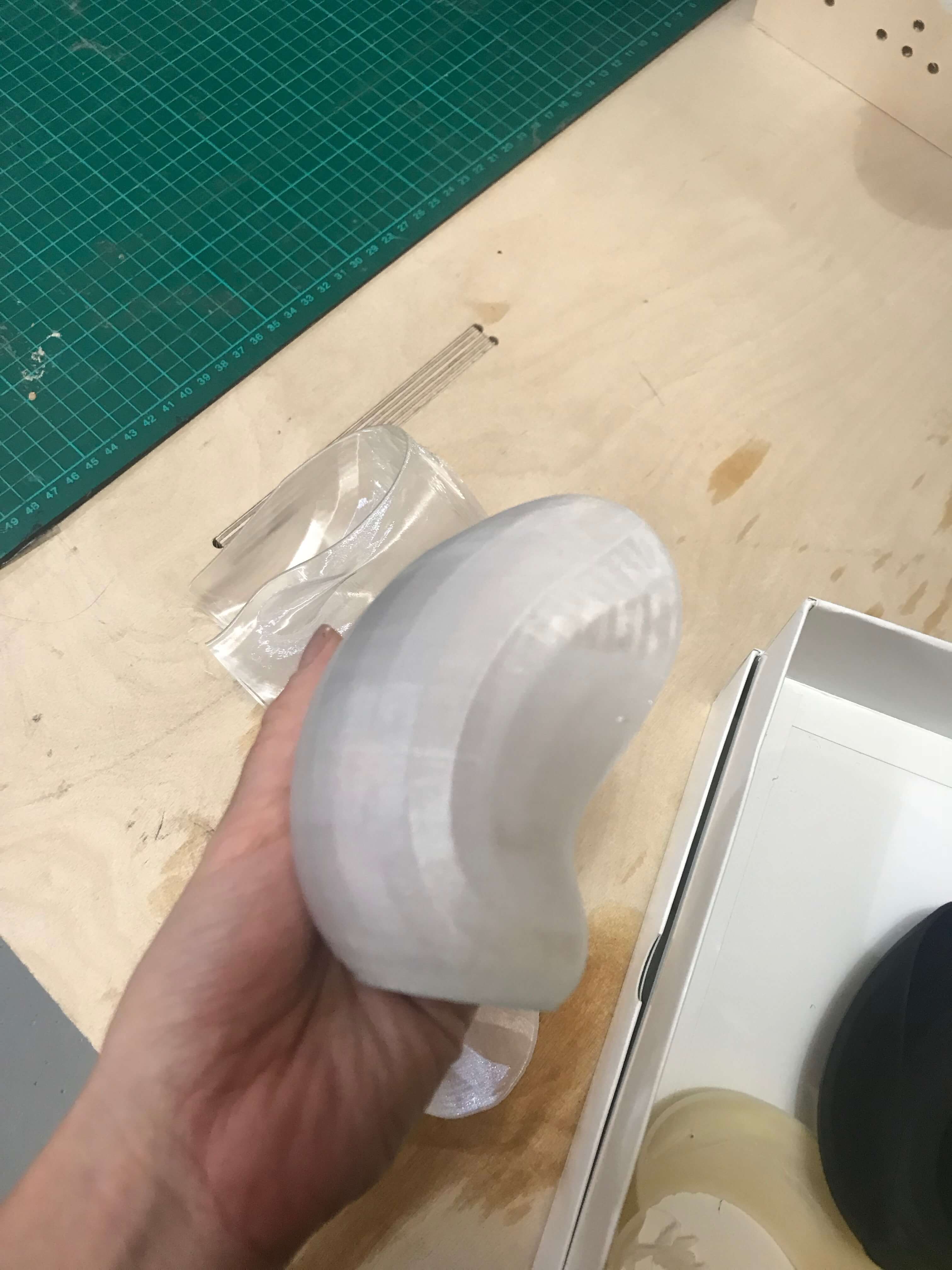
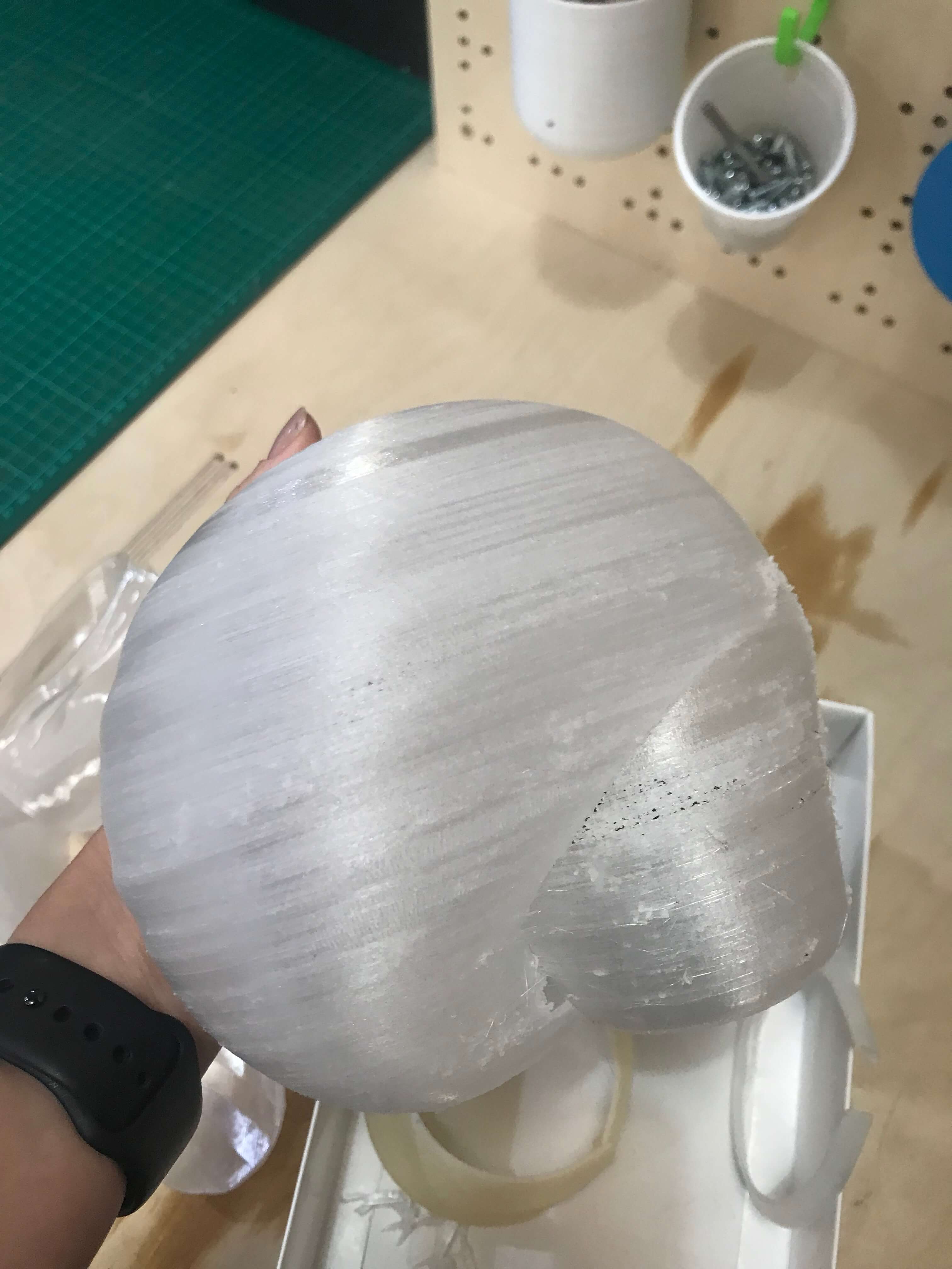
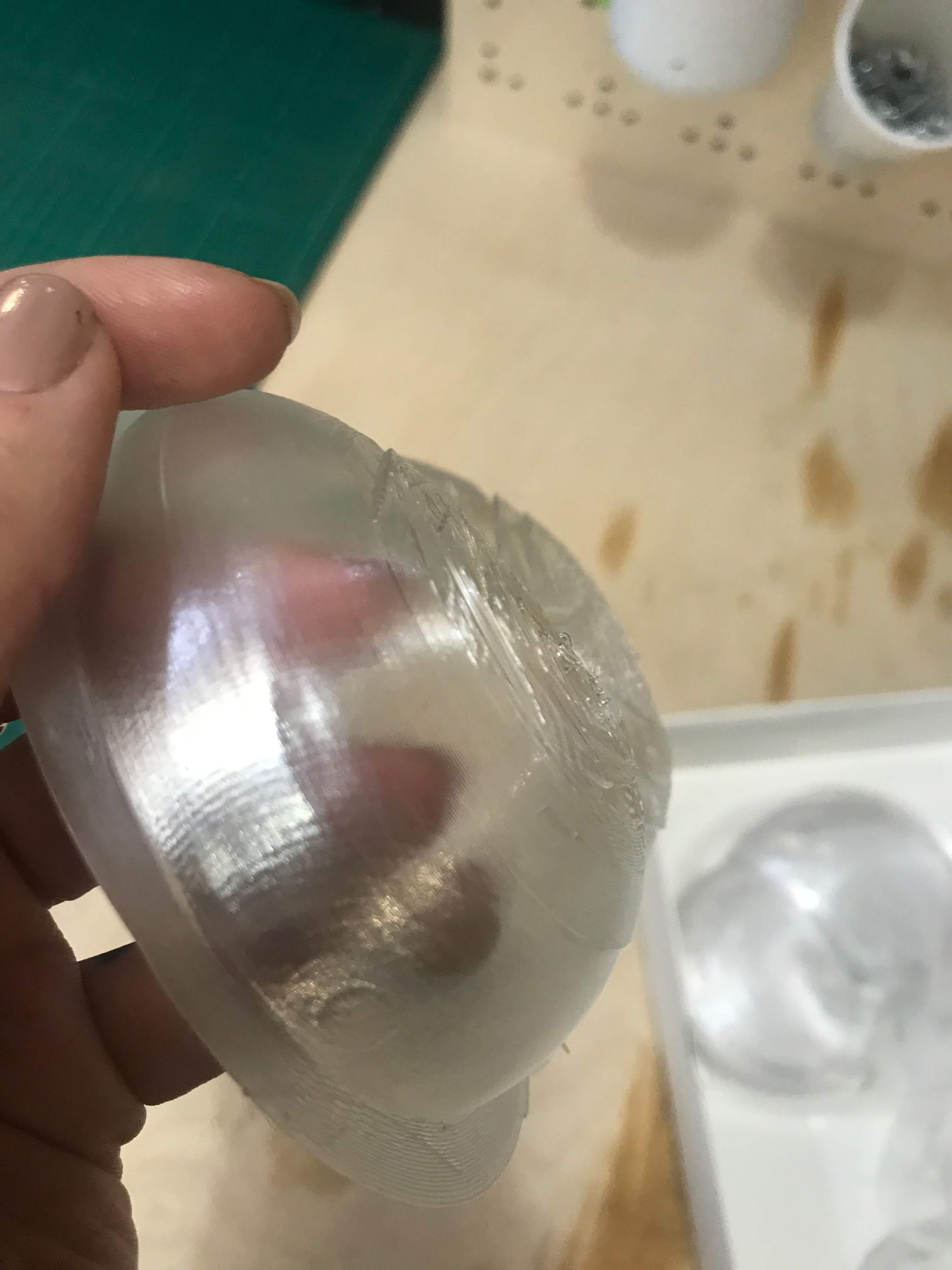
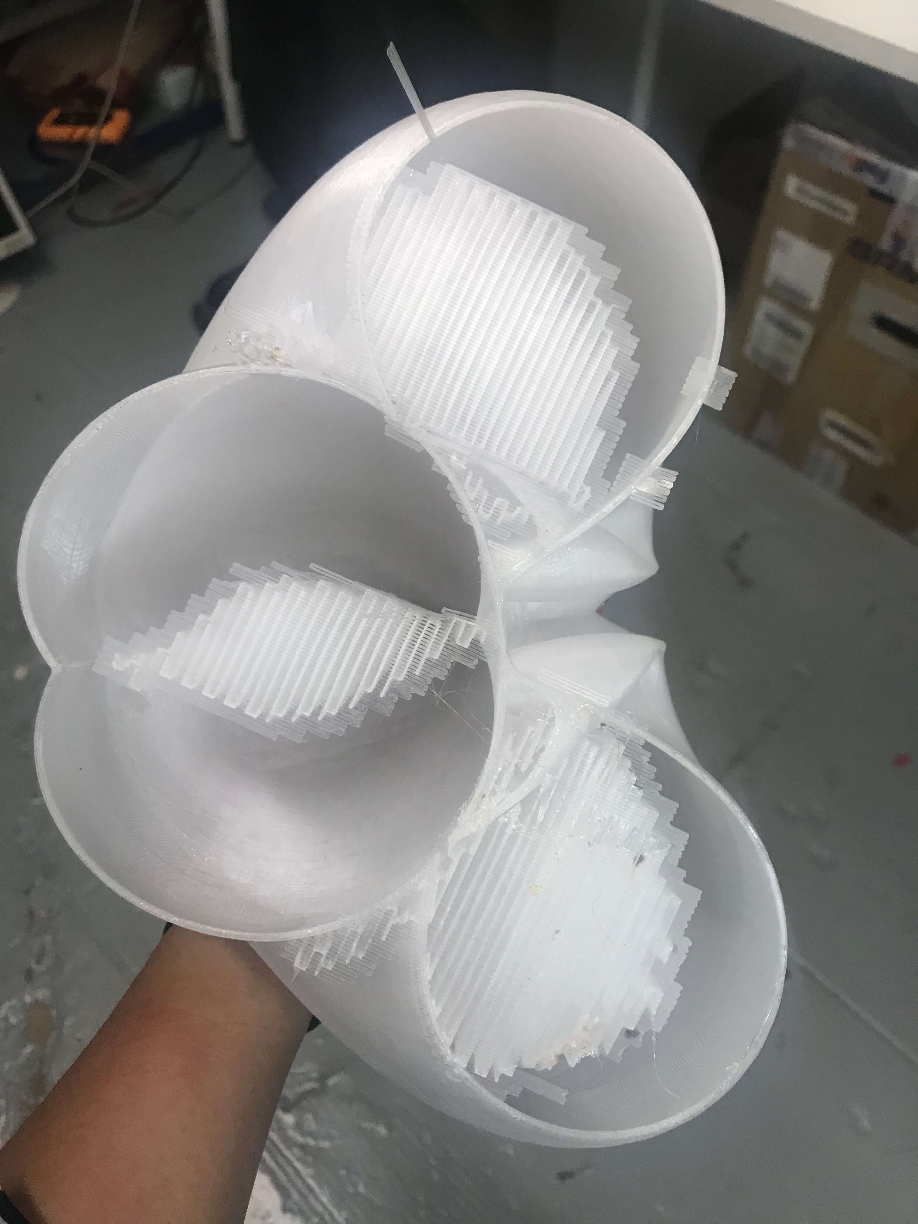
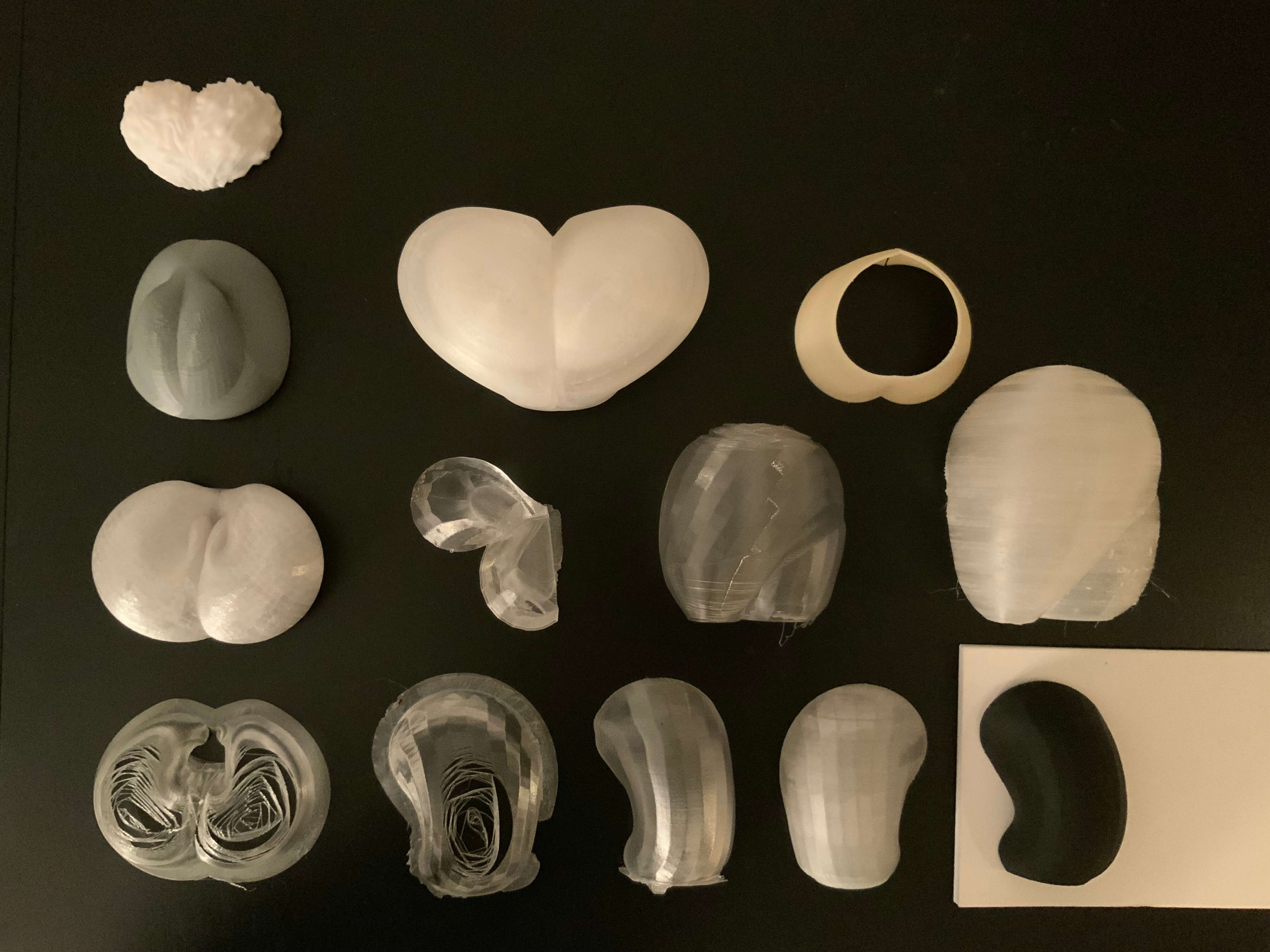
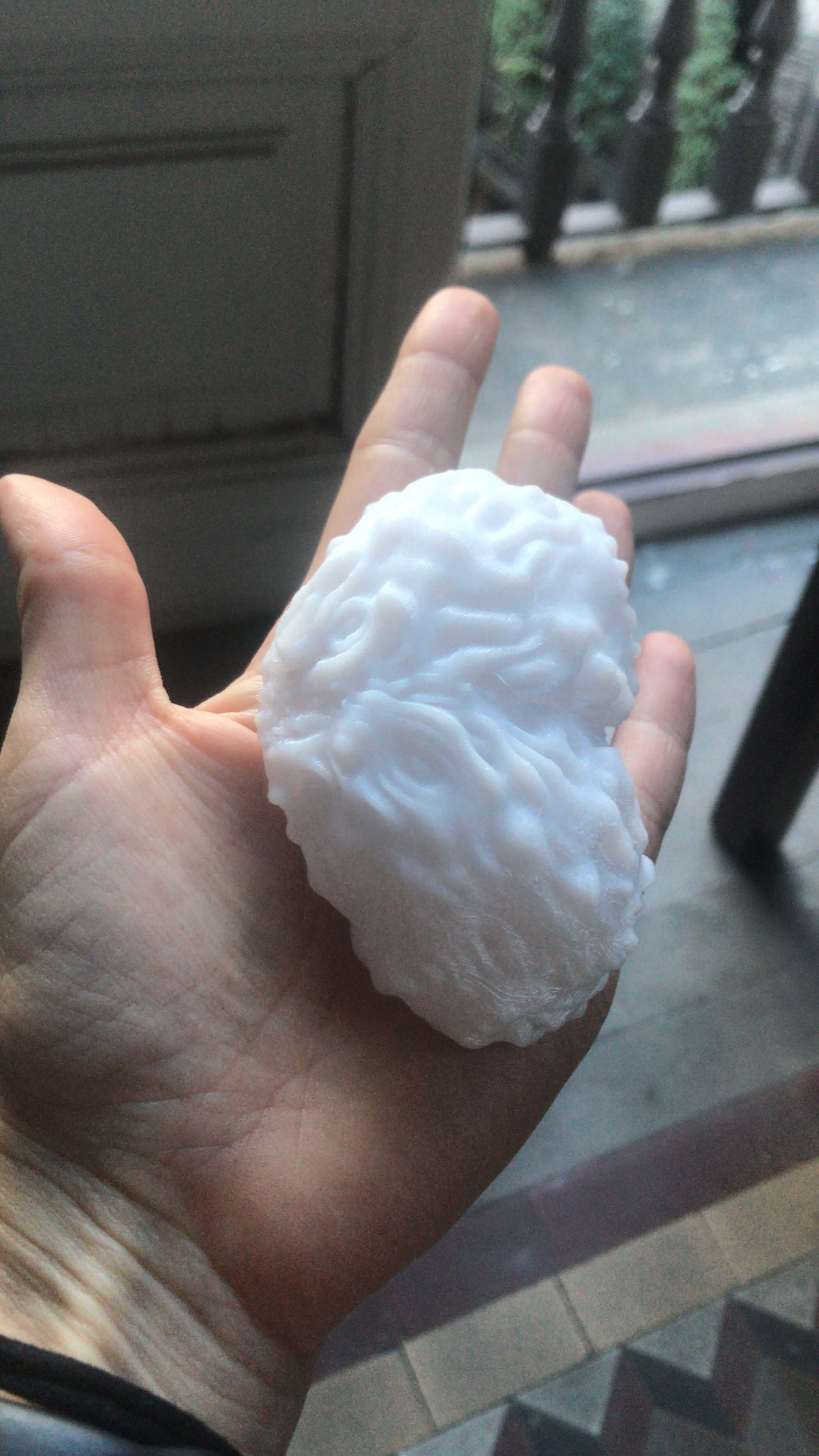
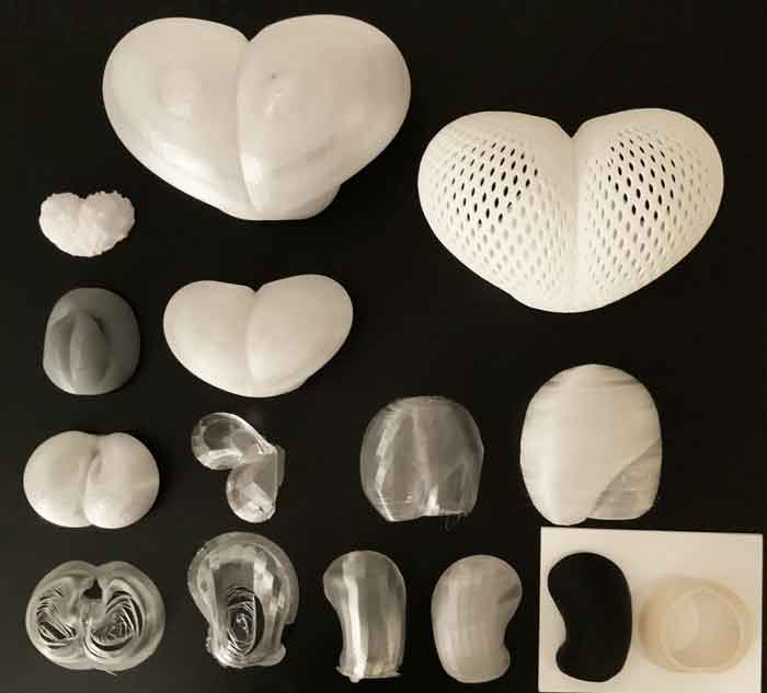
3D printed protoelements made by different 3D printers and different materials.
#test1
#test2
#test3
#test4
#test5
#test6
#test7
#test8
#test9
#test10
#test11 - print on Prusa, material PetG, printing time cca 13hrs.
#test12 - print on Prusa, material PetG, printing time cca 13hrs.
#test13 - print on Prusa, material PetG, printing time cca 13hrs.
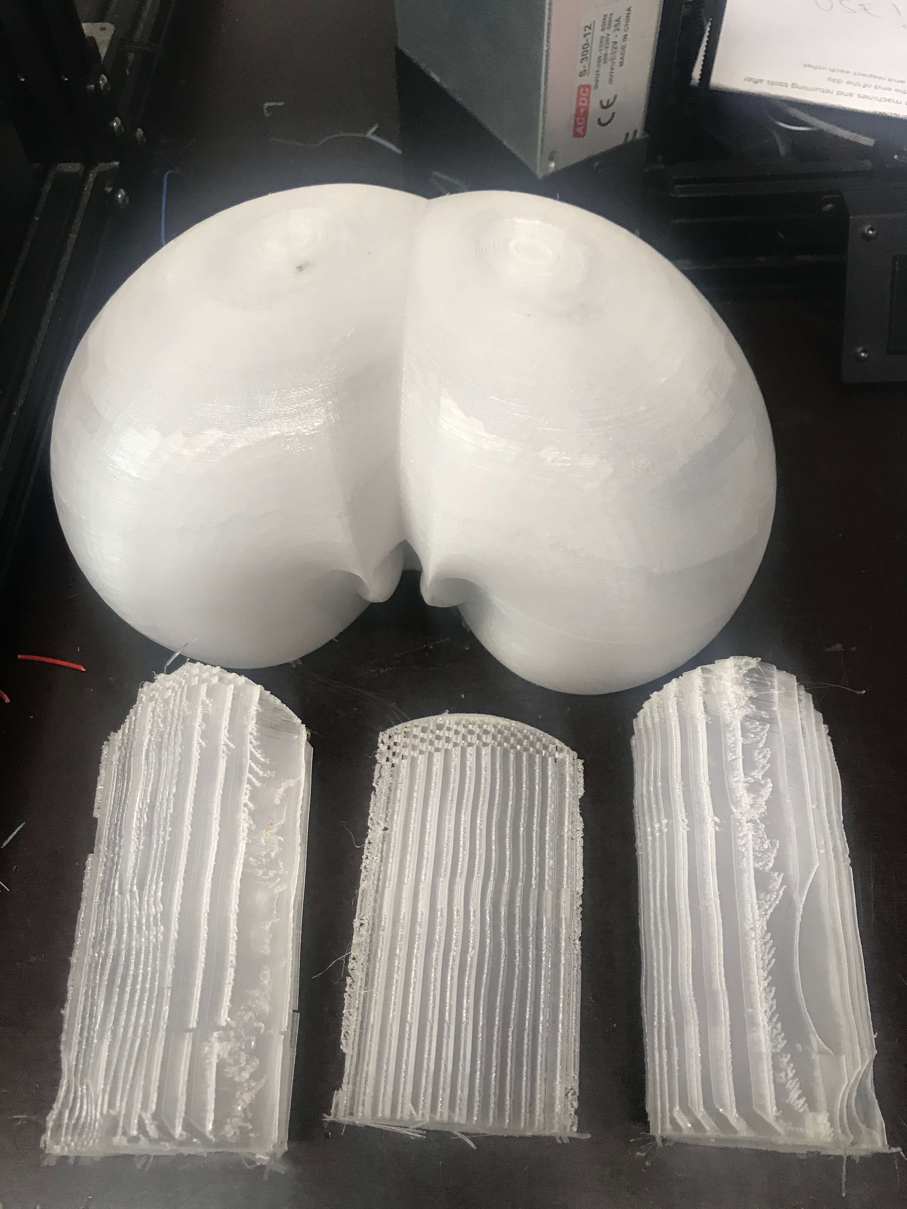
#test14 - all test prints together.
#test15 - testing new texture option. Anycubic. pla.
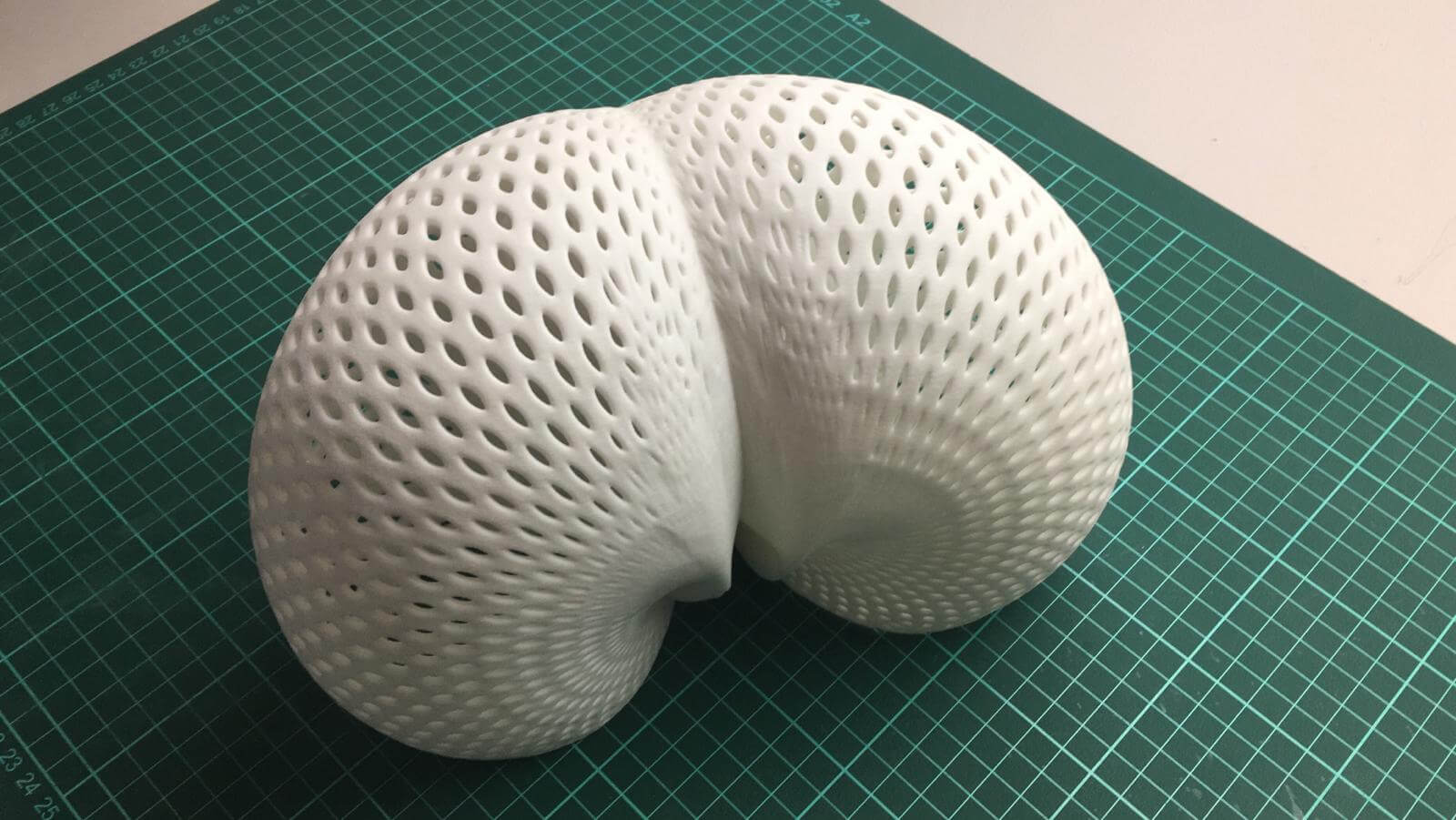
#final shell. sls.
#all prints.
#testing pattern for perforations in Grasshopper/Rhino.
#testing pattern for perforations - different stages in Grasshopper/Rhino.
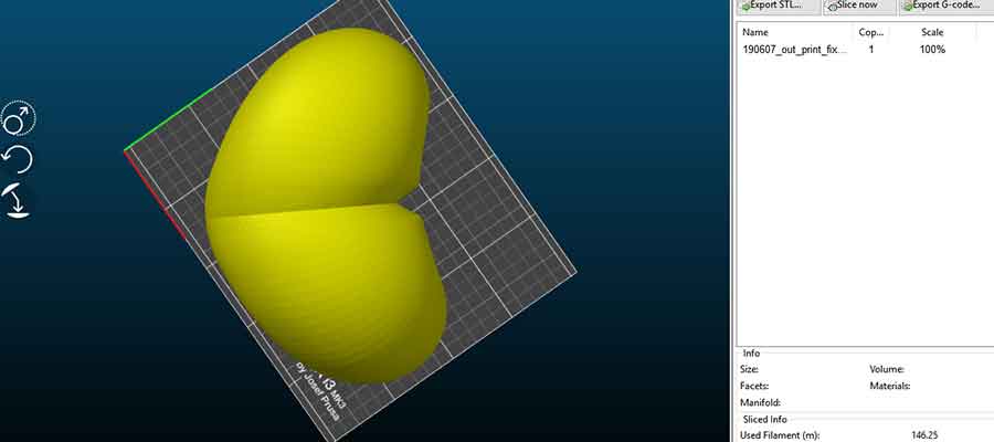
#preview of the slicer SW before printing with Prusa.
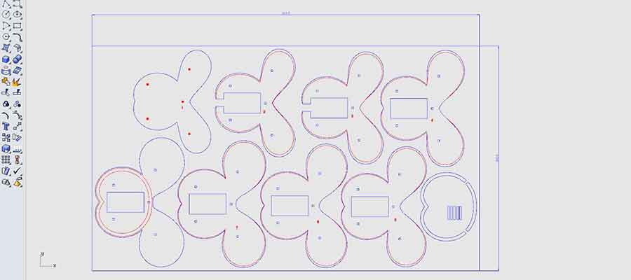
#layout of the base for lamp prototype. Rhino. the geometry was contoured according to the thickness of the material and lasercutted in wood. machine used - Trotec Speedy400.
#final perforation of the lamp. screenshot from Rhino.
#lamp base dimensions
#lamp base dimensions
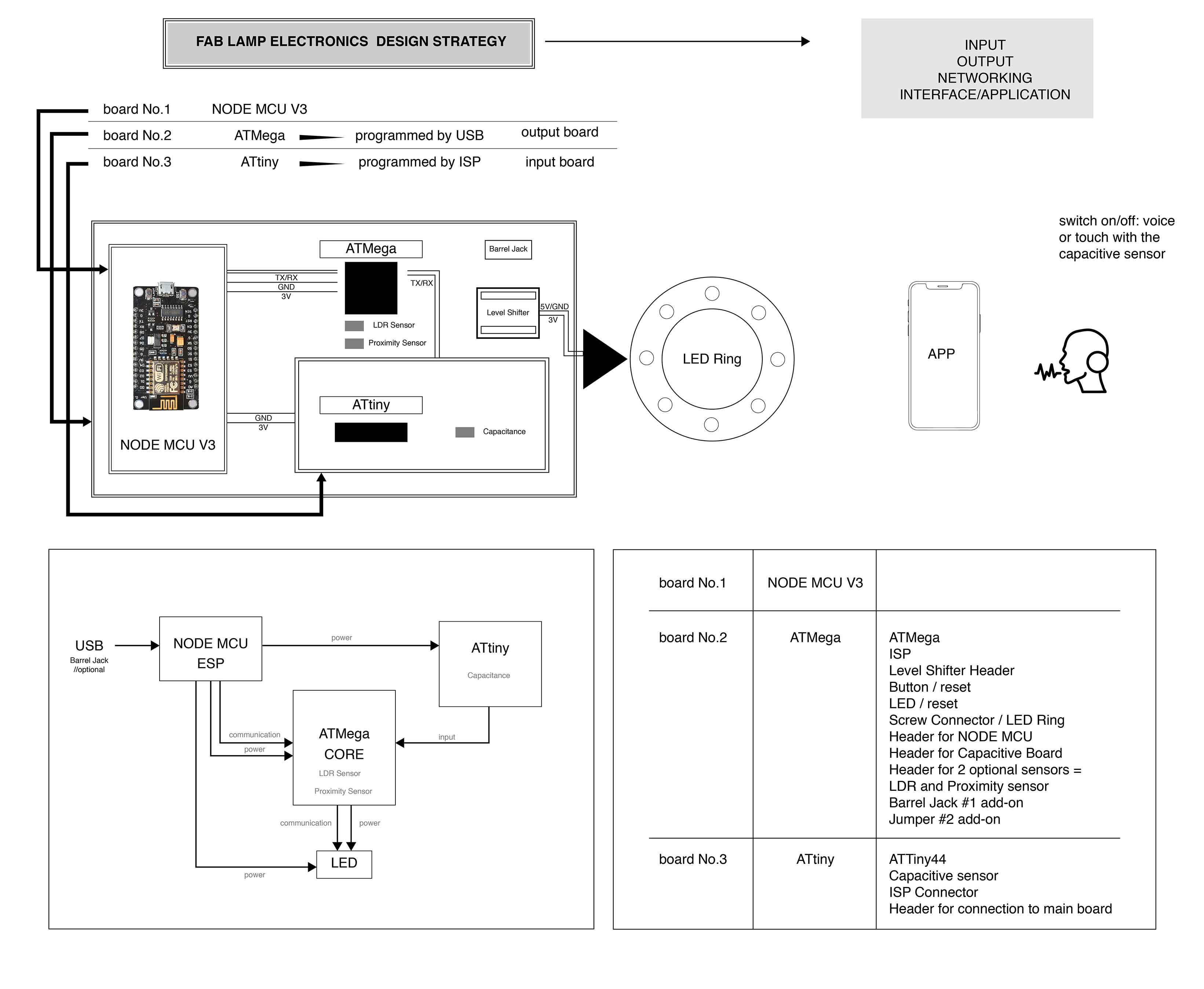
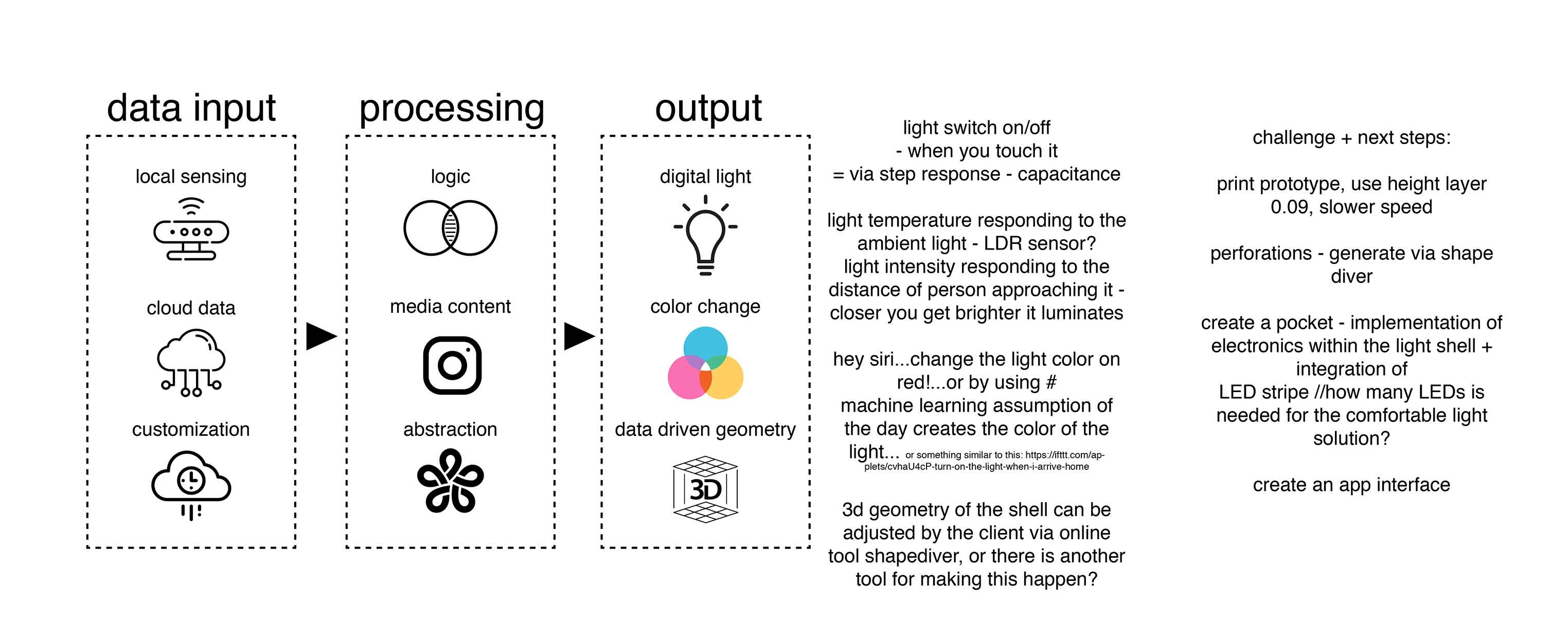
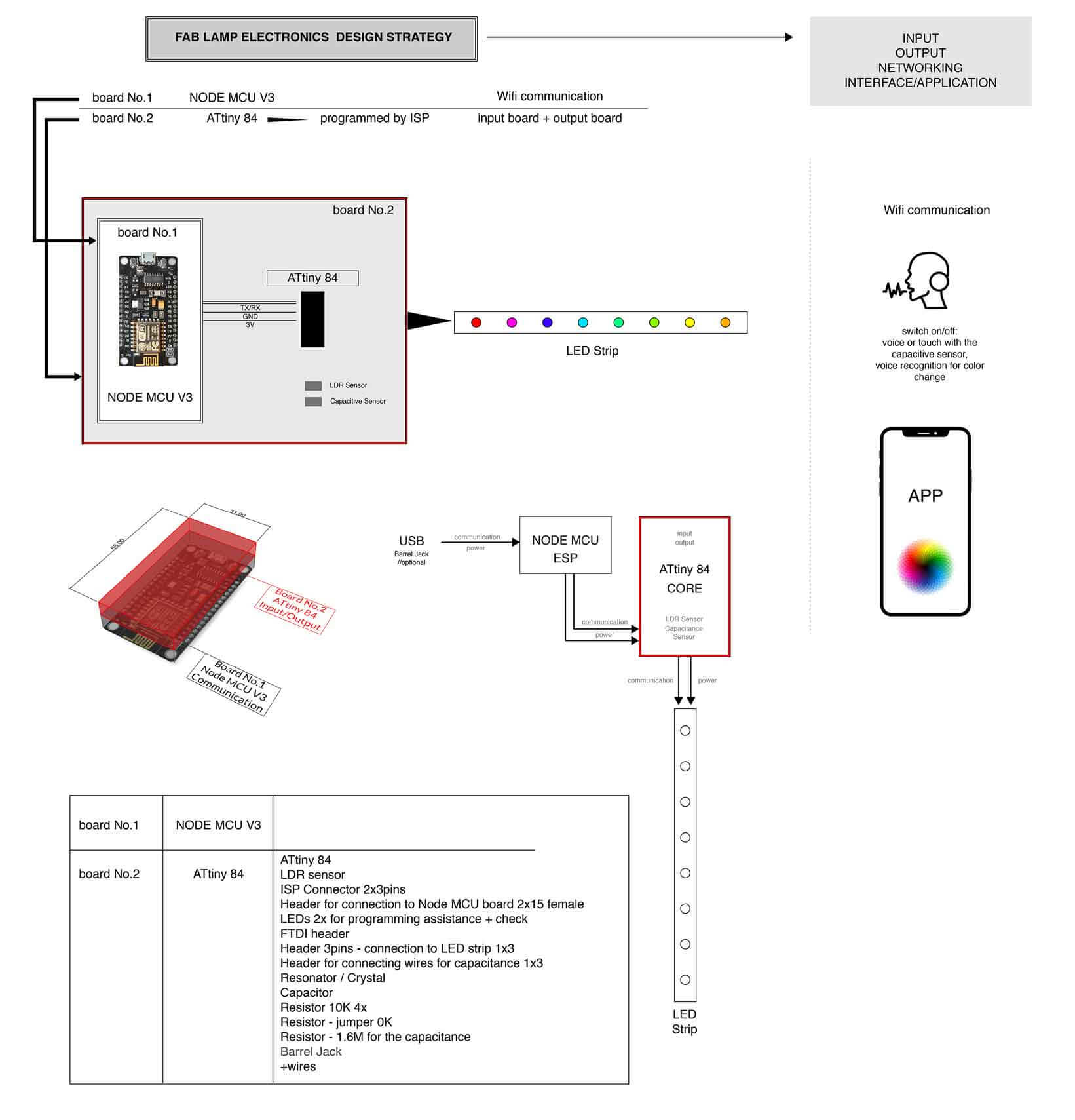
#diagram for integrated electronic systems No.1 with 3 boards. planned with the LED ring as an output light source.
#concept diagram
diagram of the whole process of electronics *created in Adobe Illustrator.
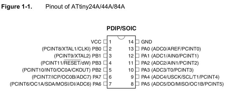
#ATtiny 84 pinout.
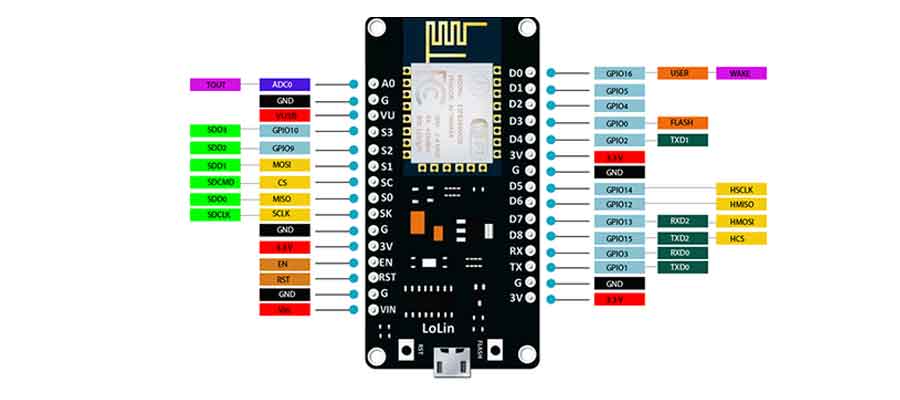
#NodeMCU v3 diagram
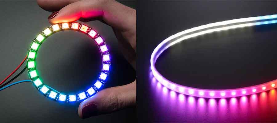
#LED Ring vs LED Stripe
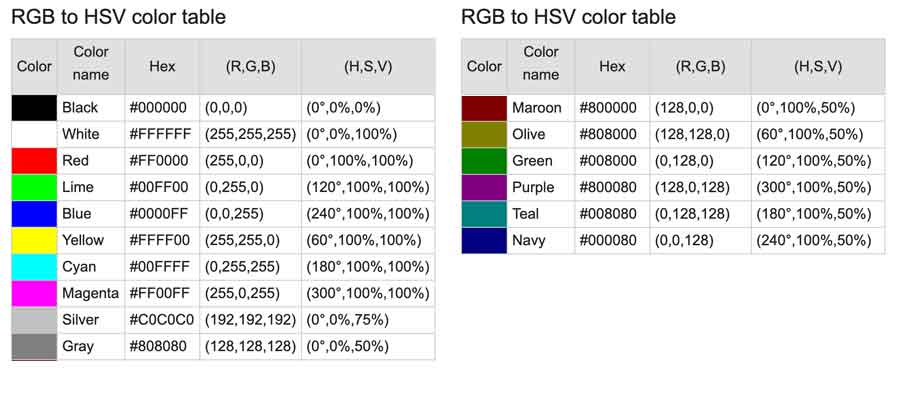
#color codes
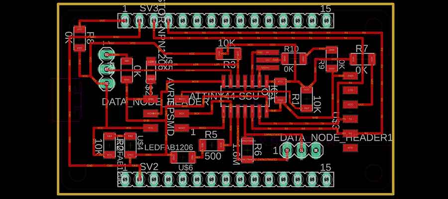
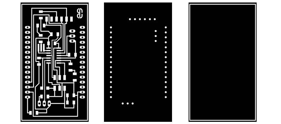
#design of the final board design. AutodeskEAGLE.
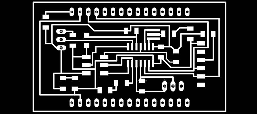
#design of the final board design. monochrome. png exported ready to be milled. AutodeskEAGLE.
#design of the final board design. monochrome. png exported ready to be milled. AutodeskEAGLE. from left to right: traces, holes, outline.
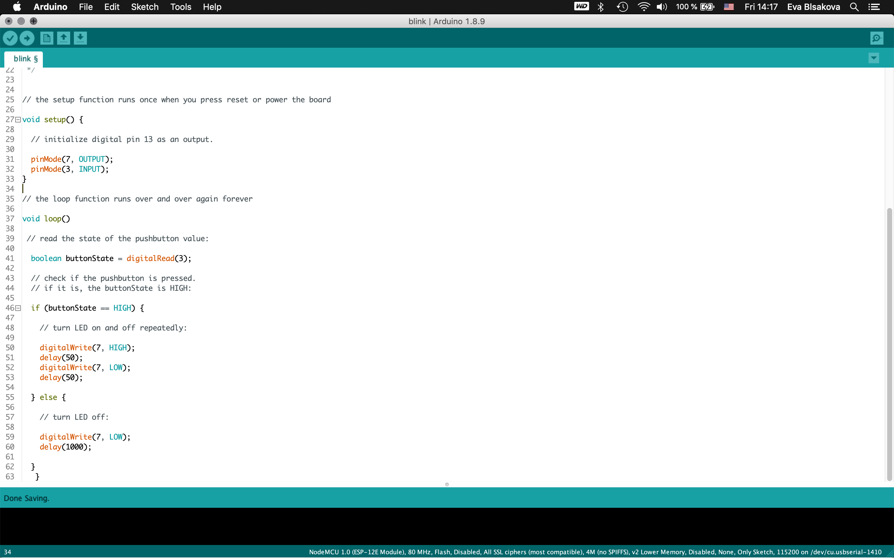
#code test library blink. Arduino.
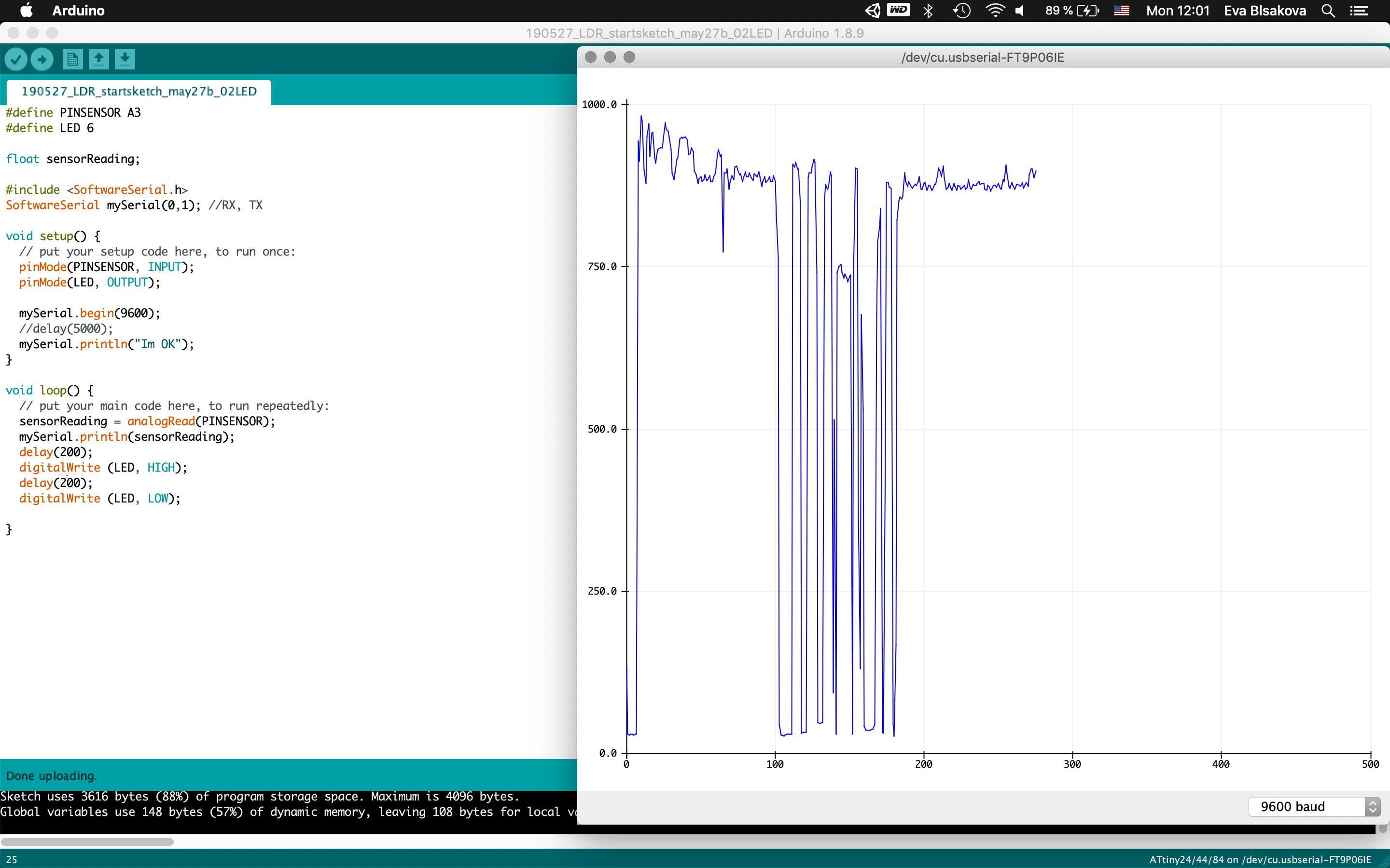
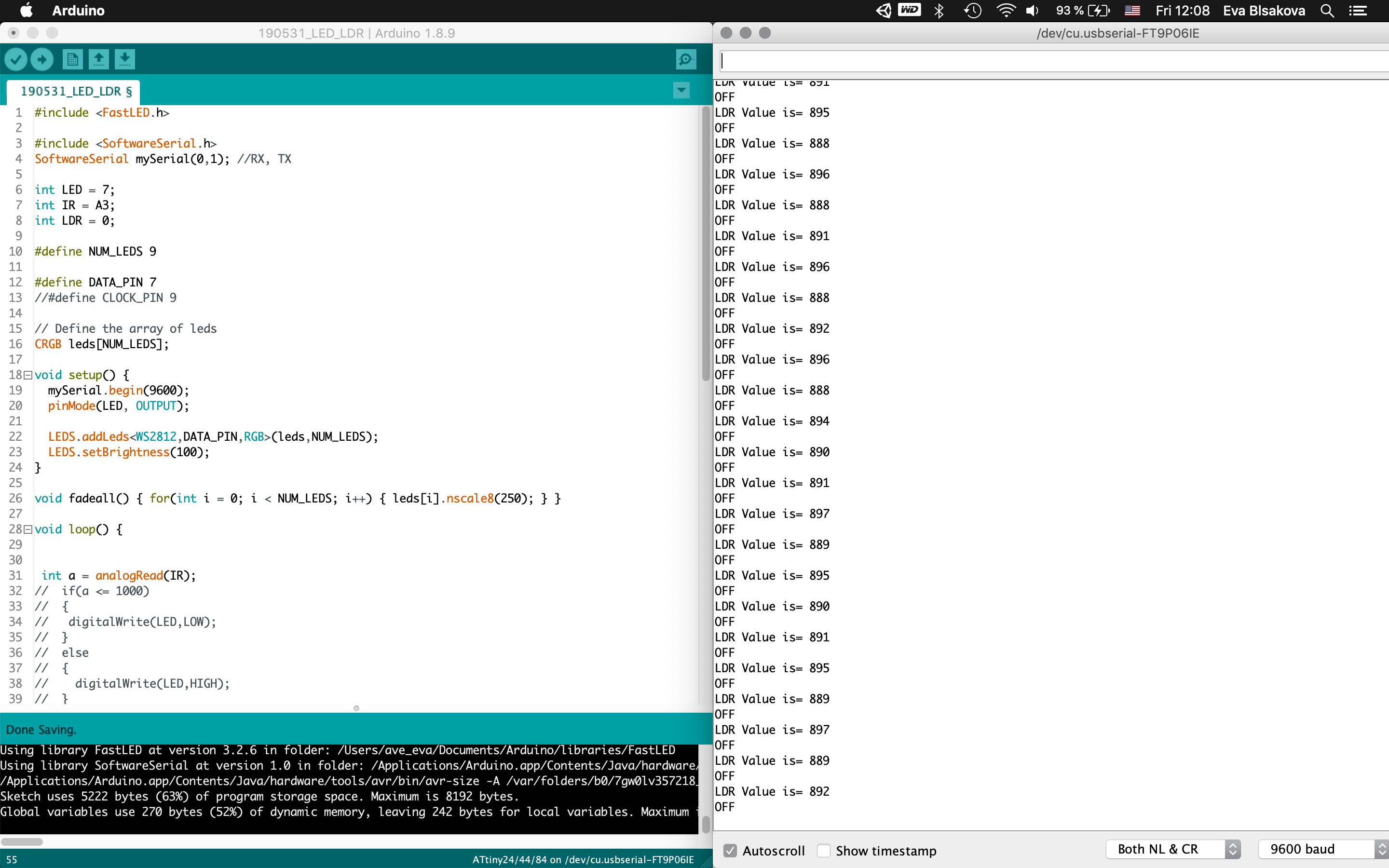
#code test - LDR sensor calibration. Arduino.
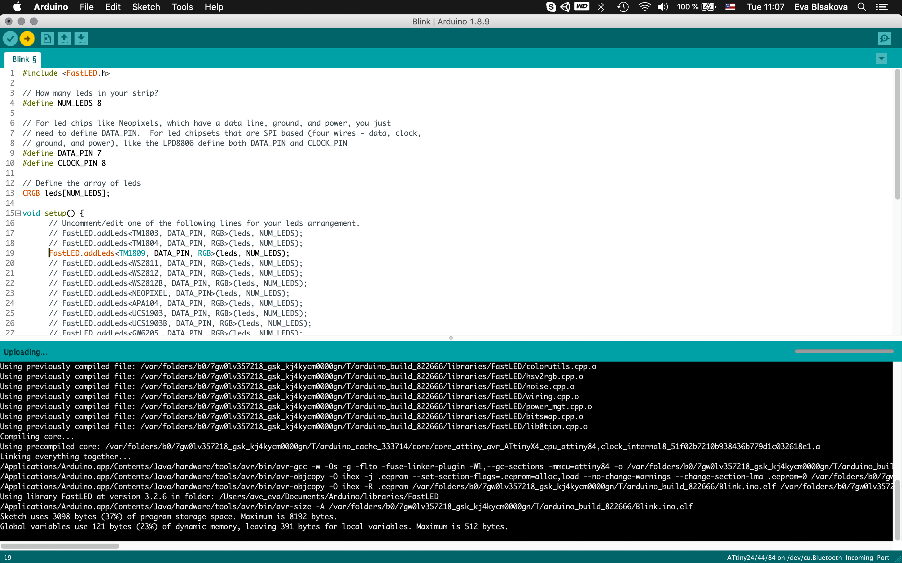
#code test fast LED. Arduino.
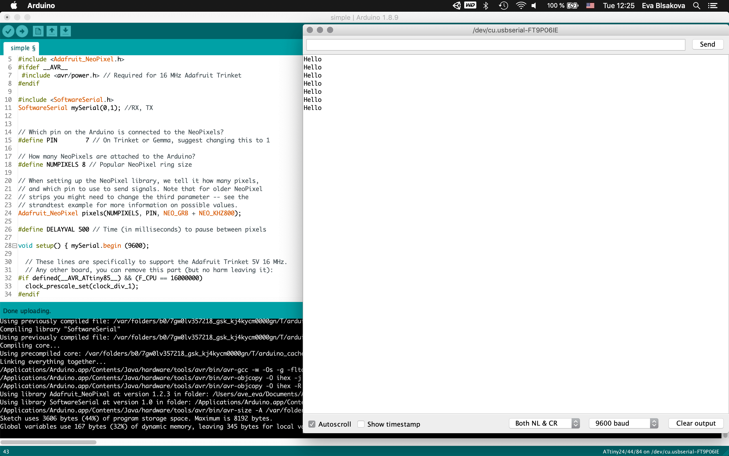
#Adafruit NeoPixel library test. Arduino.
#code test combination LED and LDR sensor and color change.
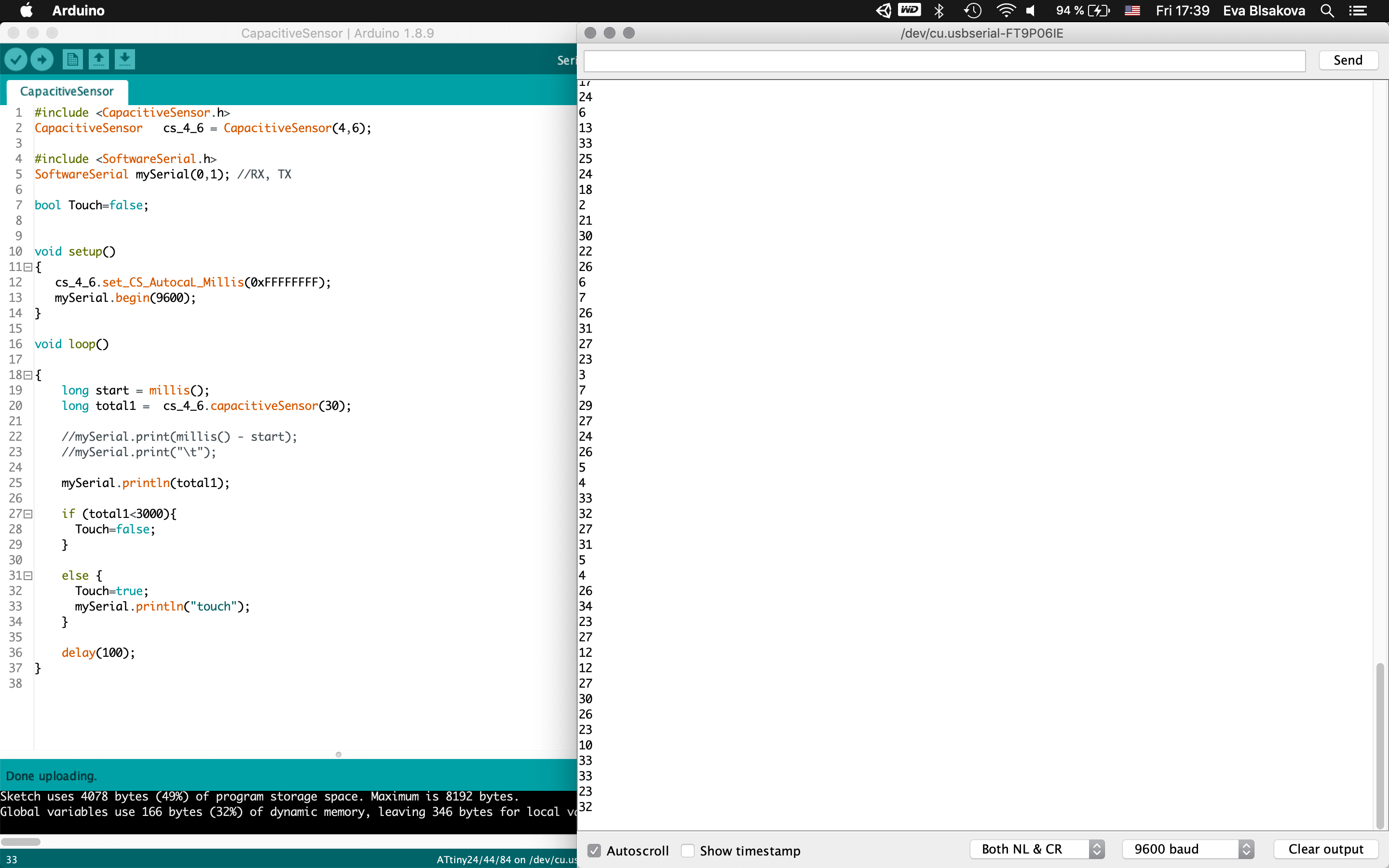
#capacitive sensor code testing.
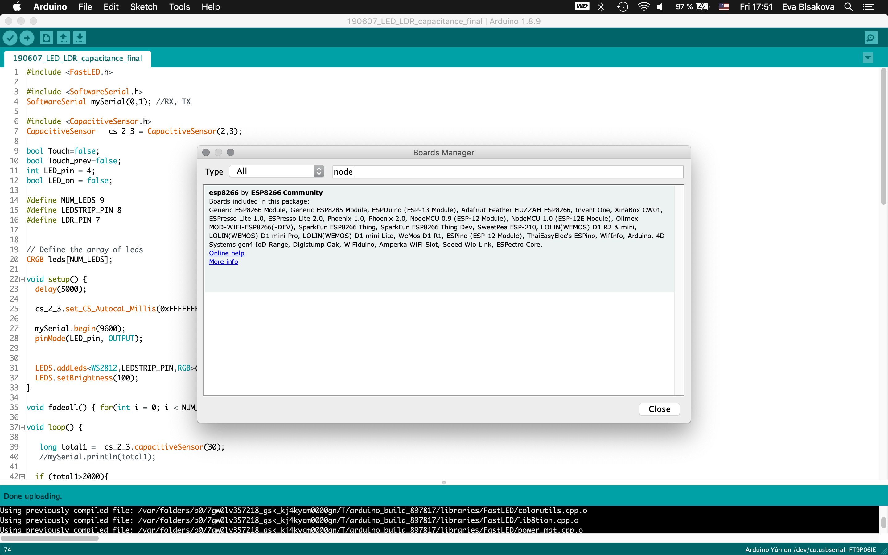
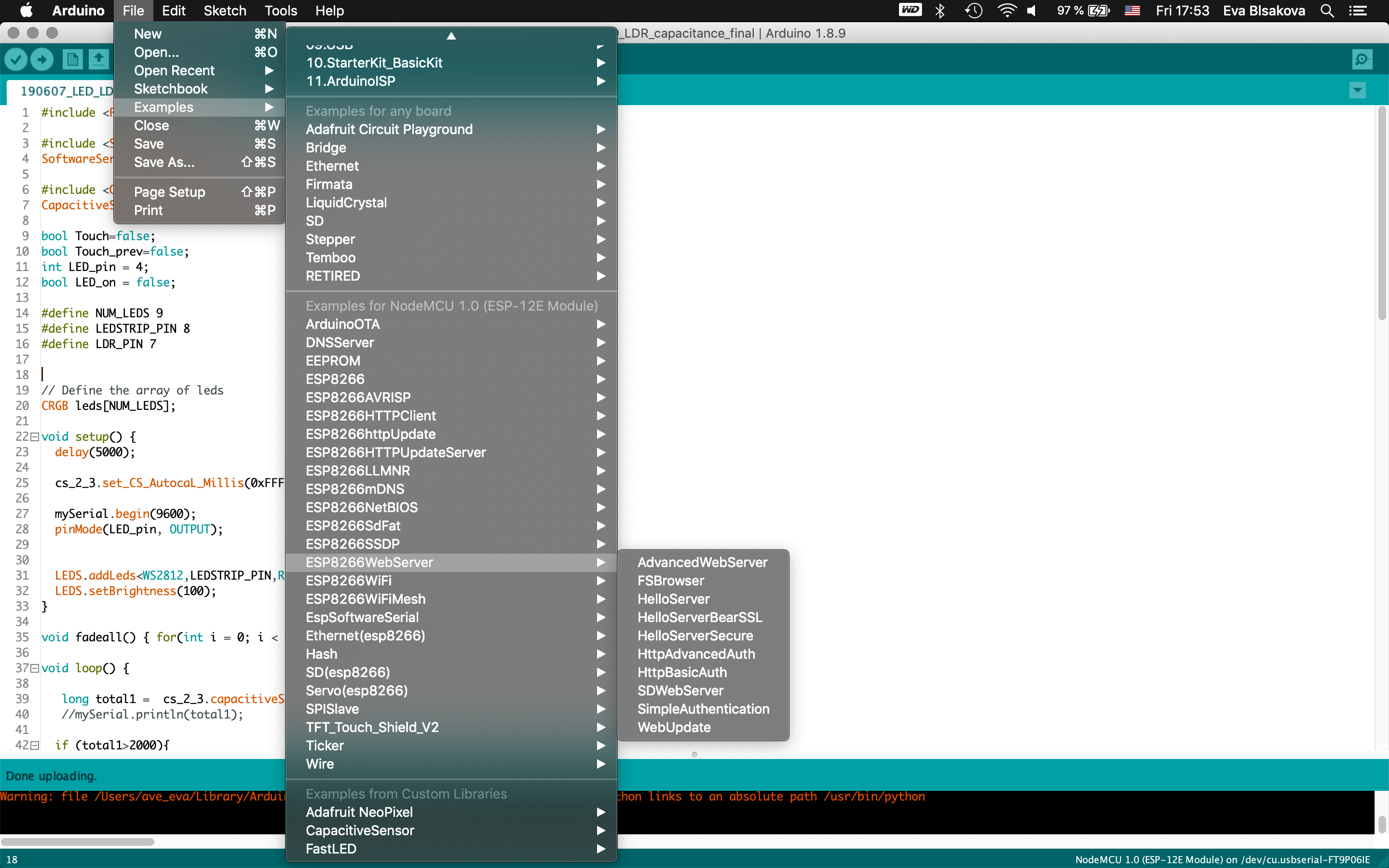
#NodeMCU linrary add in boards manager. Arduino.
#load example file to test. Arduino.
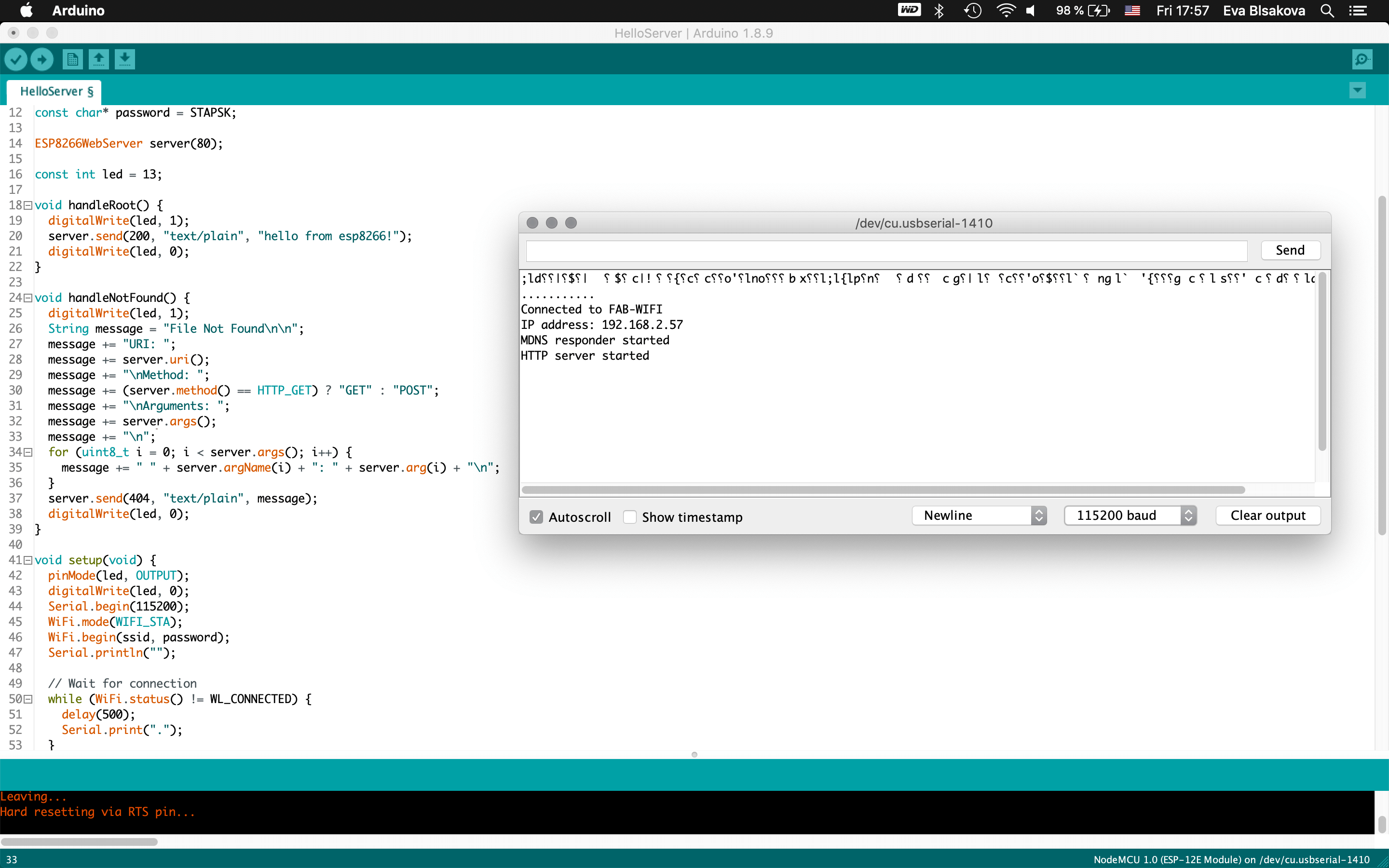
#WiFi connection check - needs to be equal.
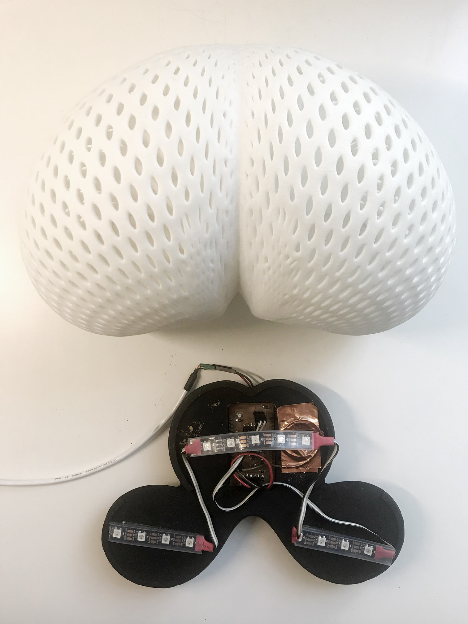
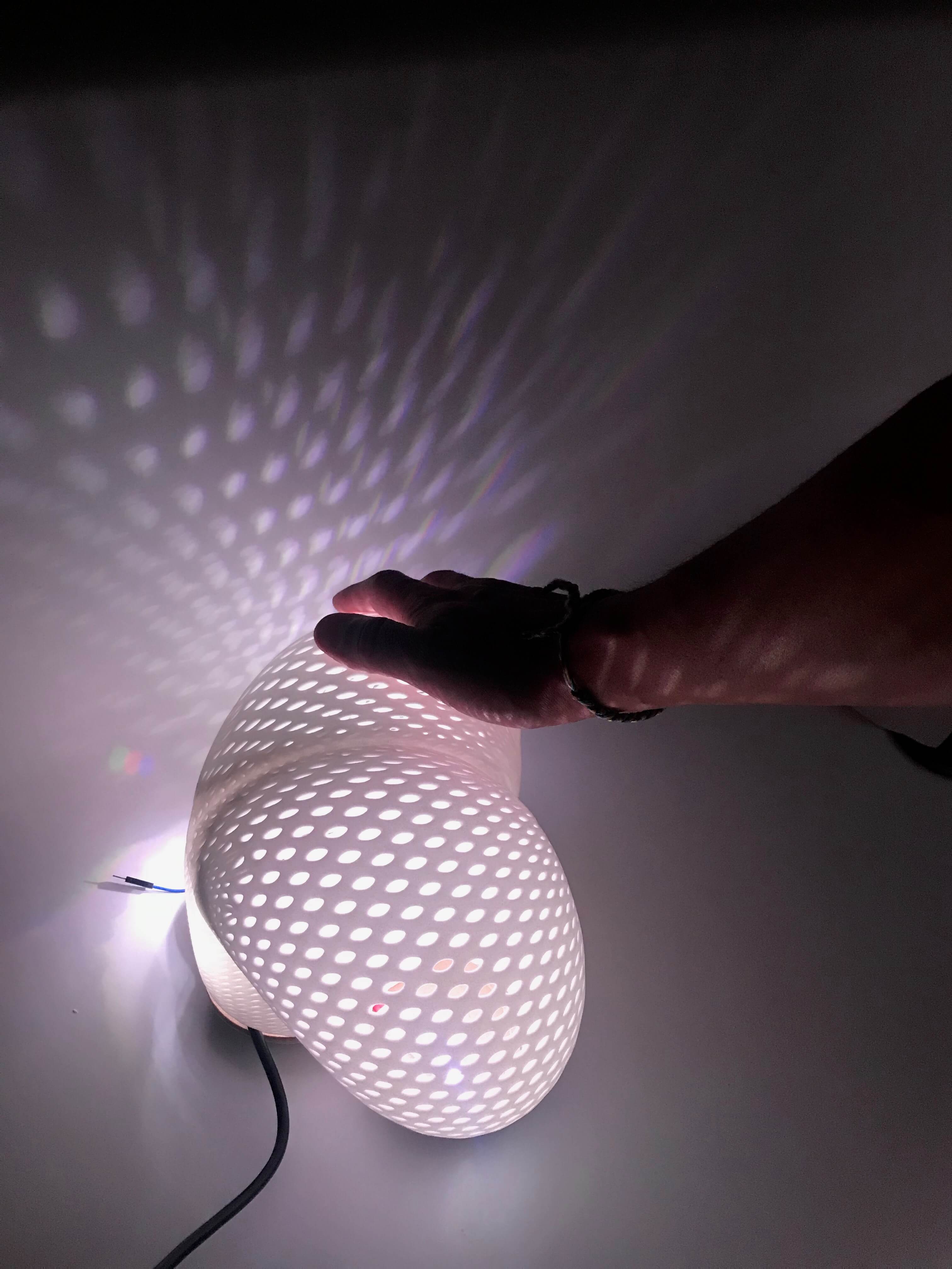
Lamp - final stage - 3d printed perforated shell and CNC milled base painted with conductive paint with integrated system of electronics - LED strip divided into 3 parts connected with wires to the central board with LDR sensor and also copper plate as a capacitance / touch sensing.
Below I am including some notes from the process(something like my fab diary)
- pt.no1 - going away from the complex attachment of LED strip *what I already tought about 3 different options how to embed the strip as you can see in the rhino folder….add screenshots after the discissuon with our instructor Xavi I made the decision to switch to LED ring - simple, easy to attach, and efficient amount of the light. e.g.:here
- add wifi input - for voice recognition app - voice to text - thunkable. here is the link with the app
- since I tried to use every weeks assignment for developing mu final project, in the week of application and interface - for this assignment I had several Ideas to work on, following my diagram I wanted to implement something like >>>Hey Siri…. something that works with the voice recognition. After discussion with our fab instructor Xavi we came up for the conclusion, that the easiest way would be to use Thunkable App Builder what is available for Android and iOS too since I am apple user and this way it would be possible. So I created a profile and dived to the exploration of the process. It was pretty easy and straightforward, the environment of the web builder is very simple and easy to use, there are many examples to follow up, you can also start with exploring tutorials. Everything works on the drag and drop system, so it's very easy.
- sound recognition using nodemcu with integrated wifi...so I created a new project for testing my device, and it was succesfull, only thing is that the system didnt recognized my voice sayin Red. so I tried to change it for the Red color, but still nothing was recognized and I havent achieved the color change to the red light color. I was always getting the error message 200 - unrecognized, and therefore the light was white.
- there is an option to download the app - download button sends you directly the link to install the app to your phone. So I have tried it, but unfortunatelly it is not trusted developer so I was not able to use it.
in the code part it was important to state some rules and connect the right API url http://192.168.2.249/TEAMSTATE=1
- struggle - 3D printing with anycubic… again fail. sh*t
- finally I managed to use prusa for the first time!!!!!!! but still the printing with multimaterial is not possible, our service and fab management is not able to fix it. sad story.
- still not sure if I will manage to print my geometry with the perforations in the lab. I managed to get a service option - outsource the print from sls somewhere else…
- preparing the geometry for robotic printing, get continuous path, boolean shell, contour geometry, think about possible solution for the top - either cut it and add separate printed tops, or add supports created from the last contours….
- what kind of material I will use? transparent? we dont have in the lab anymore…needs to be ordered…conductive? no. out of fab stock… but with thatone would be very nice to print.
- back to the electronics: - after discussion with instructors decision to make a HelloBoard /attiny microchip with LDR sensor - this could work as a prototype - how to connect this to the NodeMCU and ATMega?
- HelloBoard_LDR - eagle - how to connect it with the header component, which pins, where? and why? what else is needed to add? and how to connect it to the rest?
- laser cutted bottom part with integrated electronics - for the small prototype as a proof of the concept use a vertical placement of electronics
- I finnished eagle board - simple board - hello light board with LDR sensor. I received the package with milling bits, boards and microchips, (this is a new upgrade because 3 years ago we didnt have this) so at the end we managed to start with the milling of the traces, ok, this was good, worked out…I just broke the milling bit at the end when I wanted to move the axes and instead I pressed Y not Z…lukyly I had the traces already milled. next step was to make a holes, so I changed the milling bit to 1/32. so I loaded the file and it seems to be correct, just it was milling in the air, so it seems to have the problem in the file, I need to repeat the loading of the file in the MODs and save it again.
- than it worked...so to sum up - milling the board, checking where are the bits, finding the right components, soldering it to the board,…
- today printing this file: 190525_out_print_0.8offset_fixed.stl - not really progressing with the printer, has somehow broken sd card reader, gonna try tmrw…
had great talk with diego about my lamp, he suggested some interesting ideas like giving meaning to the color change - create a value for it,
Science of color
inspiration e.g. : bees can bees be trained to heal cancer
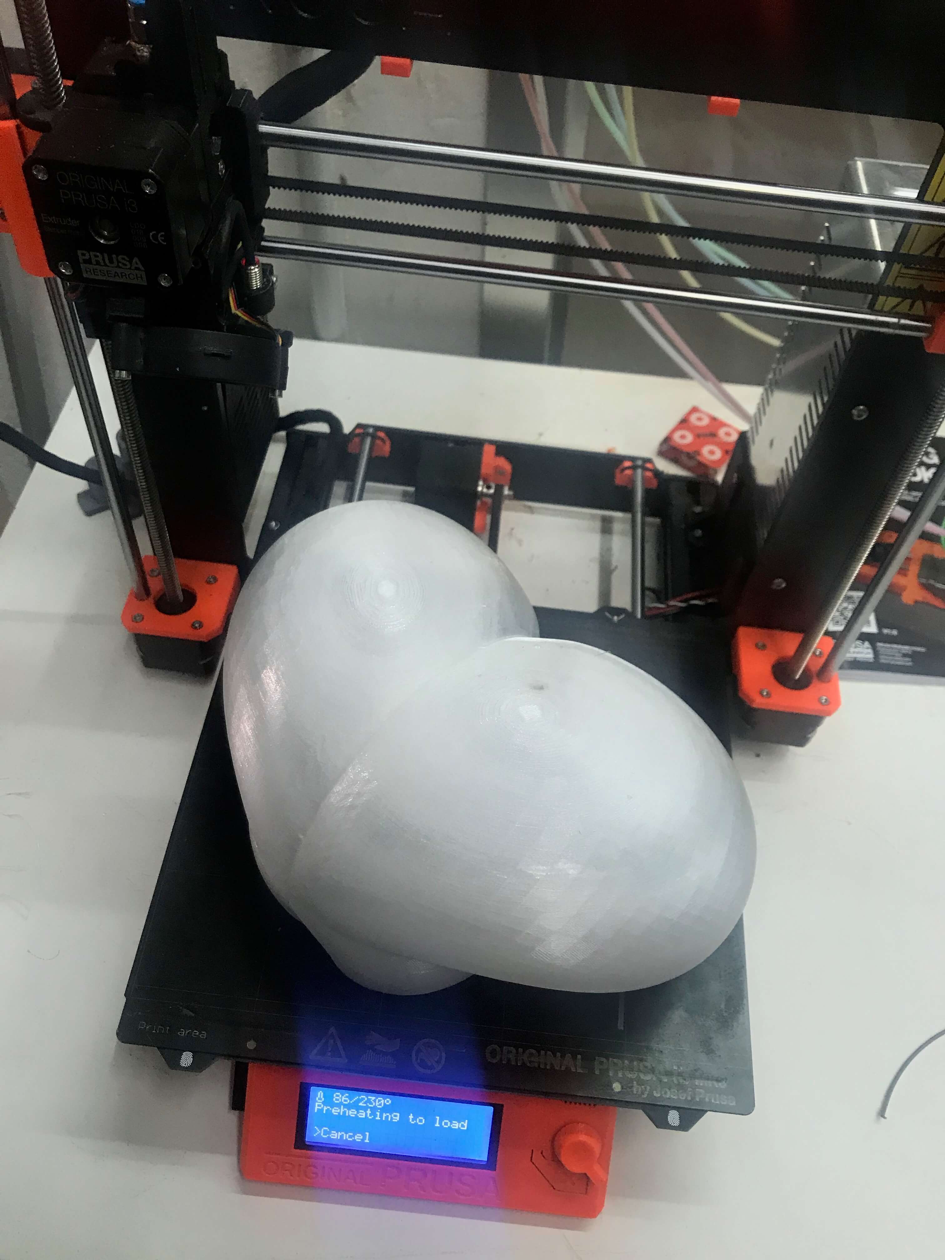
- I printed my shell file. on zortrax. with zglass material. now it worked… there were some traces - net from the material, improvement could be the adjustments of retraction but unfortunatelly on zortrax is not really possible, solution is to print it with 0.09mm height as Raffa said…I printed with zortrax printer and material zglass
- today - programming the board, with attiny44 was not working so I resoldered the new chip to attiny84 and tried to download the neopixel libraries. I tried to follow this http://fab.academany.org/2018/labs/barcelona/students/joris-navarro/classes/09--embedded-programming/
was not working.
- serial is not working in tiny chips, instead use mySerial and
#include
SoftwareSerial mySerial(0,1); //RX, TX
but go for mySoftwareSerial while using ATtiny84
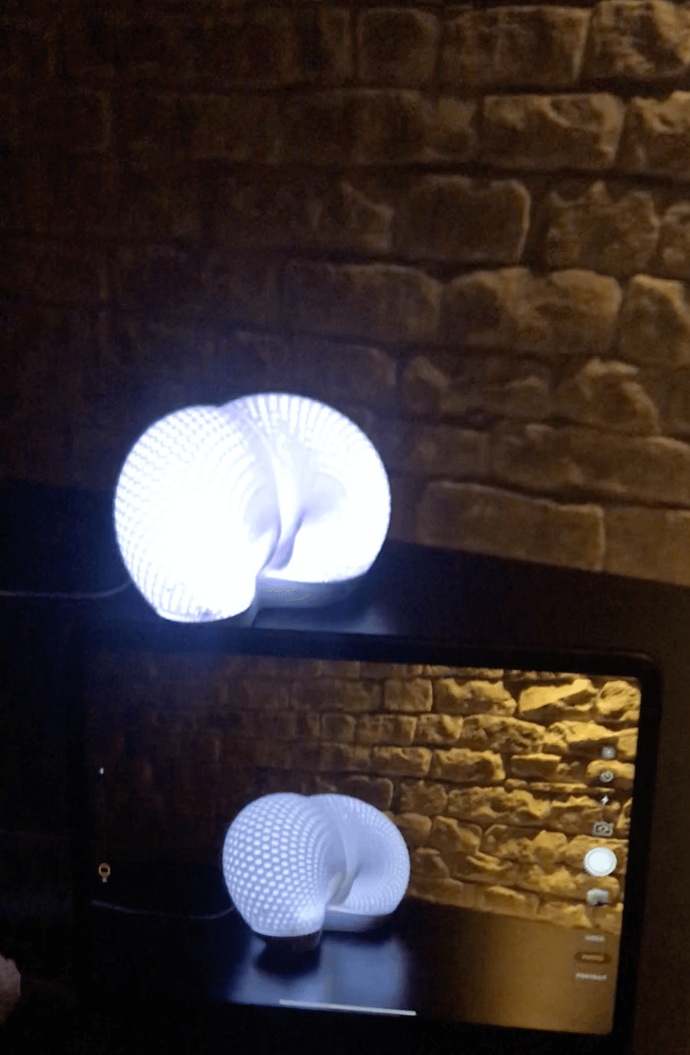
- project description text 1.0: concept is an interesting way of adding some light to your home. FabLux lamp is perfectly disguised on your table while hiding it’s LED secrets from view. The installations conceal LED lights, and from its appearence the form looks like a heart…look like you’ve got some kind of weird space-time holes into your walls and leaking light into your room. Painted with the same color as your walls. In conclusion if you want an original way to add light to your walls then FabLux Lamp might give you a FRESH idea! just say it to your phone and choose a color u want!
- rescaling the final geometry and getting the new podest - laser cutting the base
- I got the conductive paint and with that I would like to test it on my lamp with capacitance.
I followed this link with explanation how it works:
https://www.bareconductive.com/make/diluting-electric-paint/
- the presenation slide and video done, presentation slide in illustrator/in design, and video in iMovie, after I compressed the size of it in here: https://www.mp4compress.com
- now I am tryin to make a PCB for my final project, it will be a shield to NodeMCUv3. I struggled to search and import an existing dxf or svg to eagle… than I downloaded 3d model
from here
https://grabcad.com/library/lolin-nodemcu-esp8266-development-board-v3-1
and imported it to rhino>make2d and than import to eagle. it is hard to move it to my area of working…
PCB - final project:
check the necessity of FTDI
check the pins for capacitance + resistor
milled the board…final board… I had to mill it 3 times - 1st, the outline was not correct, 2nd - the platform was wobbly and it didnt cut the paths properly, so 3rd time I switched for another machine and than it worked!
soldering of final board, programming/burn bootloader it and uploading the code - start with final code adjustments
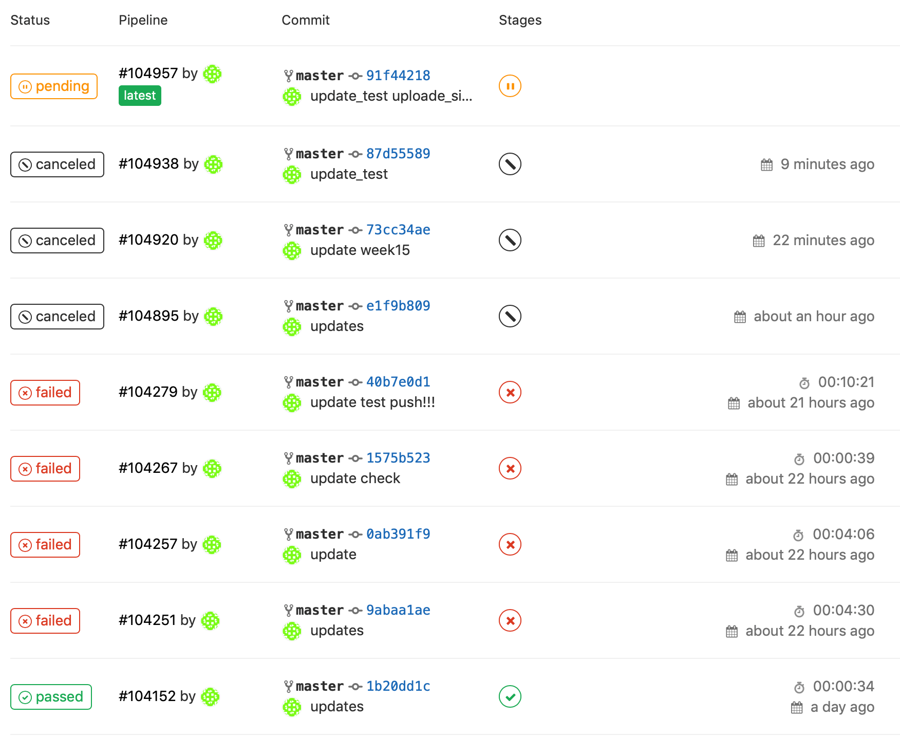
- once I started uploading all my content to the repository, there was a moment when I was not able to push the content from my comp online...why? the issue was too large file size (when I placed the .stl of the final project files for 3d printing) till the time that I was not able to do so anymore, because I put to my web repository files to upload for downloading, to final project part I placed my stl files, they were just too big that it crashes my pushing process… it was needed to check what was the issue, so checking the gitlab link (pipeline) after logging in to my account:
it looked like that. But of course I resolved this issue and you now you can enjoy all of this on my website.