Week 6. Electronic design
During this week I designed, fabricated and tested a basic board for the ATtiny44 from scratch.

Tasks
- Redraw the echo hello-world board, adding at least one button and a LED
- Fabricate the board
- Test the board
- Measure its operation
Process explanation
Design a Hello-World board using Eagle
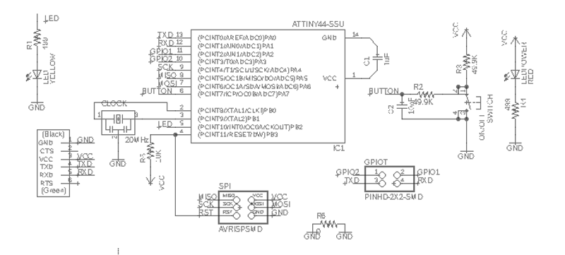
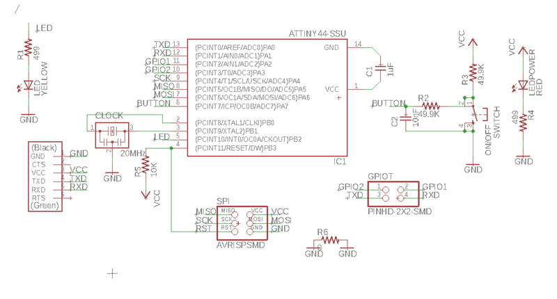
I decided to create a board utilizing the Hello World FTDI as an example (Figure 1). I decided to use Autodesk Eagle as a EDA (Electronic design automation) to design my board. It is one of the most utilized tool for the hobbyists all around the world. In the future I might try other alternatives. My board should include in addition to the previous components:
- A Green LED programmable from the ATTiny
- A button with a simple debouncing circuit (that is, to avoid glitches in the transitions)
- A RED LED indicating the circuit is powered
- A set of extra headers connected to free pins in order to connect external sensor and actuators. The TX and RX signals of the FDTI will be utilized when not in use it for programming/using serial port.

The lists of components to use are:
- Atmel ATtiny44 microcontroller
- 20Mhz Crystal
- SPI headers pins
- FTDI header pins
- Pull up resistor for RESET signal (10K)
- Decoupling capacitor: 1uF
- Omron switch
- Debouncing circuit: two resistors of 49.9k and one Capacitor of 1nF
- Yellow programmable LED + its current limiting resistor (499)
- Red power LED + its current limiting resistor (499)
- 6 pins header (SPI MISO, SPI MOSI, FTDI TX, FTDI RX, 2 pins free left from ATtiny)
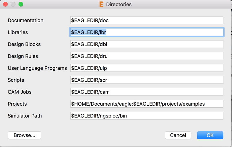
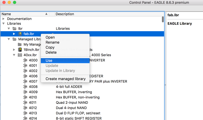
I installed Autodesk Eagle 8.6.3 in my mac machine. Next, I had to install the Fab Lab components library ( fab.lbr ) containing majority of components from the Fabinventory . I just downloaded the library and placed in the "library folder" of my Eagle installation. Actually, you can set where Eagle looks for your personal libraries in Options>Directories. Finally, in order to be able to to use the library, I should select it on the left menu, click with the right button and select Use. Other option is to click on the gray button located at the right of the library name.
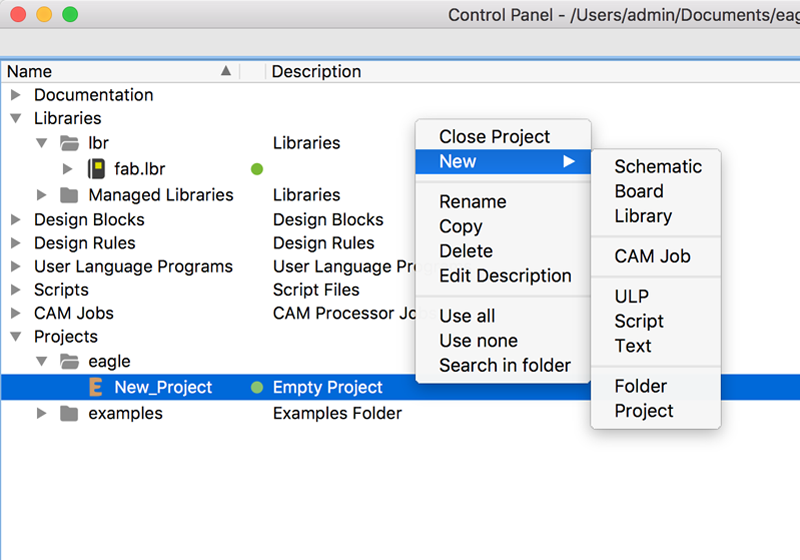
After creating a new project File>New>Project, I need to create the schematics: Put the mouse on the new created project> Right button>New>SchematicA schematic diagram, is a representation of the components of a circuit using graphic symbols (simple shapes). It shows also the lines which connects the components and through which the electricity flow. Figure 4 shows the main buttons of the UI. When you press the button Add componentyou select a component from the libraries in use to be added to the schematics. In order to simplify the search of components (reduce the number of options) i marked as used just the fab.lbr and the supply1.lbr. I marked the rest as not used by clicking on the green button.
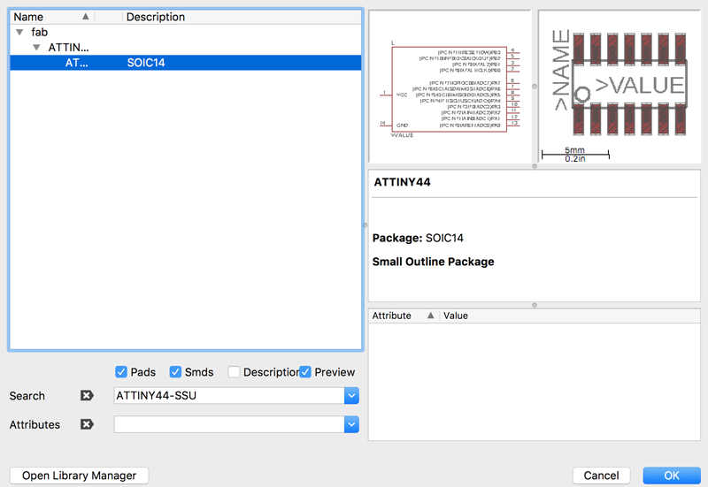
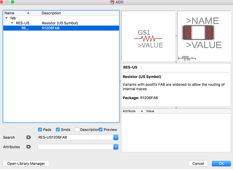
When you add a component (using the Add component button) is very important that you choose adequate encapsulation. We are not using throughhole components but surface mounted ones, so we must be sure that we select that encapsulation. Usually, components in the fab inventory contains the FAB suffix somewhere. When you add a component (press Enter button when you have selected the correct component), the ADD window opens again. If you want to remove this window just press ESC button. If you cannot find the adequate component, you can use the Search button.
If you want to move a component, just press the Move button from the Menu and click on the cross located inside the component you desire to move. If you want to rotate a component, select a component using the Move tool and press the right button of the mouse.
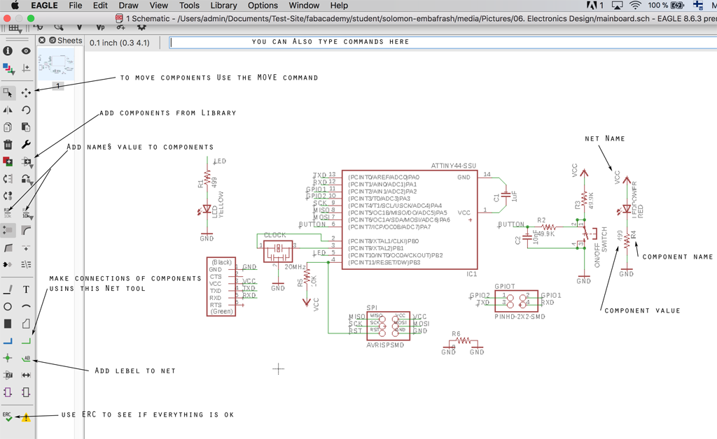
I added all the components and give them adequate Name and Value using the buttons on the Menu. The name is the reference name of the component (e.g. R1) while the value is the real value of the component. For the components that does not have a value (e.g. LED) you must add a significant characteristic (e.g. color of the LED).
After that you must create the connections among the components. To that end, I used theNet tool and NOT the wire/linetool. In order to simplify the circuit I gave names to some of those Nets using the Name tool. Two netswith the same value will be linked in the board file (they belong to the same electrical line). In order to visualize the name of the nets use the Label button.
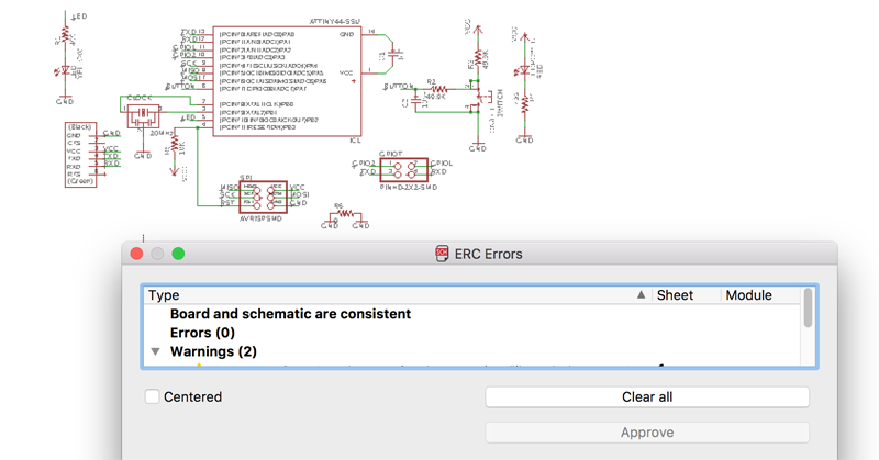
After creating all the connections, I run the ERC (Electrical Rule Check) to check that there are no problems with the signals. I got two warnings (Figure 8), but they were caused by the way I drew the circuit. After the schematics was correct I moved to the board view pressing the button Generate/switch to board view. This view permits drawing the traces for the circuit. The main tools I utilized are shown in Figure 9.
I made sure that the traces had the correct size. We are using a milling bit of 1/64. We have to be sure that the isolation lines are of the correct size. Considering that we are using several offsets of 50% we cannot choose a width for the line much smaller than the milling bit. Hence, I thougth that 0.015 mils was a good size. Go Settings>Widthand be sure that it is marked 0.016. You can move the components using the Move button. I placed all the components in my candidate initial position before starting any traces. I had to move from the schematics to the board view several times in order to check the names of the components. I finally opted to print the schematics in paper to make my life easier.
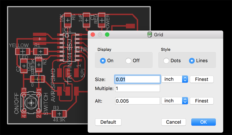
I created manually all routes using the Route button. However, before starting the manual work I pressed the Ratnest button. This button calculate the shortest airwire for the current position of all the components. Once you are drawing a route you can select multiple wire bends (straight angle, non-straight angle, linear, round ... They are quite helpful in order to draw adequate lines. By default, Eagle use a snap grid to place the routes. You can define the grid size pressing the Grid button. In addition, by pressing Alt while creating the route you can define a finer position. You can also set up the Alt resolution in the Grid tool(Figure 10). For some routes I had to set the grid to 0.025 inches with an Alt resolution of 0.005 inches.
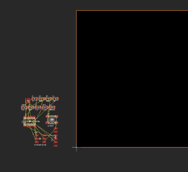
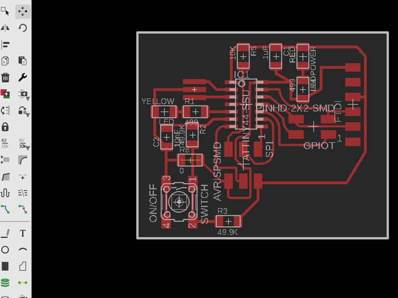
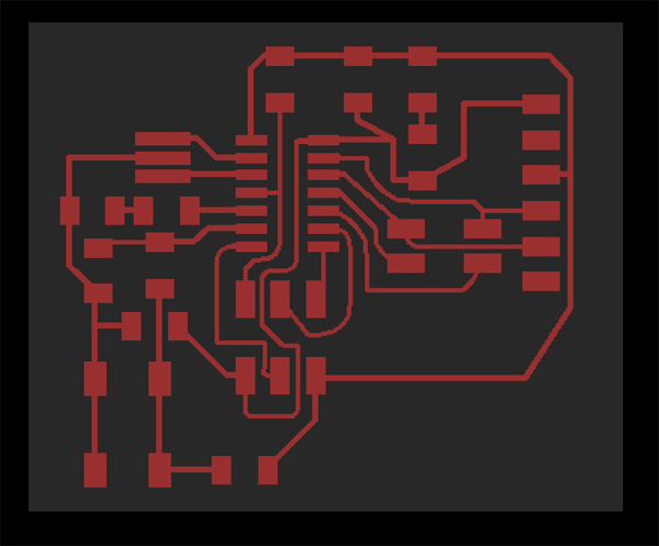
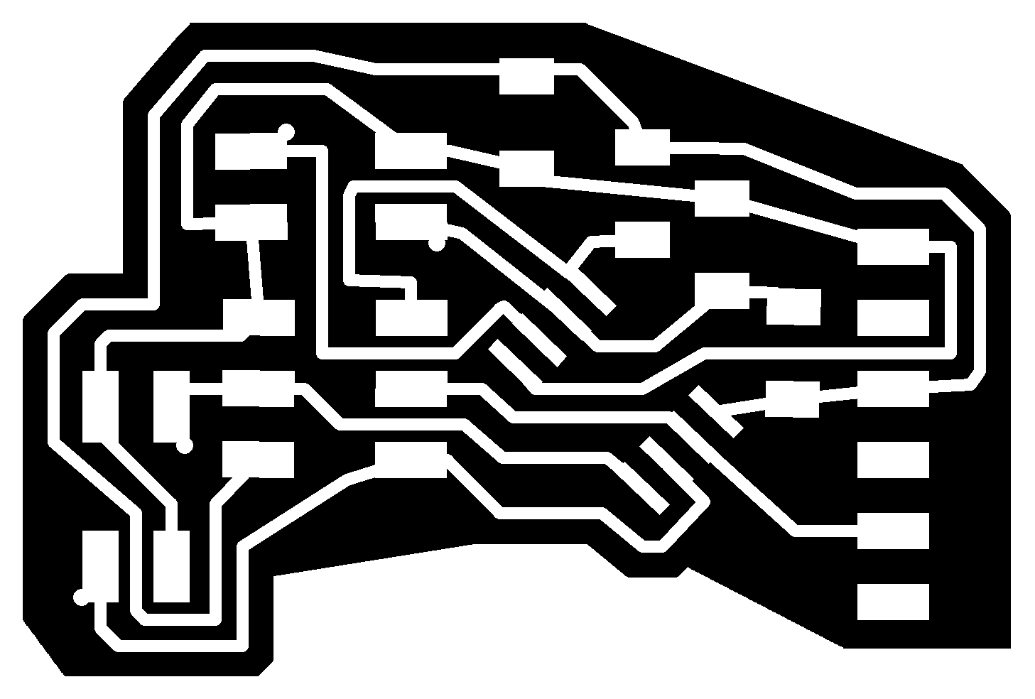
The whole process took me quite a lot of time. It was really difficult to imagine which was the best position to place the components initially to reduce the paths and do not have routes that cross each other. I could not manage to create a network without crossing so I had to use 1 0Ohm Resistor to overcome one line cross. Actually, I also realized that having the MISO and MOSI pins of the SPI available in the pin header for external connections (I called it GPIOT) was really problematic, so I finally decided to remove those connections. The new pin header GPIOT had only 4 connections: TXD, RXD, GPIO1, and GPIO2. The current version of the board is shwon in Figure 11.
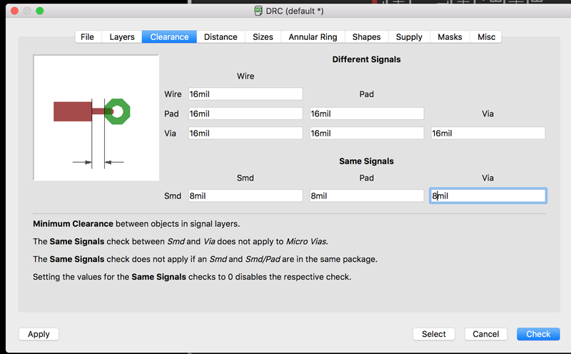
Once the board was ready I firs inspected visually, using the Show object button, that all the connections were correct. After that, I run the Design Rule Check to check if the clearances were correct. Before I had to configure those values in the Clearance tab of the DRC(Figure 12). I set all the values to 16mil (the size of the milling bit: 1/64 inches)
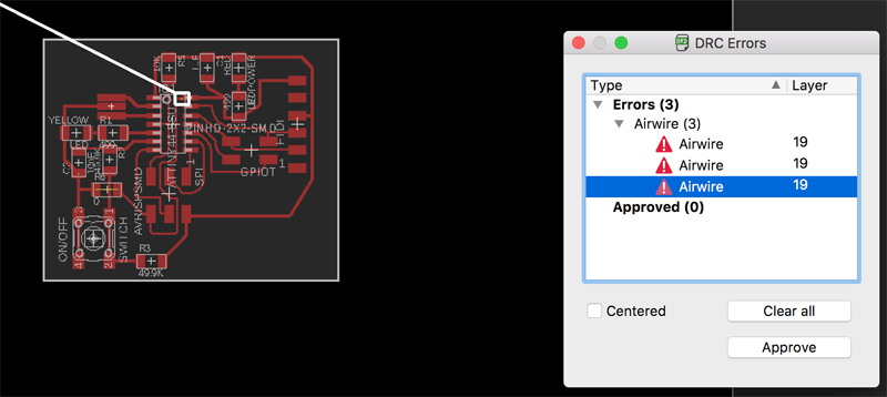
The clearance test return several errors, because some lines were really close one from each other (Figure 13), or very close to the pads. To solve the errors I had to move the lines, change the wire bend in some of them and use a finer position for the grid (0.01 inches) in order to position more accurately the traces.
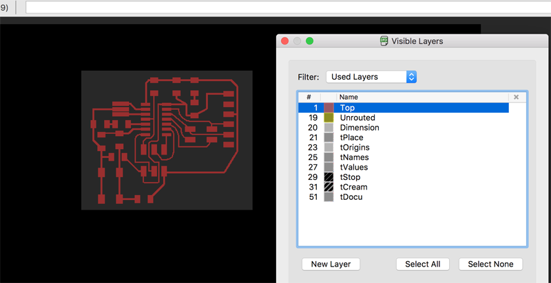
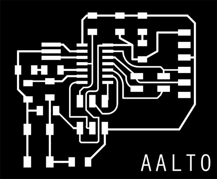
After I managed to remove all clearance errors, I removed all unnecessary layers using the Show/Edit/Hide layers button. I just left the Top layer (the one containing the lines and the Pads). In order to show again a hidden layer you must click on the layer number from the Menu (Figure 14)
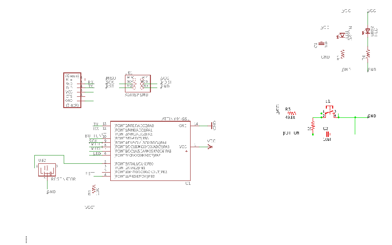
The final result is shown in the following figure:
Next we had to edit a little bit the files before being able to send it to Fabmodules so it creates the .rml. The process is as follows:
- Export the files from Eagle as.png. The resolution I used was 1500dpi. Be sure that you select Monochrome in the Export Menu.
-
To create the cutout and the traces files
- Open the previous generated .png file in GIMP.
- Create a new layer using black as background
- Modify the size of the layer ( Set Layer to Boundary Size ). We want to make bigger the .png file so we take into account the material milled away by the CNC when cutting the board (1/32in=>0.8 mm). So, we extend the height and the width 1.6 mm. Center the layer in the canvas.
- Resize the canvas to the layer's size ( Image>Fit Canvas to Layer )
- Fill the empty area of the bottom layer with black. The visible image is our traces image.
- Fill the traces layer with white. This is the cutout image.
- You can create new layers to add images / text. You can create it as an external file if you want to mill it with other settings.
After creating the .rml file I noticed that some of the traces were so close, that it could only do one offset, instead of 4 (Figure 17). Hence, I decided to go back to Eagle and reduce the width of some of the most problematics line from 0.016 to 0.012. Furthermore, I redo some of the bends to ensure more distance among tracks. The new .rmlfile managed to have at least 2 offsets in all the lines. Final version in Figure 18.

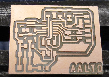
Fabricate the board using the Roland CNC precision milling machine
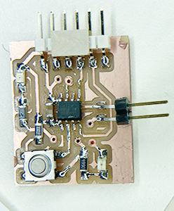
I used the same method as in Week 4 assignment . I had some problems with the board, since it look like that the FSR1 was a little bit bent. Hence, I had to mill it twice, the second time with a depth of 0.25 instead of 0.15 that is the default one that we use for our machine setup. The final board is shown in the following figure
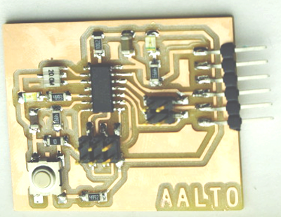
The stuffing process took some time. I still need some practice with surface mounted soldering. However, although it is not a piece of art, I managed to create a working board.
I used the ULP command in EAGLE to export BOD
2021 Fabacademy and moving to Kicad and new Hello board
One of the advantages of being a continuing Fabacademy student is being able learn new and effective trends. With the help of the Videos my instructor Krisjanis Rijnieks developped on how to get started with kicad, I was able to cut the learning curve of this amazing open source circuit designing software. Kris has also developed the fab inventory component library which make designing much more fun.
Taking Kicad as my new tool I moved to complete this weeks assignment by taking the challege of modifing a double sided version of the Hello-ATtiny412_Board from Neil and programming it with the new uopdi programmer I made 2 weeks ago
Individual Assignment: PCB Design Project - ATtiny 412 Double-Sided Board

Materials
| # | Digi-Key Part No. | Name | Value * Pieces | KiCad Footprint(Package) |
|---|---|---|---|---|
| 1 | ATtiny 412-SSFRCT-ND | ATtiny 412 w/ Single-pin UPDI ( Datasheet ) | tinyAVR™ 1 Microcontroller IC 8-Bit 20MHz 4KB FLASH 8-SOIC * 1 | Package_SO: SOIC-8_3.9x4.9mm_P1.27mm |
| 2 | B3SN-3112P | B3SN Tactile Switch, SMD | * 1 | self-designed footprint: TACTILE_SW_B3S |
| 3 |
|
LED 1206 SMD |
|
LED_SMD: LED_1206_3216Metric_Pad1.42x1.75mm_HandSolder |
| 4 |
|
RES SMD 1% 1/4W 1206 |
|
Resistor_SMD: R_1206_3216Metric_Pad1.42x1.75mm_HandSolder |
| 5 | 445-1423-1-ND | CAP CER 1UF 50V X7R 1206 | 1 uF * 1 | Capacitor_SMD: C_1206_3216Metric_Pad1.42x1.75mm_HandSolder |
| 6 | 445-1423-1-ND | Male 1 Row Horizontal SMD Header 2.54MM |
|
self-designed footprint:
|
Design Tool: KiCad EDA
KiCad EDA is a cross platform and open source electronics design automation suite with lots of predefined symbol and footprint libraries provided by industrial companies such as Digi-Key and Teensy . I used it to design my PCB by redrawing the original hello.t412.echo board and adding two extra LEDS (a power LED and a programmable LED) as well as a push-button.
Original hello.t412.echo Board

My Board

Schematic Design

I added the following components and a current limiting resistor between the I/O pin of the ATtiny 412 chip or Vcc (input power) and the component added:
- Power LED
- Programmable LED
- Push-Button
Current-Limiting Resistor for LED
Ohm's law states that the current through a conductor between two points is directly proportional to the voltage across the two points. Introducing the constant of proportionality, the resistance,[one arrives at the usual mathematical equation that describes this relationship: R=V/I,
From the Data sheet of the LED we Know that the typical Forward Voltage is 2.4V and the forward current is 20mA. So Our resistor of choice Should hepe us drop 3V from the 5V Vcc supplied to the Board and saves our led from Burning out.


As can be seen from the calculation the Min required resistor is 130 Ohms but since they don't make that the next prefered one is 150Ohms. Ans in our lab the closest we have to 150Ohms is the 499Ohms and Hence that will be used.

ATtiny 412 Pinouts
In order to program the board, one need to understand the function of each pin of the ATtiny 412 chip . Since ATtiny 412 has an Unified Program Debug Interface (UPDI) pin which is PA0 pin, it is easier to program it with a 1x2 male pin header (J1: Conn_01x02_Male) using the programmer board we milled and soldered two weeks ago.
The other 1x6 male pin header (J2: Conn_01x06_Male) is connected to a FTDI cable or FTDI programmer board to power on and read data from the ATtiny 412 board by communicating through RX (PA1) and TX (PA2) pins.

For the other three remaining port pins, I used two of
them as IO pins to control the programmable LED (PA3)
and the push-button (PA6) respectively. Since I am not
going to use PA7 and the other two pins of the FTDI
male connector, I placed a no connection flag to it to
make sure it does not work against the electrical rules
while I check the performance by clicking

Besides, it is also a good habit to put a bypass capacitor between Vcc and GND pins (power pins) of the chip.

Annotate Schematic Symbols
In order to specify different components, I then opend
the Annotate Schematic dialogue by clicking


Assign Footprint
Before layouting the printed circuit board, I need to
assign which footprint belongs to which symbol
(component) in the Assign Footprint dialogue by
clicking


The name of each correspondent footprint is also arrranged in the material table shown on top of the page.
Generate Netlist
The final step of the schematic design is to generate
the netlist file which will then be imported to the PCB
layout mode. I did this by clicking


Complete Schematic

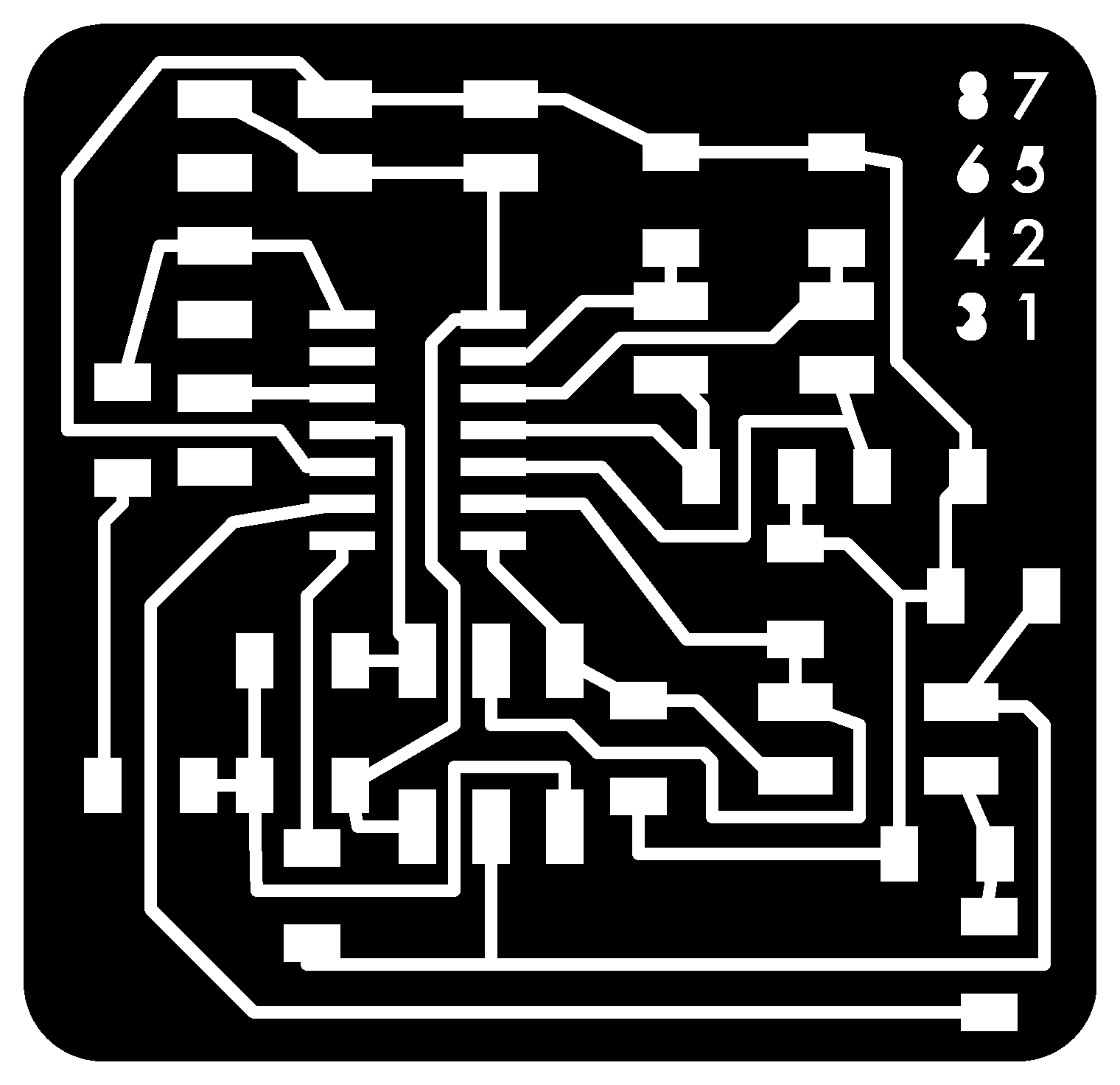
Footprint Layout
After finishing the schematic design, I then switched
to the PCB layout mode via


Import Netlist File
In the PCB mode, I clicked

These are some messy nets which I am going to layout:


Define Trace Clearance, Trace Width & Via Size
Before starting to connecting components with traces, I
clicked Board setup button

-
Clearance
- For normal traces which can be milled with 0.4mm bits: 0.4mm
- For tiny traces (e.g., smaller SMD chips) which can only be milled with 0.3mm bits: 0.3mm
-
Track Width
- For Default traces: 0.4mm or 0.3mm
- For Power traces (e.g., Vcc and GND): 0.6mm or more
- Via Drill: 0.8mm (depending on the size of copper hollow rivets introduced below)

THT Settings
In order to mill THT components, I need to first adjust
the hole size of certain components in the footprint
library by clicking Open footprint editor button

I double clicked its pin holes to open Pad Properties dialogue, typed the correspondent size (here, 1.5mm for Hole size X) and made sure that the pad size of this hole is big enough for soldering by adjusting Size X and Y.

Separate Layers
After layouting all the components, I started to create
traces between them by using

If there is not enough space for routing tracks, I then
created
vias
which are conductive holes by using


Since there are many pins connect to GND, it is also
useful to create a ground plane on the other side by
switching to B.Cu layer and using


The final step of the PCB layout is to define its
outline for
mods
to generate its interior toolpath. To do that, I first
switched to the Edge.Cuts layer and used


Finally, I added a pink rectangular outline to the Margin layer which is reserved for the drawing of circuit board outline. Any element (graphic, texts…) placed on this layer appears on all the other layers. It also defines the board area for exporting the image for each layer.
Complete PCB View & Final Check
Below I listed some notes according to different layers:
-
Edge.Cuts layer: yellow outline
- every component (including gray texts and green footprints) should be inside this layer.
-
Dwgs.User layer: gray fill
- the size of this layer should be the same as Edge.Cuts layer.
-
Margin layer: pink outline
- make sure there is no gray texts in this layer, otherwise there will be some flipping problems during milling.
- make sure the left and right margins are even by specifically defining the coordinates of two vertical lines along x-axis in Line Segment Properties dialogue.

Export PCB SVG
Before starting milling the board, we need to generate the image files for its front-side traces, back-side traces, drilling and outline. I did this with the following steps and settings:


For the drilling svg, I filtered out the vias from the F.Cu.svg and infilled them with black color in Inkscape :

Fabrication: SRM-20 Milling Machine
The fabrication of the PCB is almost the same as the process of Week 4: Electronics Production except the server module used to generate the cutting toolpath in mods is:
p.s. MDX-40 milling machine uses the follwing same svg mods server module.

mods Toolpath Setting Comparison (MDX-40)
Link to AALTO fablab youtube tutorial using MDX-40 milling machine
- origin: (x, y, z) = (0, 0, 0) mm
- home: (x, y, z) = (0, 0, 5) mm
| tool diameter | cut depth | max depth | offset number | speed | color |
|---|---|---|---|---|---|
| 0.2mm (new) | 0.125mm | 0.125mm | 4 | 20.0mm/s |
|
| 0.4mm | 0.125mm | 0.125mm | 4 | 1.5mm/s |
|
| 0.8mm (Outline) | 0.6mm | 1.8mm | 1 | 2.0mm/s |
|
| 0.73mm (Drill) | 0.6mm | 1.8mm | 1 | 2.0mm/s |
|


Link to the testing with lab equipments: Group assignment
DOWNLOAD FILE
Eagle File -
Eagle File
RX-TX board Trace-
RX-TX board Trace
RX-TX board cutout-
RX-TX board cutout
8 PIN INPUT board Trace-
Trace
8 PIN INPUT board cutout-
cutout
8 STRIPE CAPACITIVE SENSOR -
Trace
cutout