
Overview
This week we only had to mill a board, but I wanted to understand the process of designing the board already. I had no experience with this before, so I started from scratch. I decided to use Eagle because it was recommended by the other students and instructors. I am able to work with it now, but halfway through I got the tip to use KiCad the next time, as it is easier for beginners, open-source and also powerful. Especially the standard library of parts is much easier to find what you need.
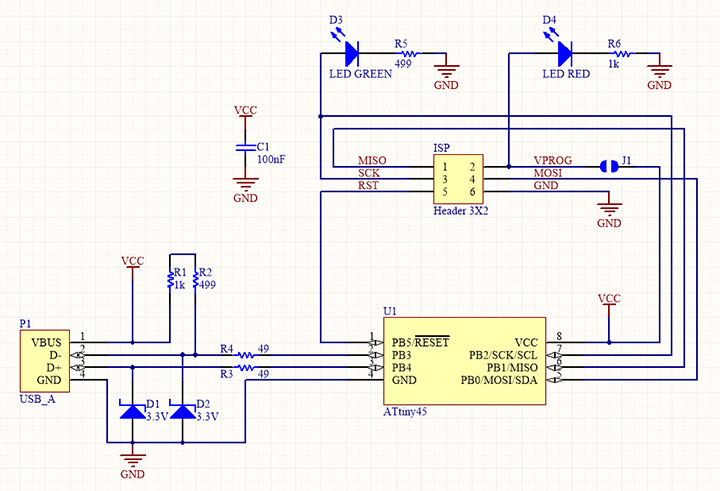
I decided to just redraw the FabTinyISP from Brian to get started with Eagle. Sparkfun has really good tutorials for Eagle to get to know what you need to do, as Eagle is not really intuitive. The basic workflow of eagle is: First you create a schematic (circuit diagram), which is just the description of all the electronic components you want to use and how they are connected. Afterwards, in a second step, you create a board layout from these parts. But now you already have all the parts available from the schematic do and "only" need to arrange them on the PCB.
Designing the schematic
I started with opening the image of the schematic and the ISP board as a reference to work along. After opening Eagle, you need to create a new project and then add a schematic to this new project. Before you start you should download the Eagle libraries for usb and fabacademy and put them into your eagle library folder (This can be found in Options->Directories in the main eagle windows). I followed this tutorial to create the schematics and will explain the most important parts, changed things and show some new screenshots in this chapter.
The first part of designing the schematic was for me adding all the parts to the board and afterwards wiring all them together. Of course, you can mix them as you like.
Adding parts
When you clock on the add part button you can add parts from a huge list. Also, you can click on Open Library Manager in this window to see all available libraries and load more (like the fabacademy library for example). For every part you get the schematic and board symbol shown to decide which of the versions of the part you want.

Adding parts and library manager.
After Clicking on Ok you can click anywhere to place the part there. Or repeat the process to add other parts. One big drawback of eagle is the huge library of parts, which have cryptic names and you never know which to use. My tip: The fabacademy library already has the most needed parts predefined and the rest can be found by searching for it - the search field uses regex, so make sure to search for *led* if you want to find all led's. Another hint is the Sparkfun library, which is clear categorized and has a lot of parts.
To move parts around the workspace you need to select the move tool on the left side, left click on the cross of the object you want to move and then click to the position you want to move it. Rotating, mirroring and deleting are working the same.

Eagle after adding all the parts.
Connecting the parts
To connect parts together you can click on the Net tool. Then you click on the connector of a part, and then onto another. They get connected by a wire. You can also click on a wire, so the connector gets connected to this wire. This is indicated by a green dot on the wire.

Eagle after connecting the parts.
Adding details
You can also add details like the values of the resistors and capacitors to your schematic. It is useful when you search for the parts to have all the information you need available in your design. Therefore you click on the Info tool and slect the part which information you want to change.

The finished schematic in eagle.
Designing the board
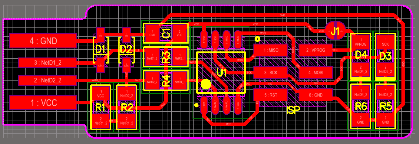
After the schematic is finished the next step is to arrange all parts on the board. Here I mainly followed this tutorial. First, in the open schematics you need to click on the button Generate/Switch to board, which is shown in blue in the last picture. Then you just get all your parts put into the board design tool:

After switching to the board view.
Moving the parts
First, the parts need to be moved and rotated to the positions they should be at, this is done in the same way as in the schematics view. Here the ISP board template is very helpful.

The arranged components.
Routing the connections
Now the connections need to be routed. Therefore you can also mostly do the same as in the template, otherwise this step requires a lot of moving parts around. Similar to the connection in the schematics view, now you select the Route tool and click on one connector for one component. Now all the pads you need to connect this pad to get highlighted, so you easily see where you need to connect it. One thing that is useful here is when you click on empty area while routing, then the route up to this point will be fixed. That is helpful especially when adding complex lines. You can also choose the Width of the routing, so the line won't be too small to cut or too big to hit other lines in small parts.

The routed PCB lines.
Creating the outline
To create an outline where the board will be cut off you can use the line tool. But before drawing you need to change the layer to the Dimension layer.

The finished eagle board.
Checking design rules
Design rules are rules that an check if your board can be manufactured and to check for errors. After clicking on the design rules button you get a window where the design rules are specified. If you already know which i.e. clearance you need for your machine and soldering skills you can change the value there, otherwise you can just leave it on default and it will tell you if you did some mistakes.

The design rule check window.
For me, the program told me that there is an error because I still have an airwire on my board. When clicking on it it also shows where it is. Airwire means I forgot to route one connection. This step is pretty important as I actually didn't do it the first time, forgot to route one connection and ended up with fixing my PCB with a wire. The Restrict errors are around the USB connector, which looked fine, so I just ignored them.

The design rule check results.
Milling
Our fablab has an excellent tutorial on how to use our PCB mill (LPKF S62). As there are several steps you need to take the tutorial is comprehensive, but it is best to work through it step by step when you want to mill a PCB. With this tutorial, my prepared eagle files and somebody watching me I was able to use the mill without any problems on the first try. I will outline the important steps, details can be found in the tutorial.

The PCB mill.

Putting a board in the mill.
The first step is to copy the prepared eagle files to the pc next to the PCB mill. Then you start BoardMaster on the PC. Then you start eagle, export the created files using the CAM processor. These files you can open in CircuitCam for further editing. There you generate the outline, mark places where the copper is to be removed completely and export it to the BoardMaster milling software.
An important hint here: As you are working with different programs make sure to load the correct file each time! I loaded the board of another student, which looks similar enough on the first look and milled it the first time, because the standard opening directory is still set to the last directory. So be sure to get that right.

The BoardMaster software
In the program, you can see a camera image to place the milling head precisely. On the left, you can see the head position, working area and the PCB.

The finished board after milling, the ATTiny already placed on it
Soldering
Bill of material:
-ATtiny45 (SMD)
-2x3 pin header (SMD)
-100nF Capacitor (SMD)
-2x 47Ω resistor (SMD)
-1x 470Ω resistor (SMD)
-1x 560Ω resistor (SMD)
-2x 1kΩ resistor (SMD)
-2x Diode (SMD, 3.3V)
-LED (SMD, green)
-LED (SMD, red)
I already have a bit of experience in soldering and our local instructor also gave us an introduction to soldering which still helped me to remember what is important. If you are new to soldering, you can have a look at the soldering is easy comic. Page 5 has the hint that helped me to remember to preheat, apply the solder to the contact point and then wait again. The rest is very basic stuff.
I started by collecting all the parts and put them on tape, because otherwise the small smd parts are easily lost. I also put numbers on the tape to remember which of the resistors was R1 and which R6.

All parts on crepe tape
When picking the parts I realized that we don't have exactly 500Ω and 50Ω resistors, so I took 47Ω, 470Ω and a 560Ω resistor next to the led. This is not updated in the schematic, but it is updated in the bill of materials.

Started soldering the attiny, as this is the most complicated part. First i put solder on one of the pads, then put the attiny on top of the solder with a tweezer. Then I heated the solder again to fix the attiny in position.

I next soldered all the legs of the attiny into place, then the two diodes. There I hold the diode in place with a tweezer while heating the solder again.

I wanted to test how to work with solder paste instead of regular solder (wire). So I used a needle to put some solder paste on the pads for the next part. This was really fiddly. Placeing the part then was easy, it also sticked to the solder paste.

The I heated up the solder paste, which fixed the resistor. This step was no different from the normal solder. It is too much work to apply solder paste by hand so I switched back to solder wire for the rest of the board.

Putting in the next resistor

To speed up the process I put solder on all the pads were left.

I soldered the parts onto the board and also connected the jumper with solder. That was when I realized i forgot to route one connection between the led and resistor on the right side. This I fixed with a wire, which can be seen in the next image.

I added the wire, the last led and also the header. The header went in last, because it was the biggest part and would be in the way for everything else. For the header I started with one pin to hold it in position, and then did the rest.
As the last step I added solder to the USB pins, so that I could use the board in a regular usb jack.

The finished board
You can clearly see that it is not really nice soldered, the parts are skewed, there is too much solder on some parts, the solder doesn't look very good if you look closely. But I still decided to test the board, as it looks solid enough. But I was surprised that you can solder all these really small parts by hand.
Debugging
After soldering I tested all the connections with a multimeter, so that no pins or traces are connected that shouldn't be connected. This is especially important (for the USB pins), because if there is a short you can damage your laptop! So be sure to double check.
To check for connection on the UNI-TREND UT61A you need to set the big rotary switch to the second option. Then press the blue button until in the display the sound symbol is shown. Test it by holding the two probes together, the multimeter should beep.

The multimeter to test connections
Fortunately for me I had no shorts and also no problems later which needed debugging.
Programming
I am using Windows and wanted to use the Windows Subsystem for Linux to program the ISP, because I thought it would be easier this way. Programming the ISP works fine, but using the ISP for programming is not possible, because the WSL only supports USB devices that are either Serial Ports or USB media drives. So the process shown here is based on Brians tutorial and especially the windows part of it. I will explain this setup in the electronics design week to program another board.
First install the drivers for your programmer, in our case we use a mySmartUSB MK2, you can get the driver here. You need to connect the programmer with your FabTinyISP. A pinout diagram for the programmer you can find in the linked manual on page 5. For the FabTinyISP you can find it in the eagle files. Then you can connect the programmer with your laptop. The red LED on the FabTinyISP should light up then.

The red LED lit up
Now we come to the setup with WSL, follow the tutorial from microsoft on how to install WSL, if you haven't already. Then first run sudo apt update and sudo apt upgrade to update the packages. Then install the necessary packages with the command
sudo apt install -y avrdude gcc-avr avr-libc make unzipDownload the firmware with
wget http://fab.cba.mit.edu/classes/863.16/doc/projects/ftsmin/fts_firmware_bdm_v1.zipand unpack it with unzip fts_firmware_bdm_v1.zip. Go to this directory cd fts_firmware_bdm_v1.
You need to change some stuff in the Makefile, as we are not using the usbtiny ISP. Change
PROGRAMMER ?= usbtiny to
PROGRAMMER ?= avr910.
To connect your programmer (it needs to use serial connection) to the WSL, you need to find the COM port number of your programmer in the device manager.

The programmer in the device manager
Then you can connect it to the WSL with the command chmod 666 /dev/ttyS10. Where 10 is the port number you have seen in the device manager. You also need to replace all the occurences of -P usb to -P /dev/ttyUSB10 in the Makefile. To compile the software run make. To erase the attiny and program it with the firmware run make fuses. This command configures the fuses of the attiny to get the clock from the PLL, so that it can be used as a USB device. During this operation the green led should flash a few times.

Both LED's are flashing
To test if this has worked now disconnect your programmer from the FabTinyISP and plug it in the usb connector. In the device manager you should see a device that is not recognized correctly, like seen below. To install the driver download zadig, which can install the generic libusb driver. Select the correct device, change the driver to libusb-win32 and click on install driver.

The ISP gets correctly recognized by windows
After the driver installation the exclamation mark from the FabTinyISP should be disappeared like shown below.

The ISP gets correctly recognized by windows
If the last step worked and the isp gets recognized as a USB device you can configure the fuses so that the reset pin will be used as an input/output pin. But then you won't be able to change the firmware on the programmer again, so make sure it is a working USB device. Then run make rstdisbl. If you want to program circuits which draw a lot of power you should disconnect the solder jumper and power the circuit externally.
Files
Here you can download the files created during this week:
The Eagle Files for the ISP