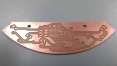
Dual sided circuitry
Peaks, plateaus and pitfalls of dual sided circuitry.

Step 1: Read guides and tutorials, and test specs.
There is surprisingly little material available on making two sided circuits on the modela milling machine. There are a few things to consider: Holes, rivets, alignment, milling bits and how to actually draw the circuit in Eagle.
One of the most helpful tools to get started is the Fab tutorial on PCM rivets. It details the process for rivetting a circuit boards. The rivets we use for circuits are either 1 or 0.6mm in internal diameter. If you need to pass a wire through the hole, you probably need the bigger diameter, but for my project, the 0.6mm rivets work just fine. I decided to mill the test from the tutorial to see how it works on our machine. My conclusion was that a 0.69mm hole is the best size for our machine.
I also did a second test, to be certain of the drill diameter for Eagle.
Tutorial on PCB rivets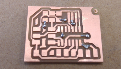
Step 2: Test the design parameters and match them to the specs.
Now that I had the best hole size, I felt pretty ready. I even drew, milled and soldered a test hello board, then programmed it. There were a few issues. Because I placed my vias haphazardly during the process, some of them weren't properly spaced, and I had to cut some copper away to remove a short from the board. Additionally, while the rivets worked, I had to do a lot of post-processing to my image after the eagle work was complete in order for the holes to work on the Modela.
Therefore, the proper "step 2" Is to draw up your own hole test in Eagle, where you find the correct diameter and drill settings for your vias before you draw your circuit. The goal is to draw them so that they can be exported directly, without any further need for processing.
Step 3: Mill your test
One of the issues with our modela during this process was that it looses the z axis aligment in between cuts. Normally, this is not an issue since we always send it to view mode, switch out the milling bits from 1/64" to 1/32" and back, depending on the job, but when making holes, you use the same milling bit for the holes and the outline, meaning that I did not see a need to re-zero the z-axis, resulting in a spectacularly broken milling bit.
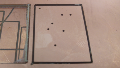
Another issue can be that if your holes are drawn too small, the fabmodules won't be able to see them or see any way to mill them. They need to be "just right", so that it will drill them in the correct size. The test is not two-sided, so aligment is not an issue yet. We'll discuss alignment later on. For me, the best drill size setting is 37 mil, with the radius set to "auto".
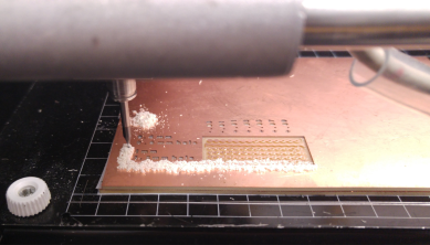
Finally, the milling bit can get gummed up with the dust from the plastic and the copper that is being milled. I had to clear the flutes three times on average per board. If your milling bit just sort of taps down and makes a shiny little spot, it's a sign that your flutes are clogged and you need to stop the process, remove the bit and clean it, then replace it before continuing.
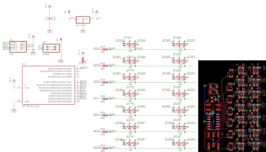
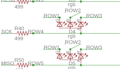
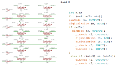
Step 4: Draw your circuit
Now that you have your preferred hole size and the correct settings for Eagle, draw up your circuit board. In order to activate the back layer of copper, go to the DRC menu and select layers. In the dialog box write (1*16) This designates the top layer as layer 1, the bottom layer as layer 16 (which is the standard layer for the bottom) and says that they have an insulating layer in between.
When routing your board, clicking the middle mouse button will allow you to go between layers, each middle mouse click will allow you to place a via, then you can continue the route on the other side. It takes a little while to get used to but is really quite fast once you get the hang of it.
Step 5: Milling and aligning
Most of the guides call for alignment brackets, but the best practice I've found for milling two-sided boards on the Roland mill we have is:
Be careful to remove any dust that may have settled on either layer, remove any old tape and apply fresh tape for the second cut. You need the circuit board to be firmly fixed to the sacrificial layer before doing the front trace. On our mill, the board needs to be approx half a mm away from the edges on all sides of the hole.
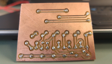
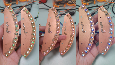
Step 6: Riveting
If you followed the steps above you already riveted your tests, but for form's sake, I wanted to mention this step. Take your rivet, for my board, I need the 0.6mm rivets. Place it in its hole, then with a fine point, hammer it so it folds out, then with your hammer, whack the board, so the rivet becomes flat and beautiful. Whack it an extra time if you are frustrated because this took so long. Do it now, before you solder anything on it that can't handle a good whack. Repeat for every single hole on the board. All of them. Then solder your rivets to ensure good conductivity between the traces and the vias. Solder on both front and back. This is your life now.
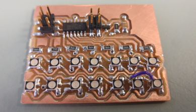
Step 7: Soldering
It is helpful to cut a frame for your circuit board, so that once you have soldered components on one side, you can flip the board over and solder the back. If you only have components on the front, like I do in my example, solder as normal.
Later, I created more dual-sided circuit boards, and I used a clamp to hold the board steady and off the table while I soldered it.
Step 8: Troubleshooting
I was in a hurry and soldered 6 resistors to the wrong pins before realizing. I then rushed the removal, ripping some of the ends off before resoldering the same resistors. This was bad, because that of course means that the resistors do not function any more.
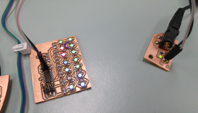
Once I resoldered the resistors, the board funtioned as well as could be expected. The traces are not all as thick as they should be, because I failed to use the correct drc settings. This means that I needed to connect some points with airwire, and others are still not working properly. Still, this is a functioning prototype of the LED boards I want in my final design, so the effort was worthwhile.