
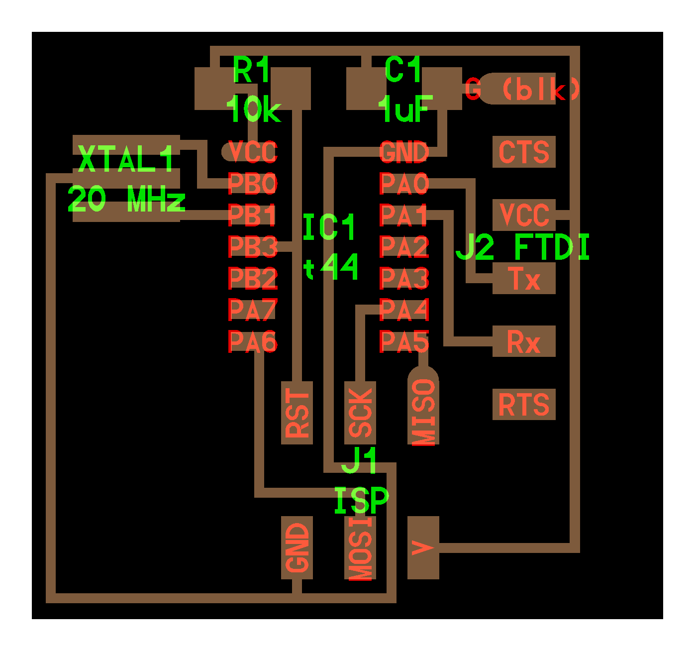
For this design the software Eagle Version 8.6.3, provided by Autodesk, was used. The program KiKad was also tested. It will be commented later in the text.
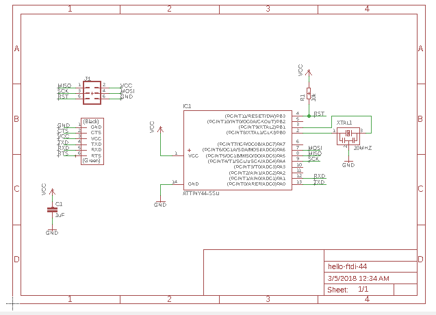
After downloading the fab Lab library, and activating it, we downlad the document hello.fdti.44 schematic. Modifications have been made to this open source file.
Workflow:
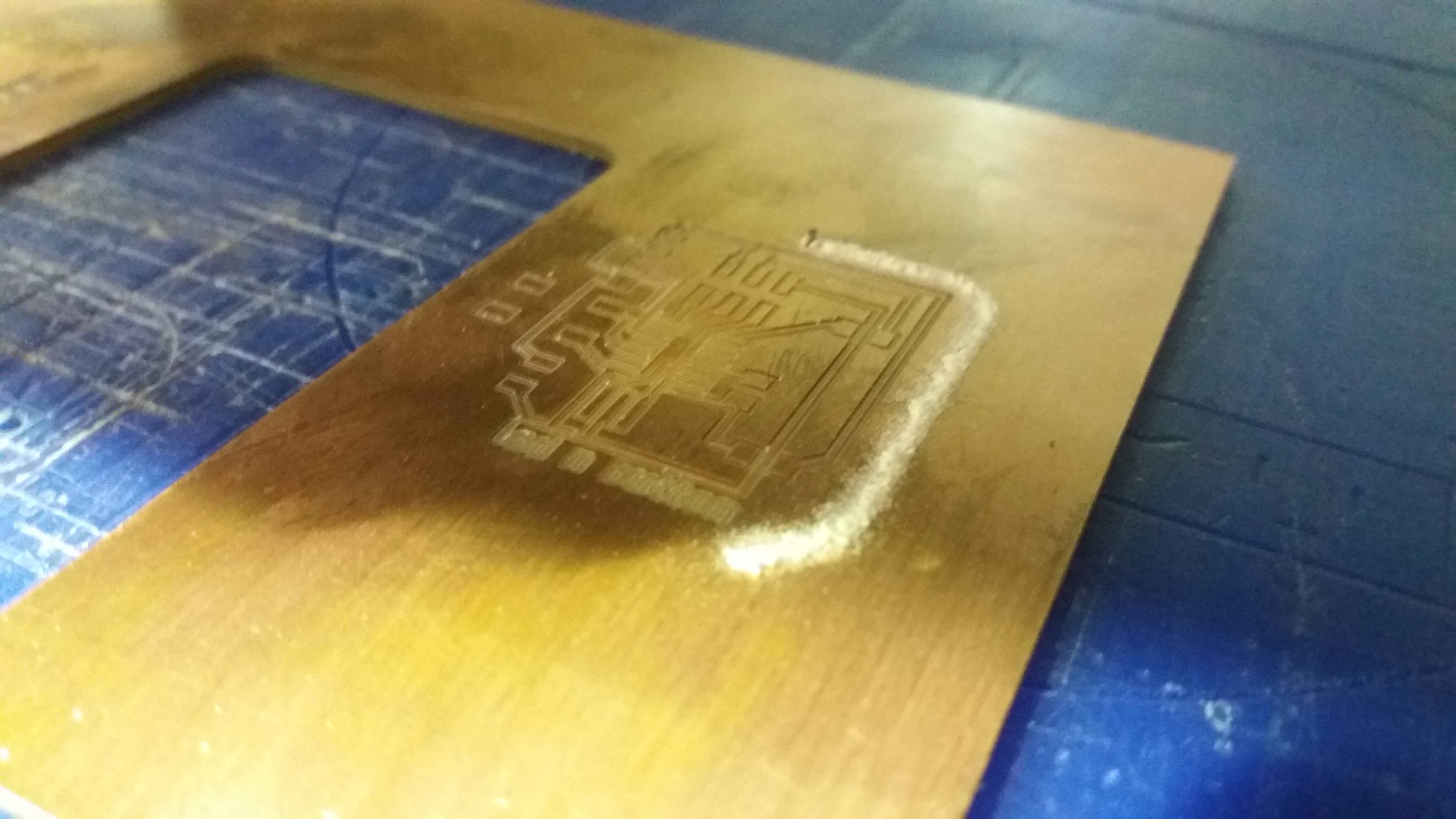
First, we milled this board:
Milling at this point was a mistake, but we can take this opportunity to hack the board.
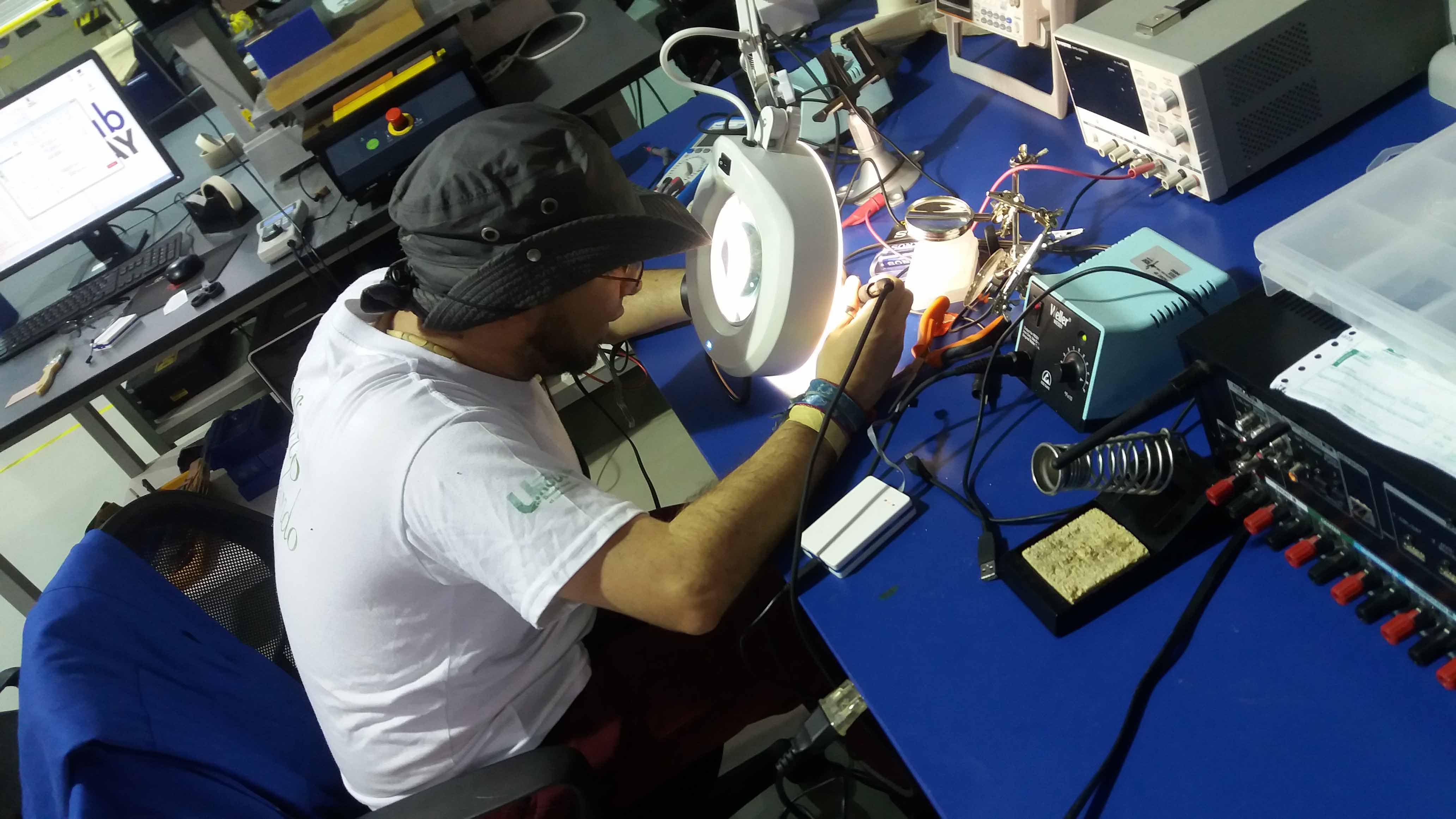
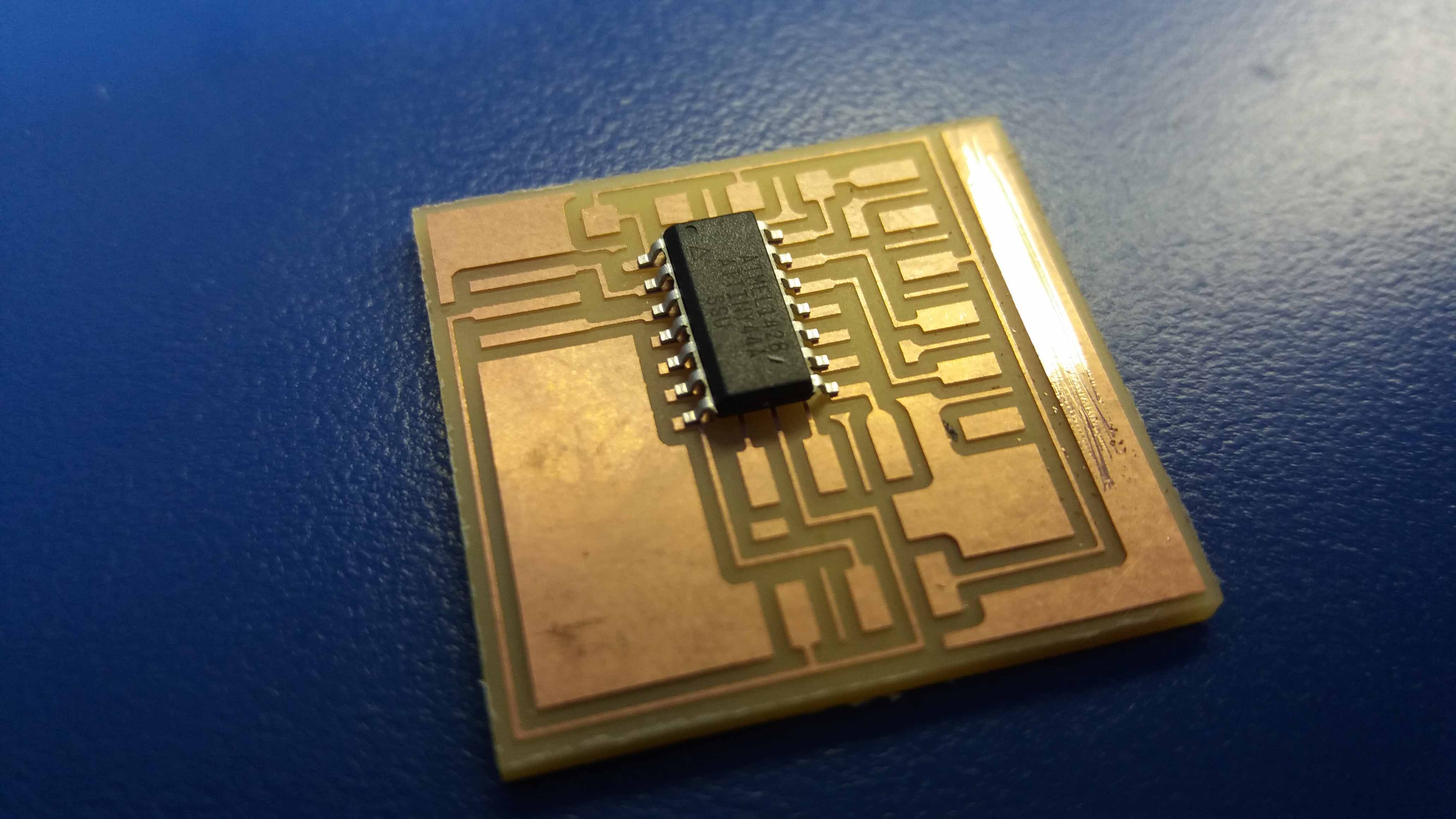
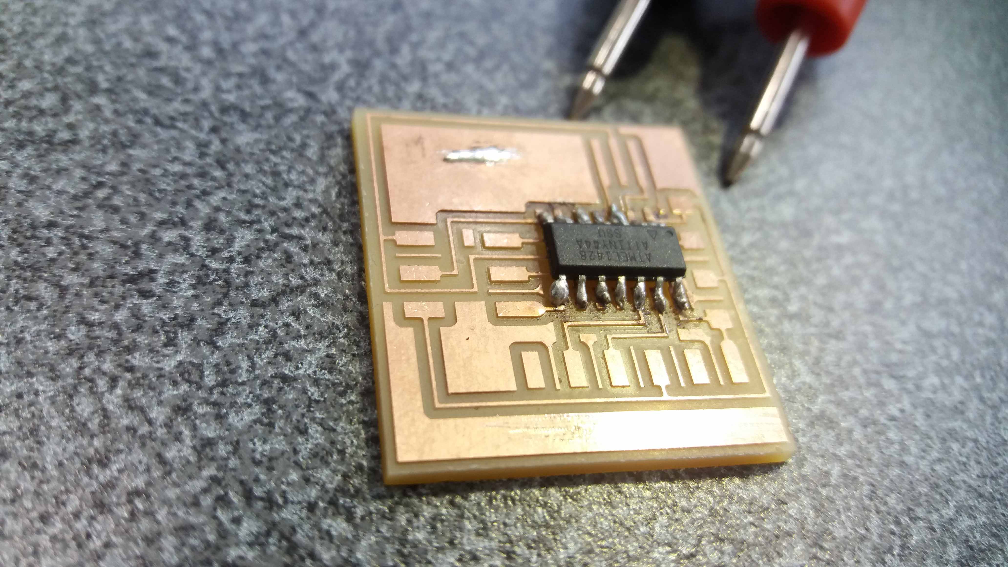
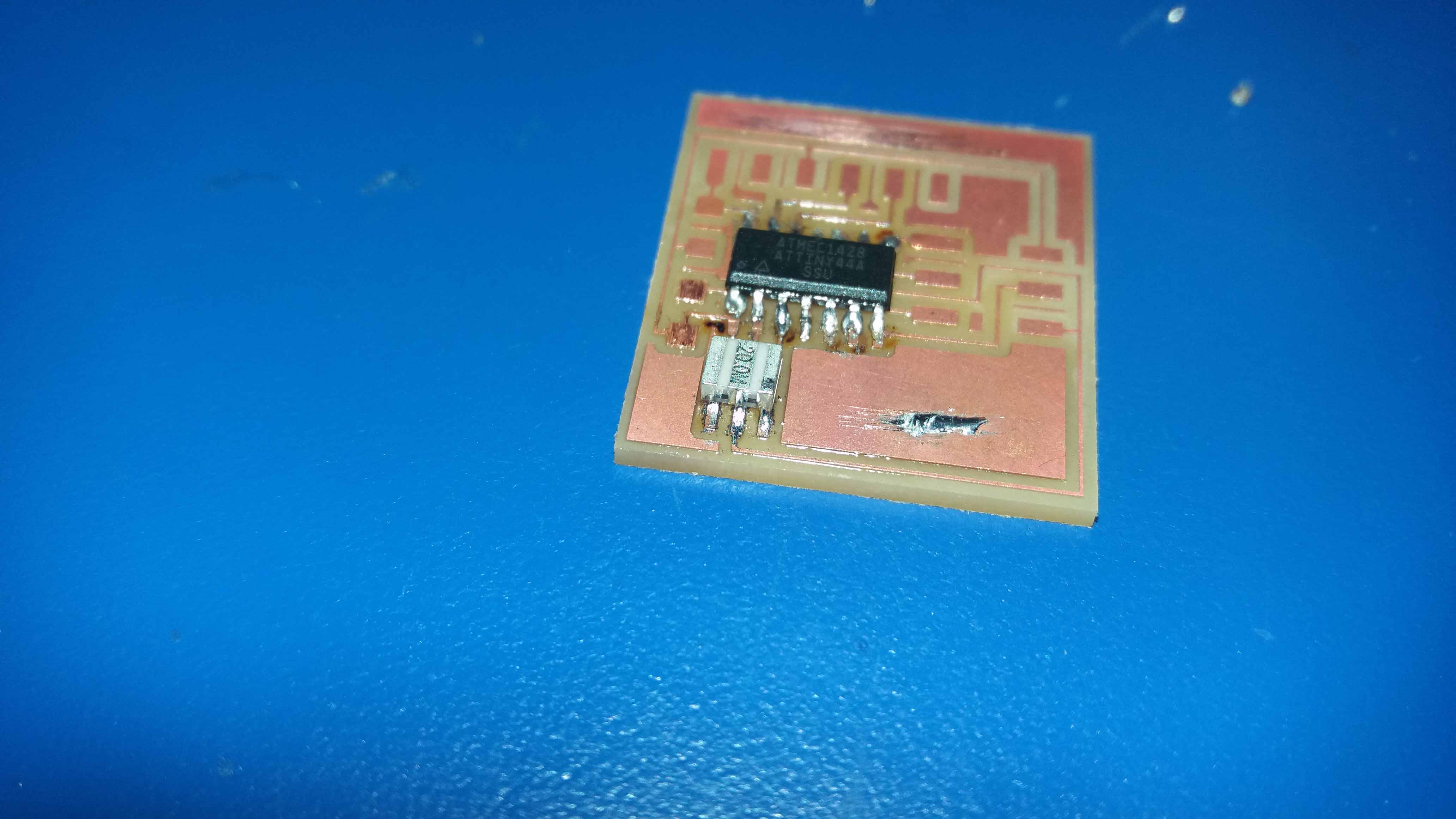
We place the microcontroller chip on the board with the right orientation. Then we soldier the pins, and test the connections with the meter.
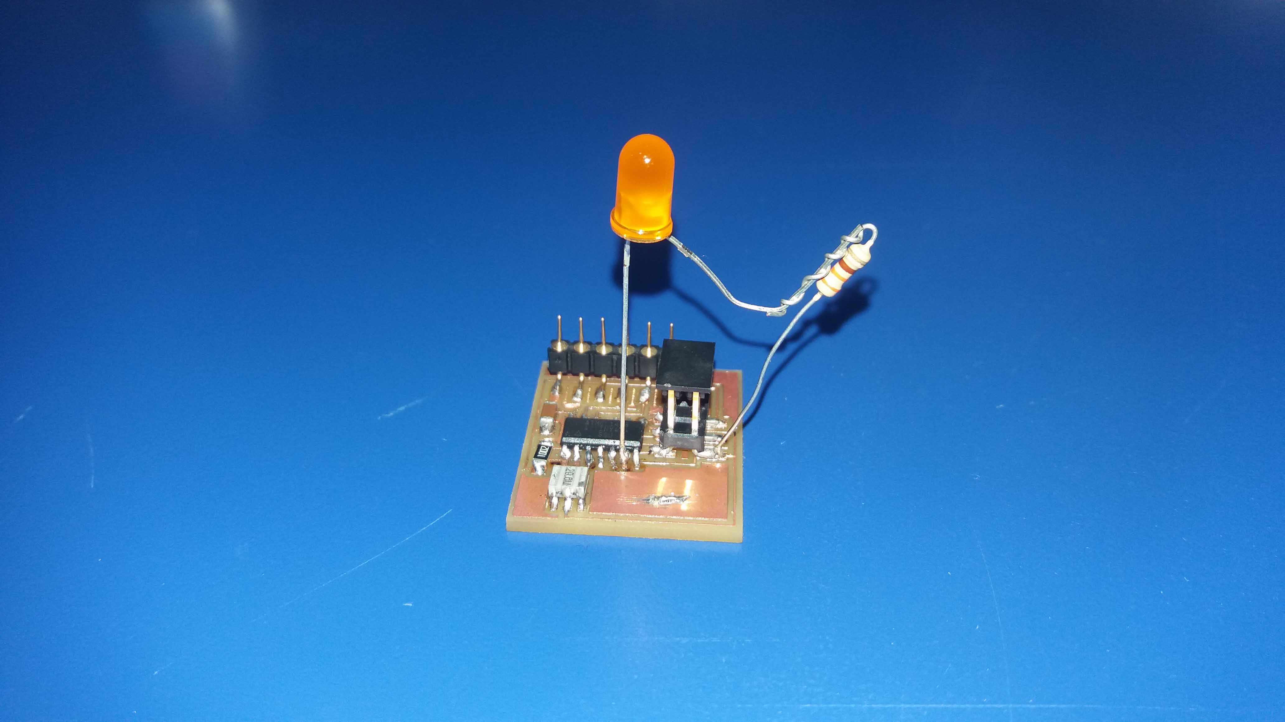
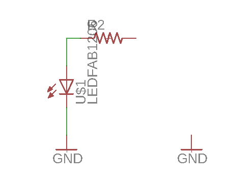
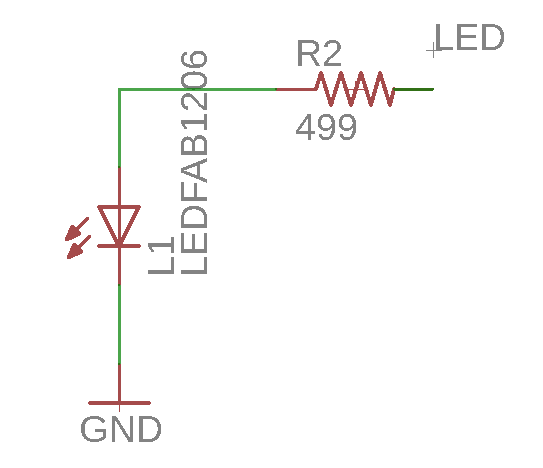
Then we place the crystal and connect a current limiting resistor in series with an LED.
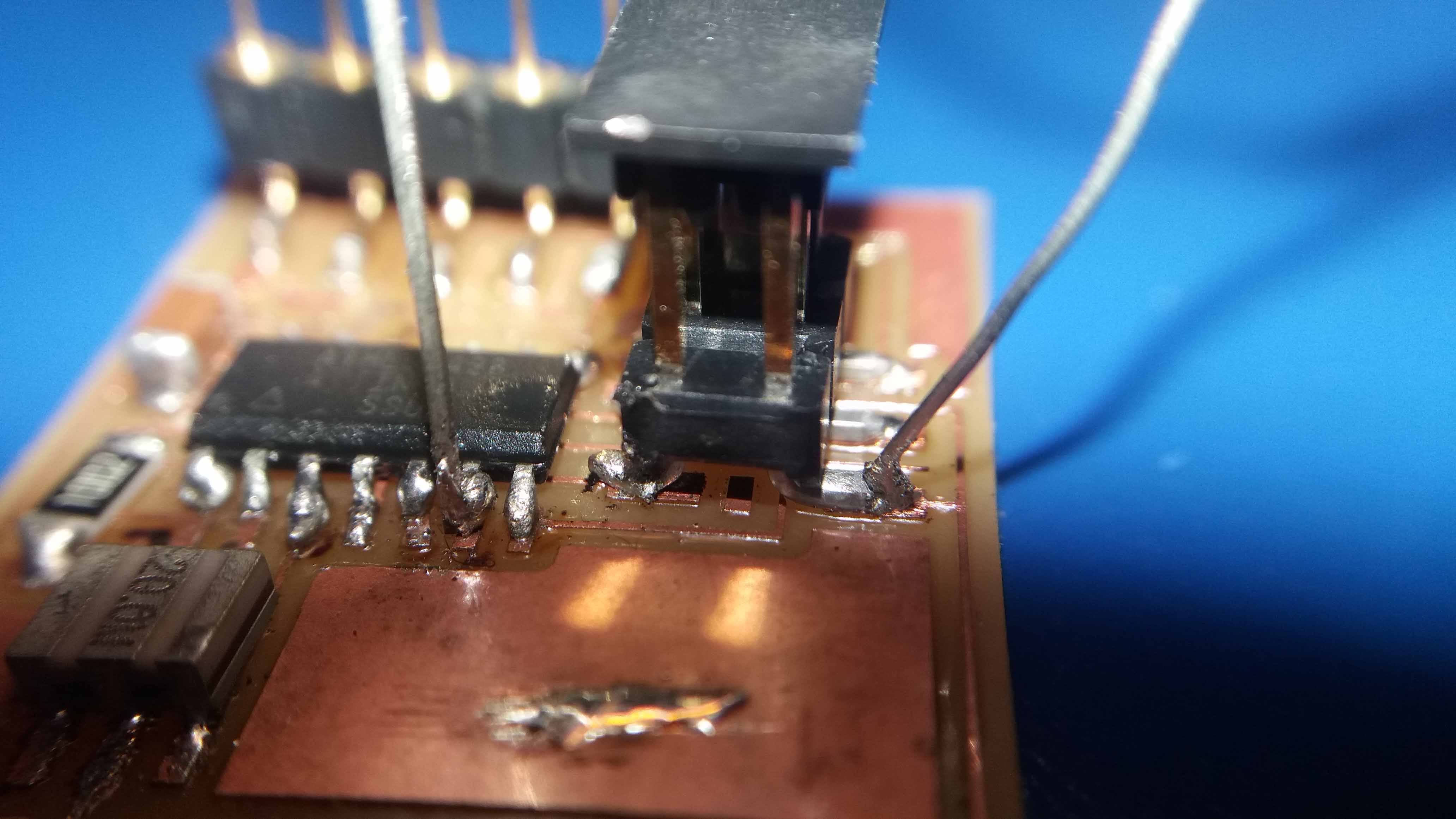
In this close ups we can see the anode (positive terminal) of the led connected to a free pin on the microcontroller. The cathode (negative terminal), is connected to a limiting current resitor to protect it, and then to the grownd on the board. We still have to load a program to it. I will do so when I solve the problems I have with the software/hardware programmers. For testing, I will use the clasic "blink" program.
Assigment update
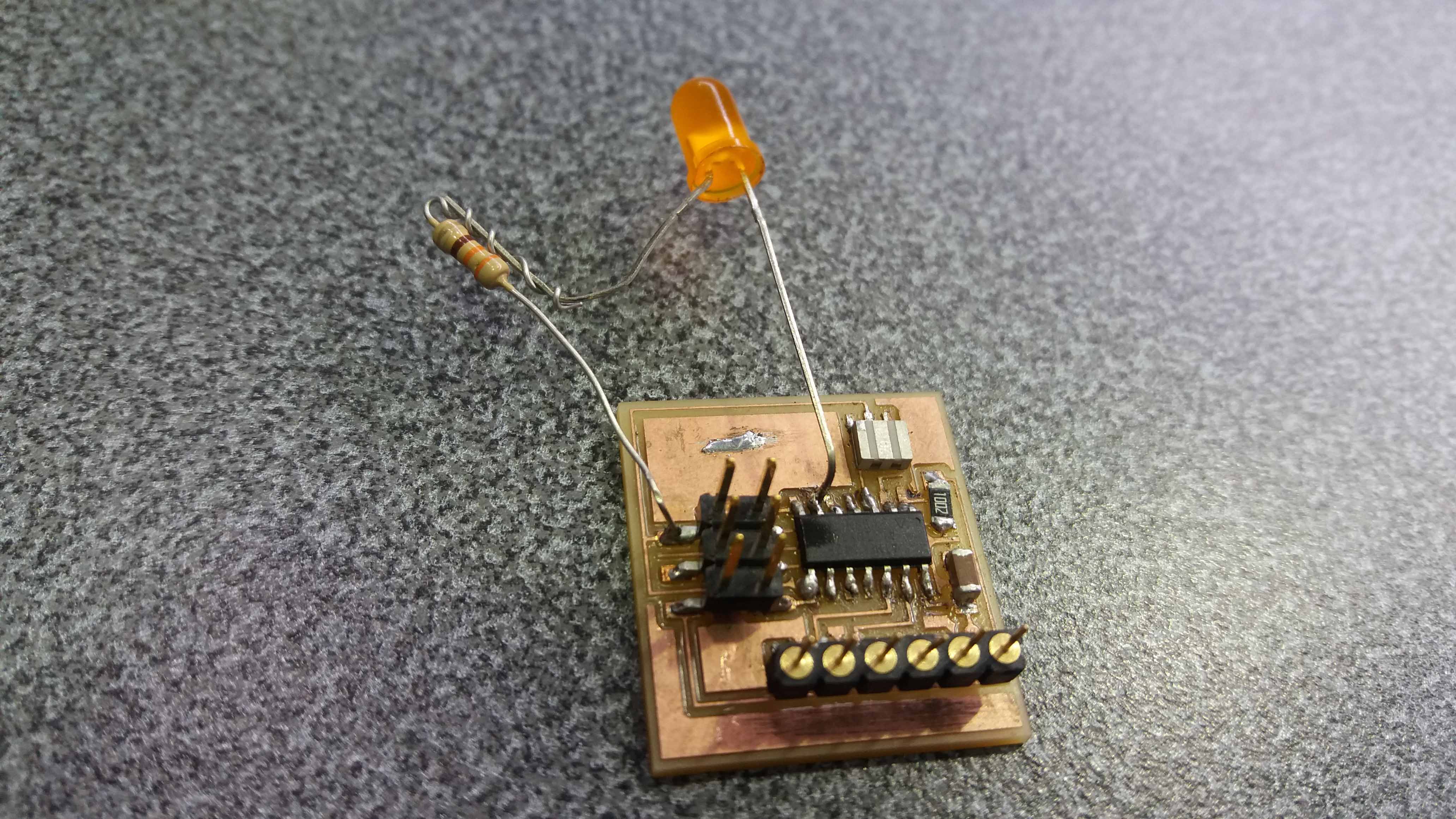
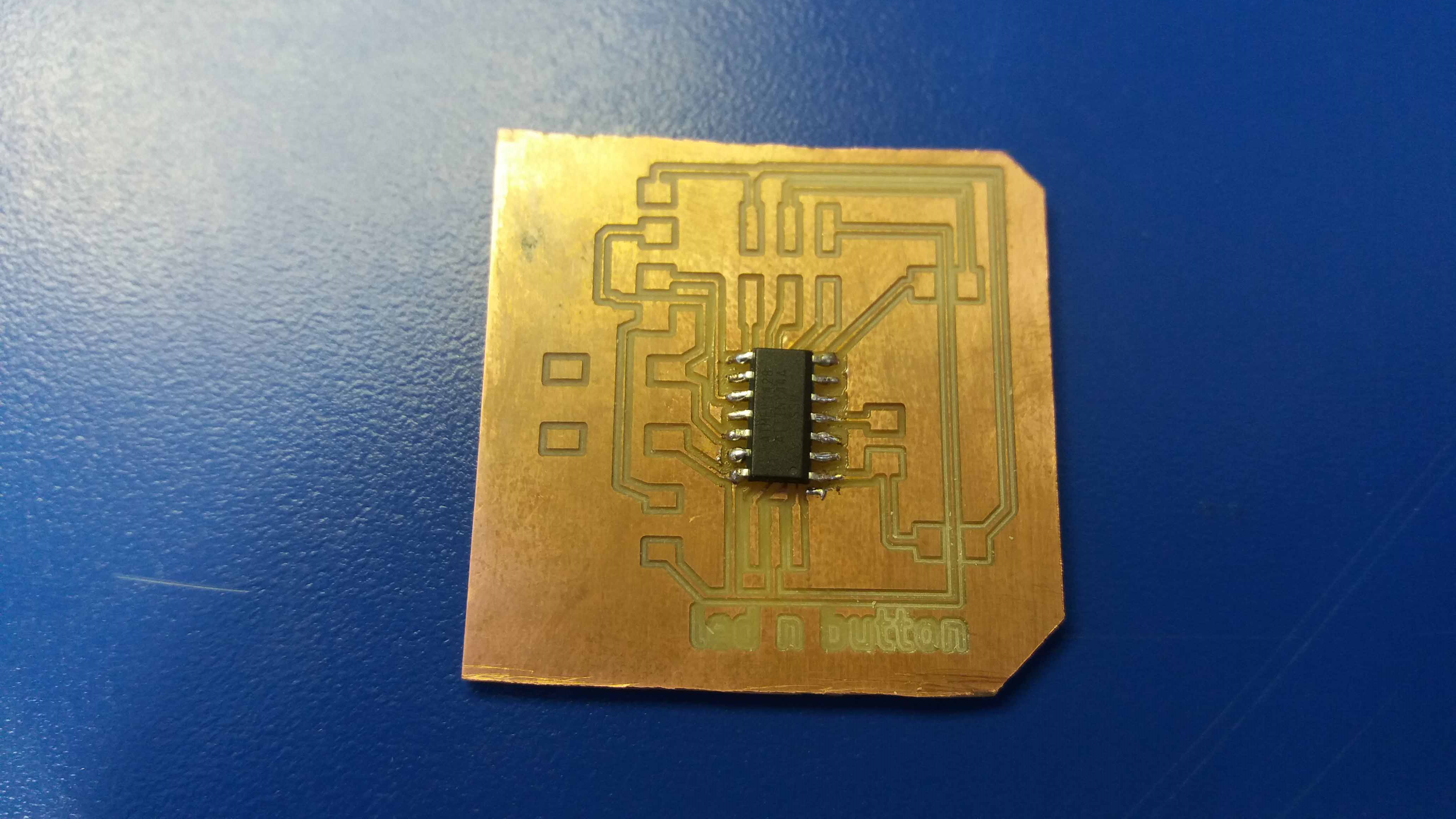
I though the construction was pretty tought, and actually did resist some preasure with the programming cables, but it finally broke. Then, I decided to fabricate a new board with the led and the button integrated. I will try to save the previous chip in the future. In the meantime, here is the "led and button" design and fabrication.
Design Software
Kicad
Kicad was explored. This is a open-source program very versatile, but the learning curve is harder than the paid, Eagle option.
For learning, the tutorial "Getting started in kikad" was used. The link is in pdf format. Pay special attencion to the workflow, in page 5.
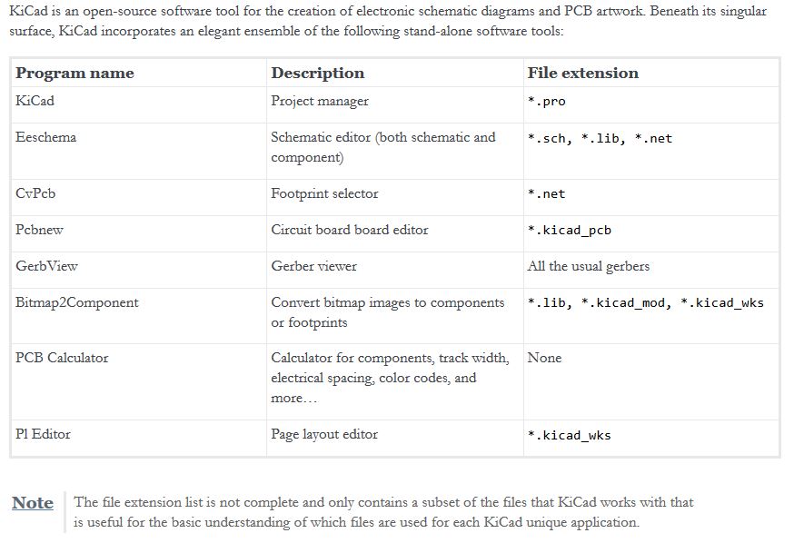
The program have subcomponents. Here they are, with their descriptions and file extensions.
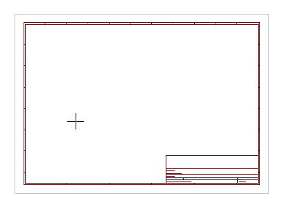
After creating a project, we start creating our schematic using the EESchema program/tool. That present us a blank page.
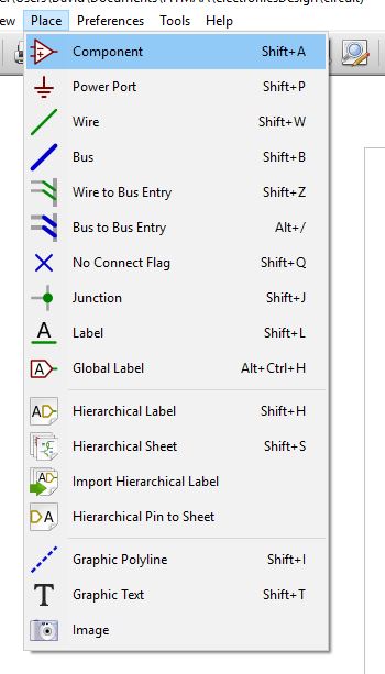
Then, we start to adding components using the component command. Using shortcuts speeds up the workflow.
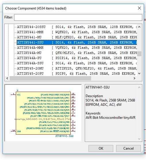
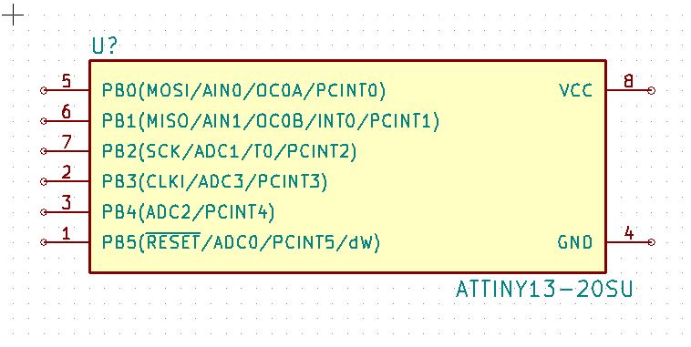
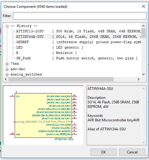
From the list, we choose the microcontroller that we are going to use. We have also a preview.
Then, we place it on the working area.
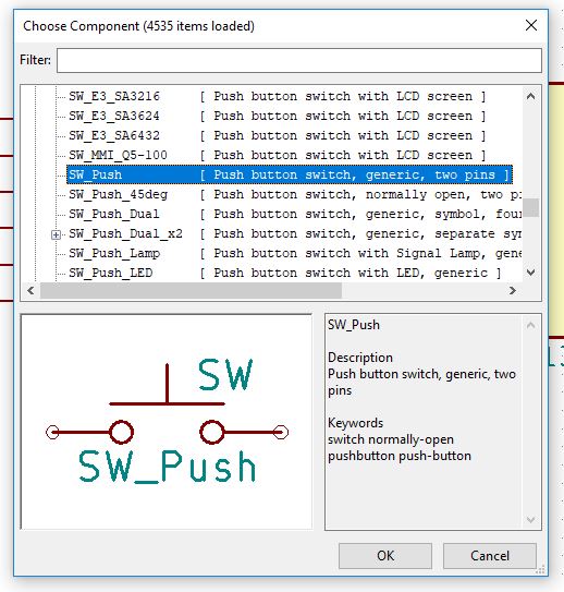
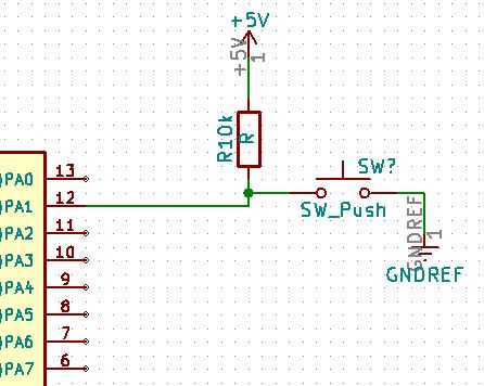
We continue adding elements. Here we have the push button.
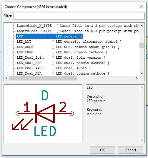
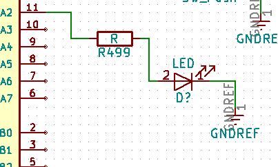
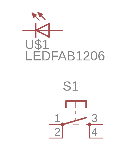
And the LED:
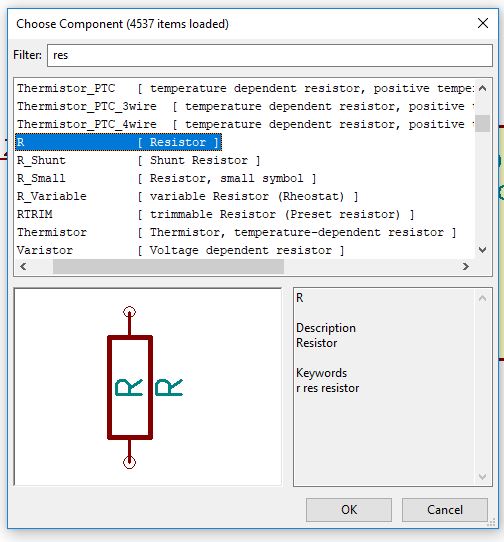
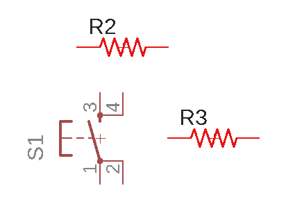
Following with a resistor.
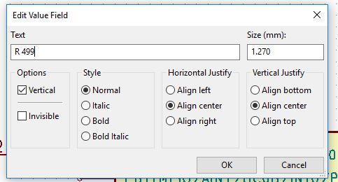
With a right-click, we can add it's value. This could also be done later.
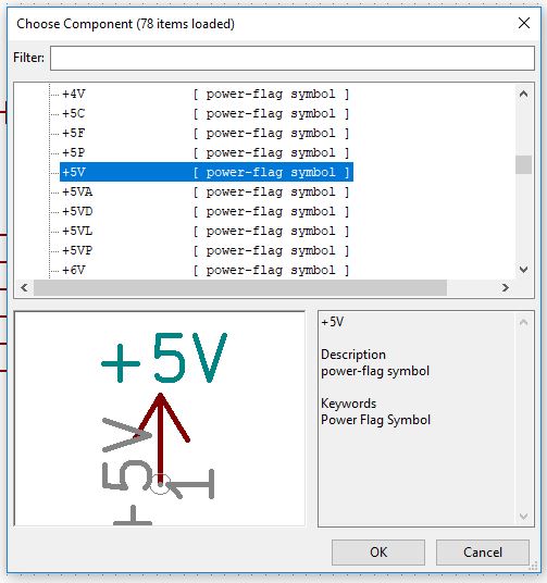
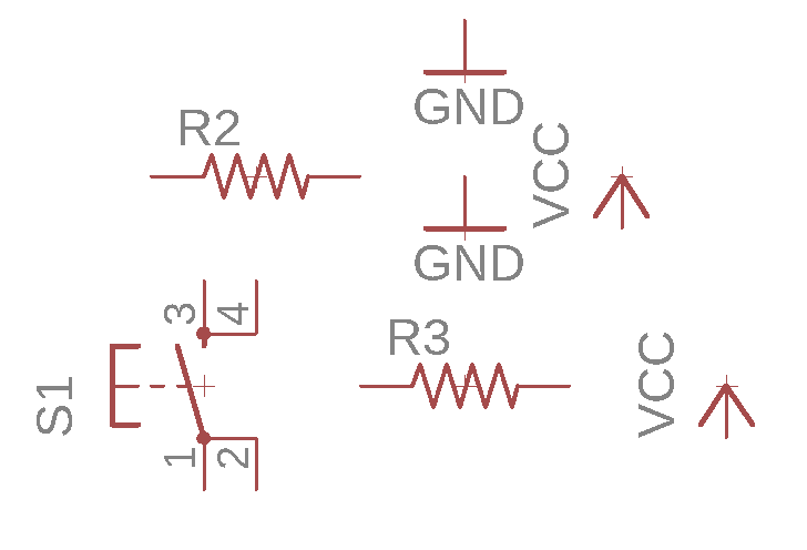
We continue by adding a power flag, in this case, a +5V one.
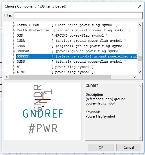
Then, a ground power flag.
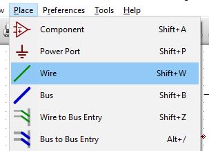
In the tab "Place", we find the wire tool. We also have it in the right panel, and it is posible to use the "W" hotkey too.
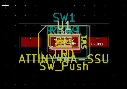
I decided to change the processor. Here is the new one.
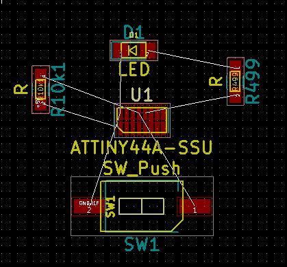
With all the components in place, I arrange them in a desired position, and started the wiring process. Here is the switch part.
And here the LED part.
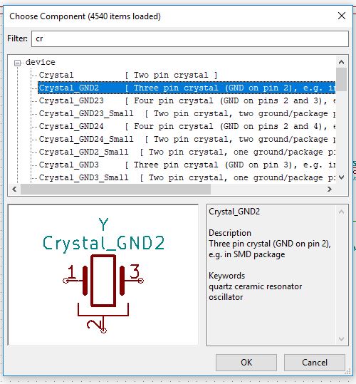
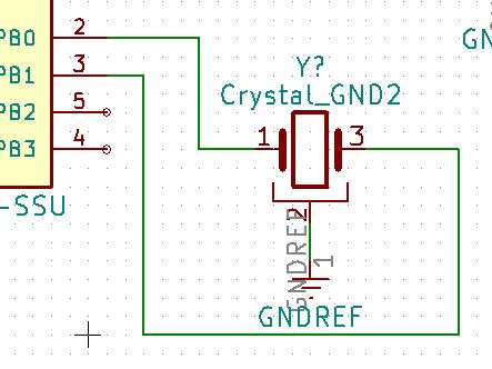
Also, I added a crystal.
And wired it up.
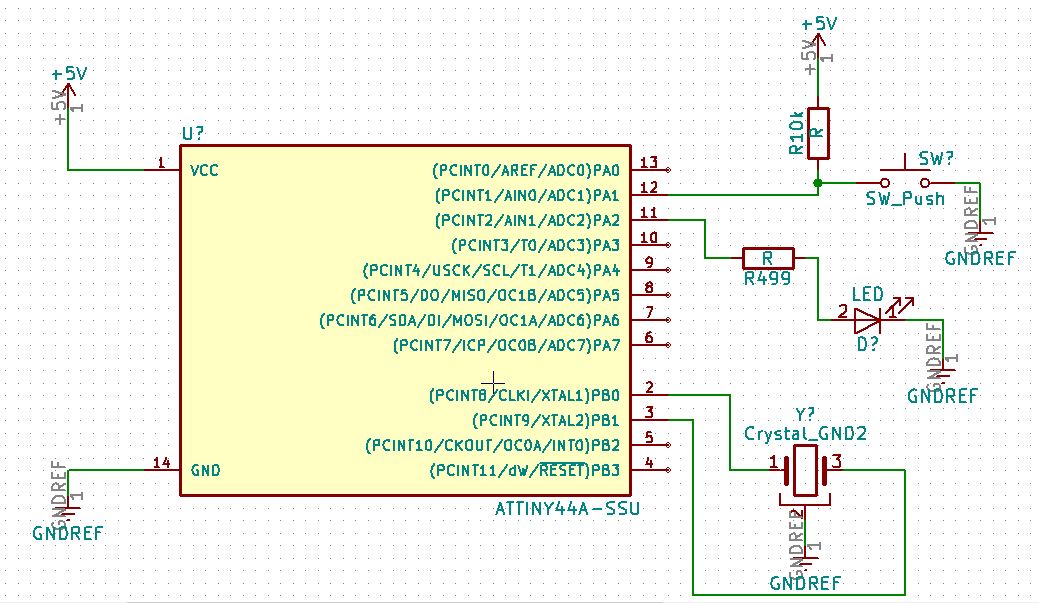
Here is an overview of all the elements, placed and wired.
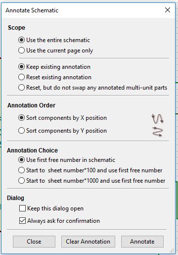
The next step was to annotate the skematic. This is done using the "Annotate Schematics Components", in the upper panel. This tool gives names to the components (or numbers, to be exact), making them unique and replacing the ? signs placed by default.
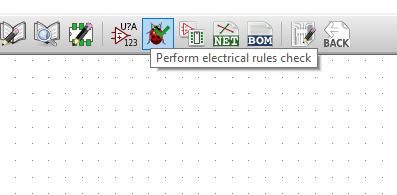
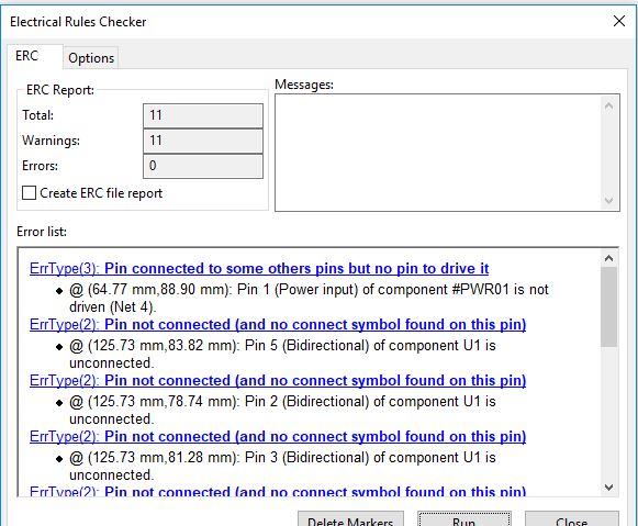
Then, we perfom the Electrical rules check using the button in the upper panel.
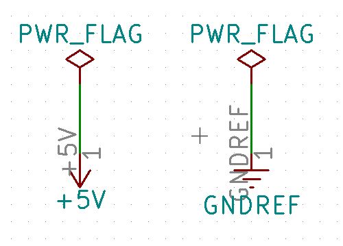
That give us 11 errors. After some research, I found I needed a explicit power flags.
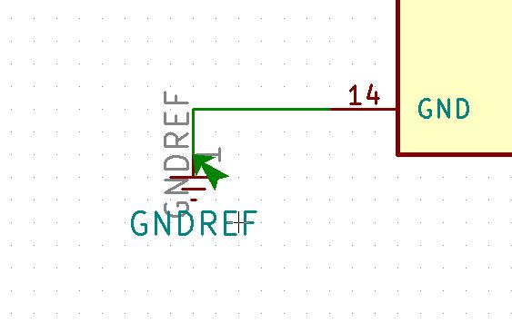
The marking of the problem with a green arrow indicates where the error is.
I added the power flag, and repeated the check.
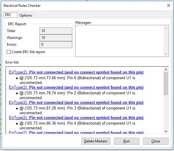
The error was reduced to 10.
I found in internet forums that we needed an X to indicate the pins that are not connected. This flag can be found in the right panel. Kikad, contrary to Eagle, needs an explicit indication of the parts of the circuit that are not connected.
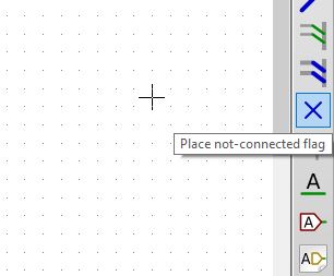
Then I conected the flag to a pin, and test it...
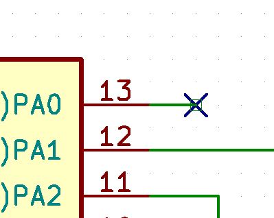
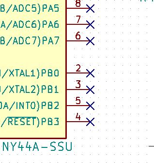
The error was reduced to 9. Then I connected all the remaining nine pins to an X flag. I discovered that it was posible to connect them directly, without the need of a wire.
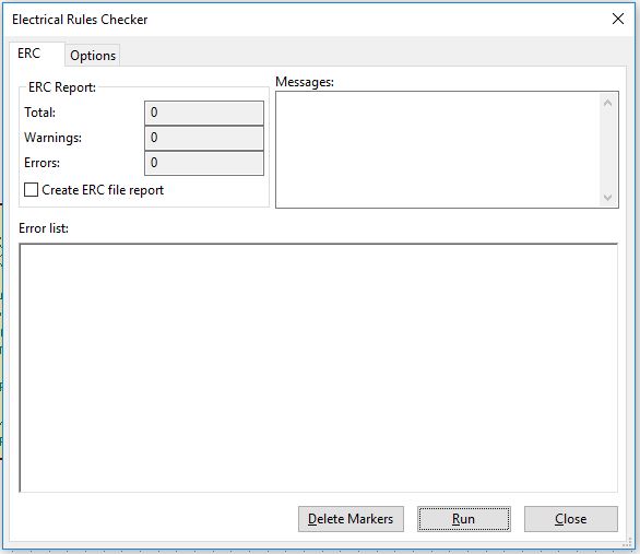
When the test was perfomed this time, the errors were cero.
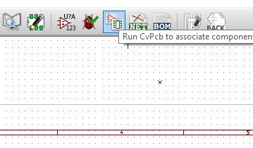
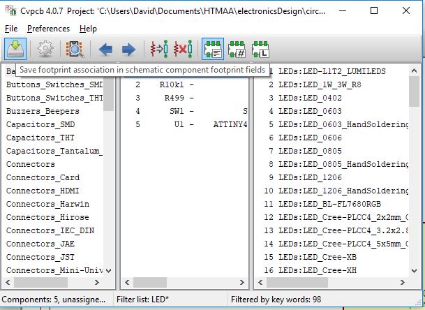
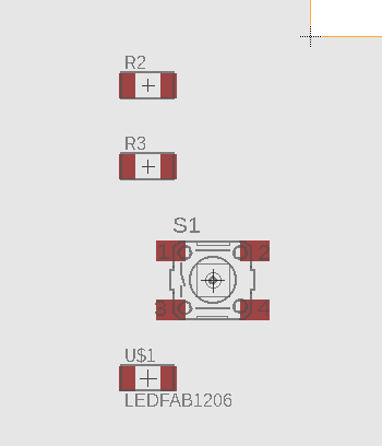
Before continuing, it is necessary to run the CvPcv tool. This associates the components symbols writen in the schematics with footprints, with the actual meassurements of the components. In this point, if they don't exsist in our libraries, we can create our own. This will not be covered in this demonstration.
This will list our components, along with too lists. On the left, we have the type of component. On the right, the components themselves. From them, we choose the ones that corresponds to our stock components.
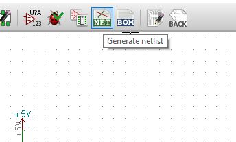
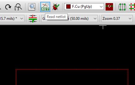
In this point, we generate the netlist. This file will be used to locate and connect our components in the working area.
After this file is generated, we can click in the Pcbnew, from the program main control.
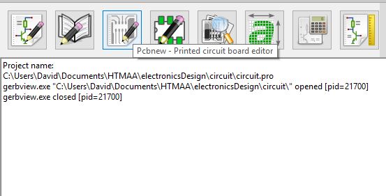
And an empthy area opens.
At this point, we can check our design rules using the Desing Rules Editor.
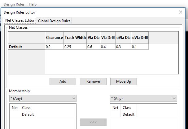
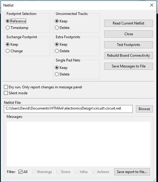
We check it and close it. Then, we read the netlist we created before.
We check the parameters and click on "Read Current Netlist".
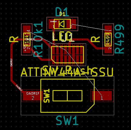
Then, we can see all the components clamped in the center.
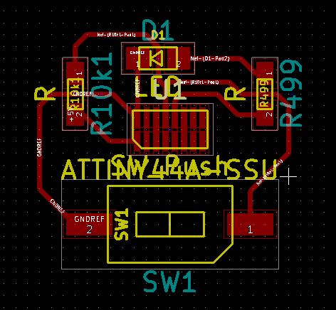
We move them appart to see them clearly, with their connections (rastnet).
Then we locate them appropiatelly, and proceed with the wiring. We can use the "W" hotkey, or the buttons/context menu. To close the path, right-click on the final point and choose "end track."
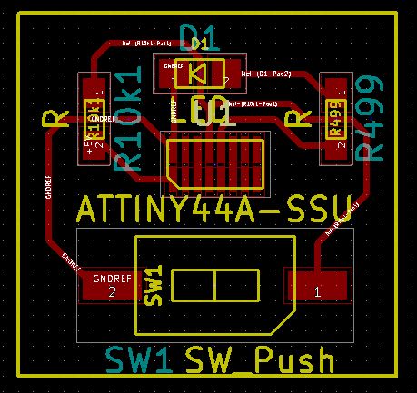
This is the wiring, completed.
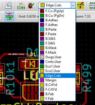
For the border, we change the layer to Edge cuts...
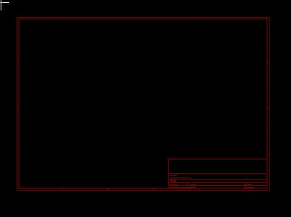
And draw a square/rectangle defining where the board has to be cut. I also moved the text, so it is visible and more aestethic.
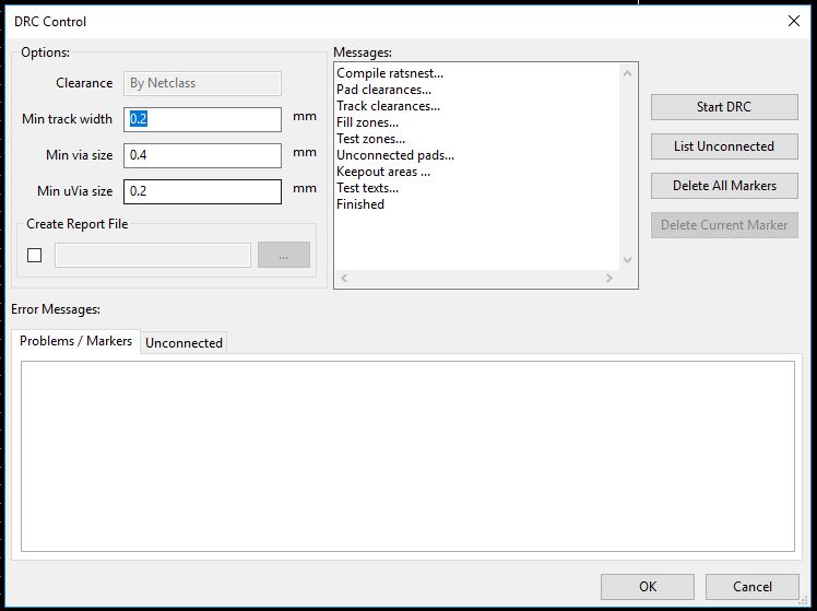
One of the final steps is to perform the design rules check.
If no error appears...
The board is ready to export to Gerber files or to FabModules. One of the interesting features this program has is the 3d View of the board. Some people find it useful, and personally I think it could be used in presentations.
In conclusion, I found this program very useful, with the plus of following the open-source phylosophy. The downside is the learning curve, that I found longer than Eagle, and the problems in the export formats to prepare the files for the Fab Modules system.

The files for this design can be found here. Kikad installed in your system is required to open them.
Eagle
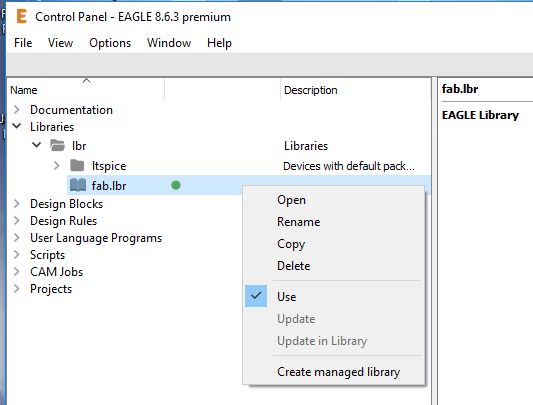
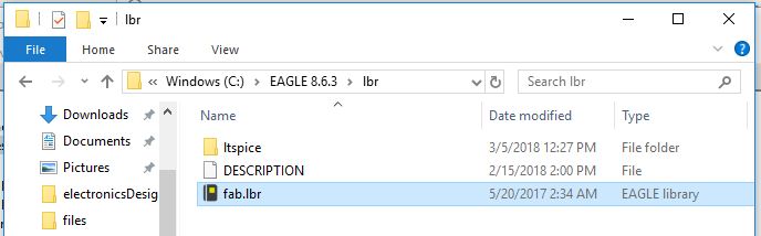
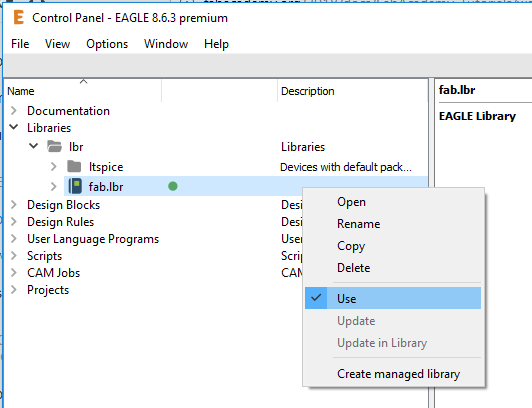
After downloading and installing Autodesk's Eagle program, we have to install the fab library.
Preparing the fab.lbr installation:
This error returned:
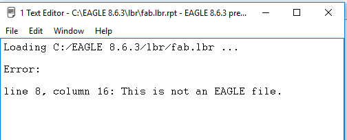
I downloaded all the folder (and unzziped). Then, it worked fine.
Last part. Tell the program to use the library:
We open the file hello.fdti.44 with Eagle:
We can start to add some components. We are going to start with some resitors. Then, we add a switch:
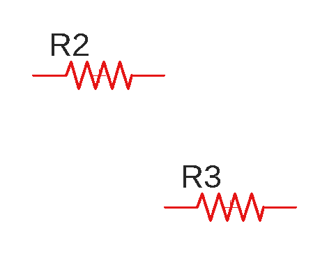
We add the rest of the components, and finally, the led.
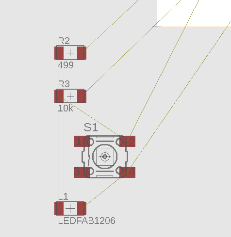
If we switch to the board view, we can see the new components, not linked and out of the working area.
Then, we proceed to connect the components with lines. We connect the ground, and label and value our components.
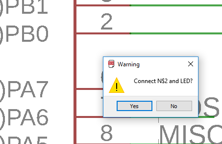
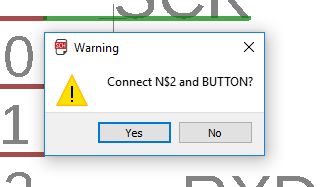
Notice that we labeled the right part of the circuit (net) with a name LED. We are going to name the pin #6 on the processor the same, so the subcircuit is conected to automatically to it. When the programm asks us to confirm the conection, we do it so.
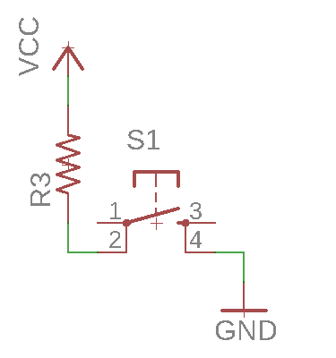
The led (output) part of the circuit is completed, with it's current limiting resitor. We do de same for the input subcircuit (button), this time with a pull up resistor, that disambiguates our signal and avoid false negative readings and annoying incosistency. We name and label the green part of the net that is going to be connected to the input pin (in this case, pin #10).
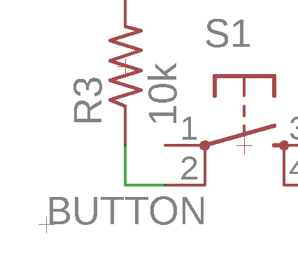
Naming the pin number 10 BUTTON, the system ask us to confirm the connection. We proceed. If we switch to the board view, we can see the components, this time linked, but still out of the working area.
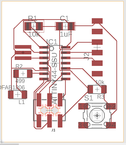
Then, we create our first layout attempt:
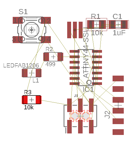
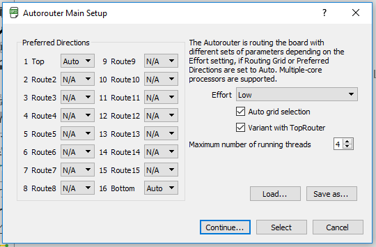
We explored the autorouting tool:
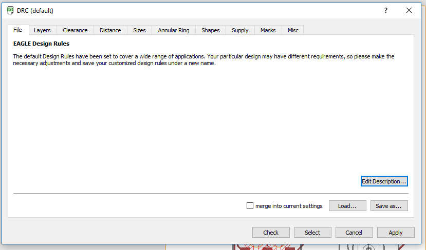
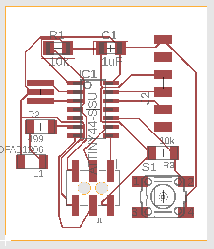
And the DCR system, to check that our design rules comply with the design:

And finally we export the desings in png format, exporting the layers that we need. Now the files are ready to processing and milling.
Assigment update
At the end of the day, the previous board was not milled. We noticed that the paths where too thin, and some of them where also too close together.
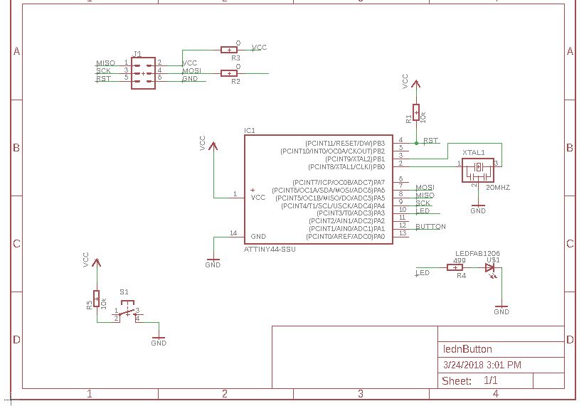
I started a desing from scratch and manually. For keep it simple, I didn't include the FTDI connection. It resulted in an error for programming, as it didn't have a power source. I had to provide the power externally and then it worked fine. The lesson here is: Always check that your device is well fed. Here is an overview of the schematic.
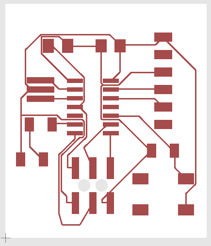
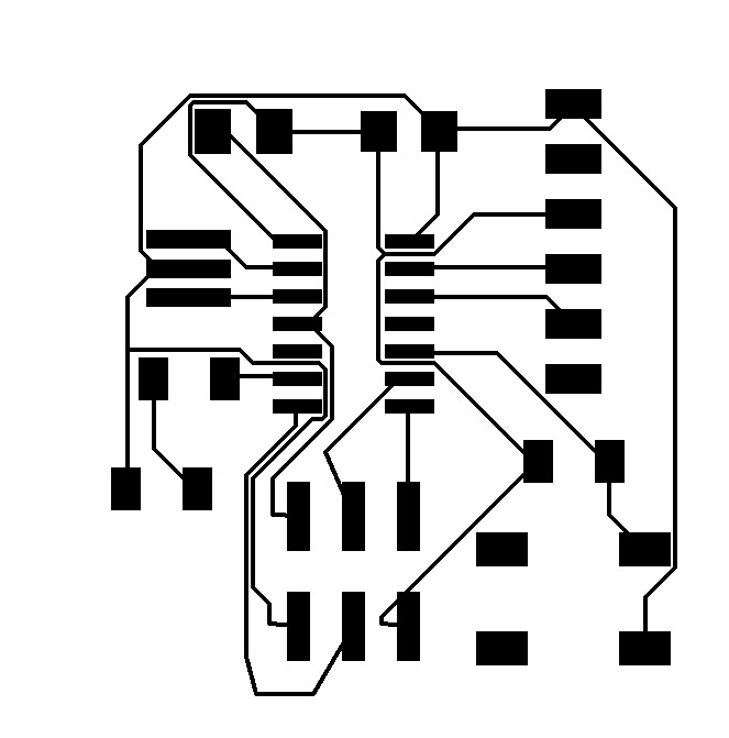
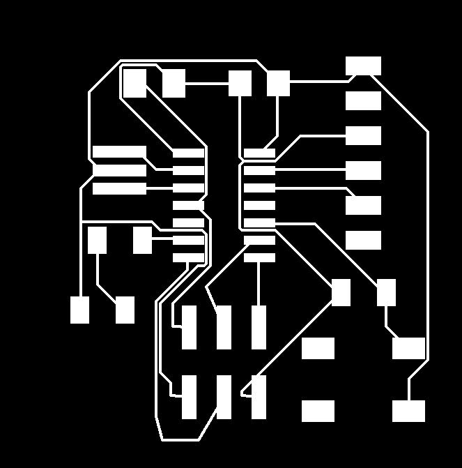
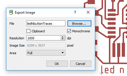
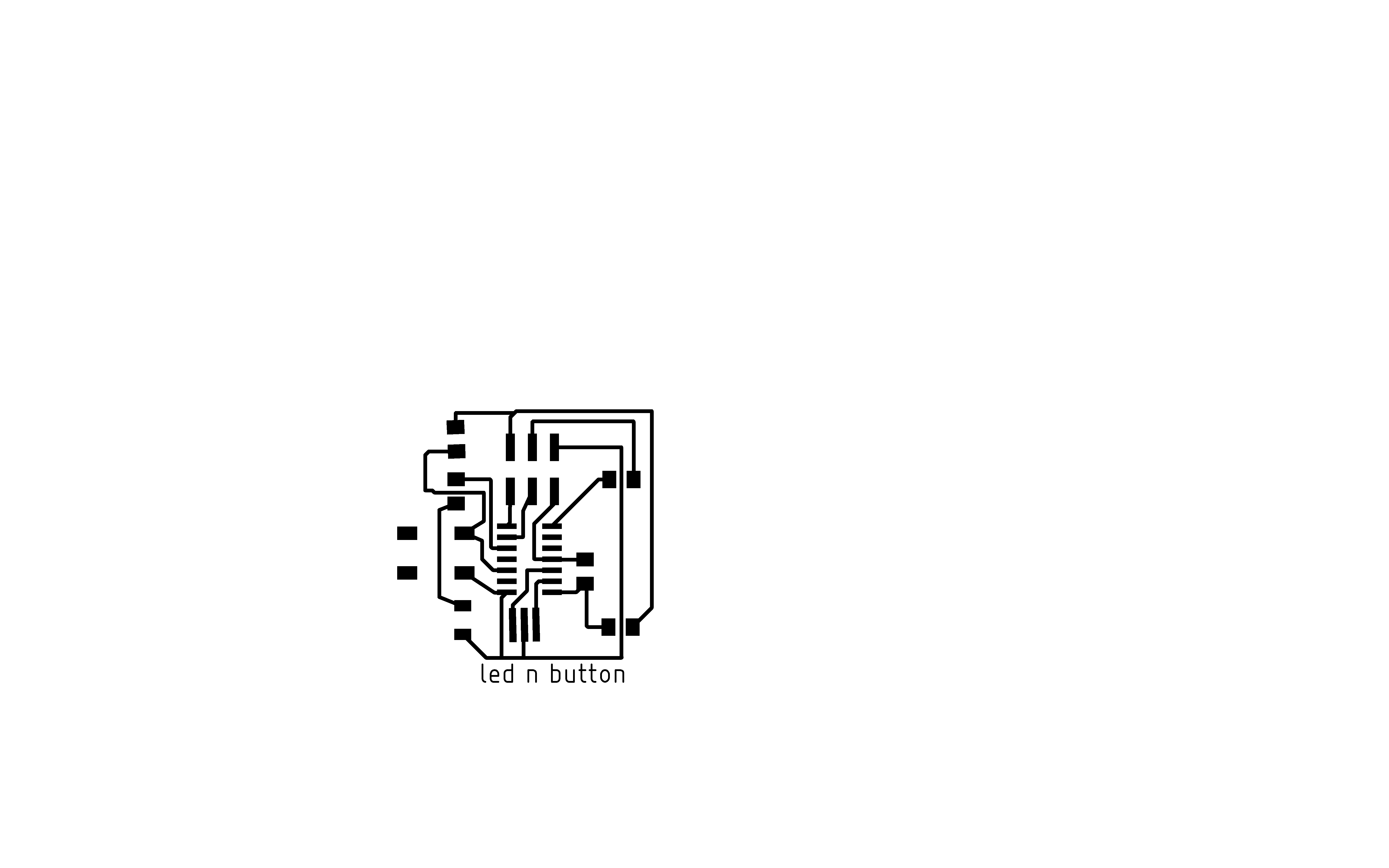
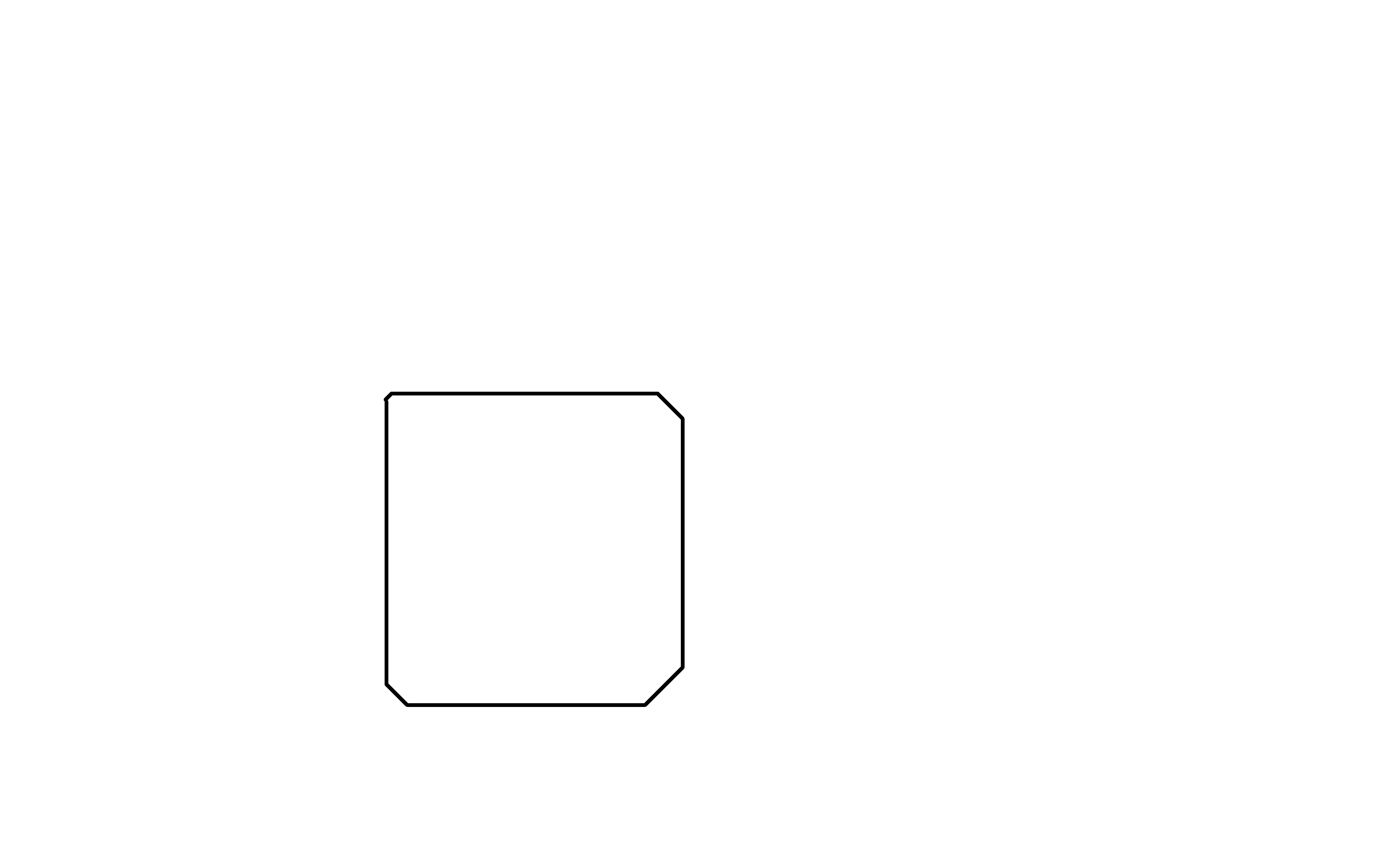
And the resulting board.
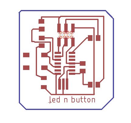
We export the design with high dpi ratio (500 dpi or higher recomended. We used 1000 dpi).
Here are the files that can be used for milling:
In conclusion, I found Eagle easy to use, and the export feature was very useful, specially for Fab Modules use. The downside is that it is a paid version, and requires an investment only necessary if the board design will be used constantly. Still, I this it is necessary to experiment more with KiCad, Eagle, and other softwares to have a more educated opinion.
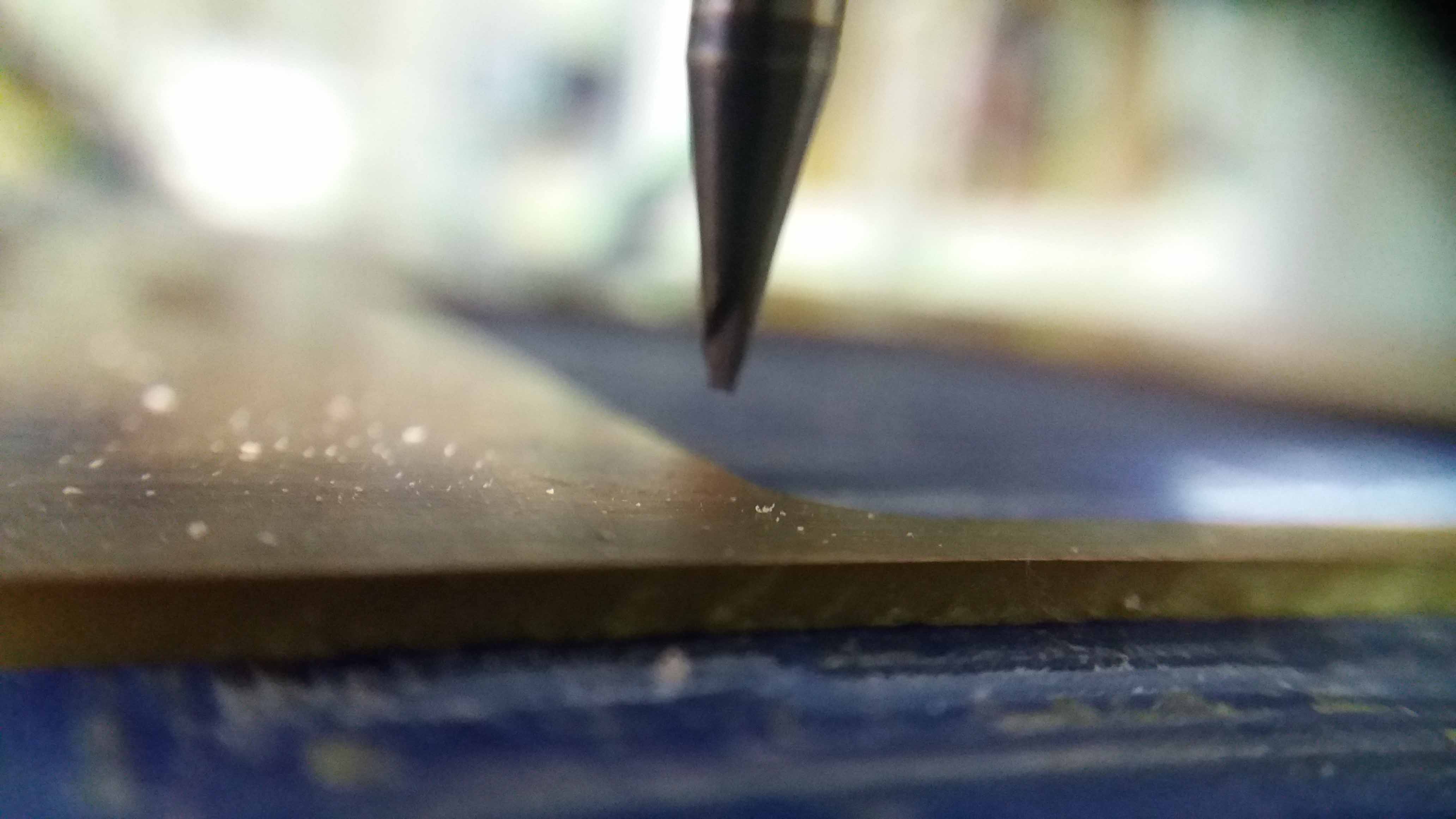
Update: After a few weeks after this attempt, we change the tool and the cutting was a lot better. It seems that the tool was old/not well maintained/poor quality. Also, the setting was made incorrectly, aiming to a single pass. Unfoutunatelly, I don't have a record of the wrong settings.
Here, we can see the milling test perfomed whith the new tool. The quality is much better. This allow us to be more thight with the design rules, and to obtain better results.
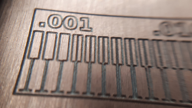
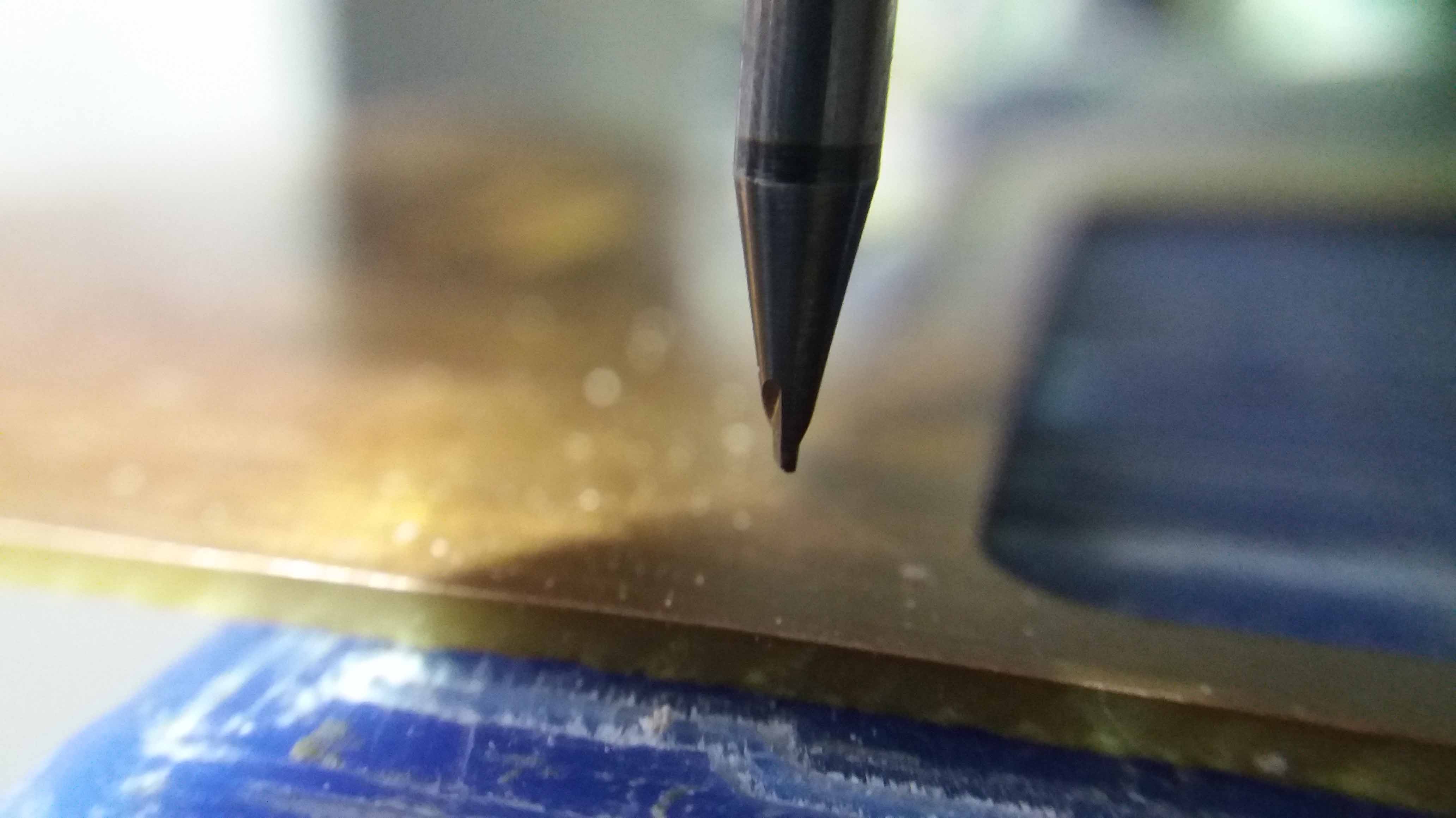
In this first image we see that, at .001 distance the traces are milled away. This means that we have to set the rules to a wider distance, otherwise we will loose our traces.
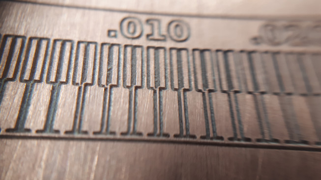
At .010 distance we see that we conserve our traces. This might be an appropiate setting.
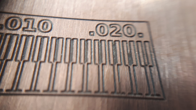
At .020, still our traces are conserved. The problem with larger widths is the posibility to accomodate more elements and the need of more complex paths and bridges.
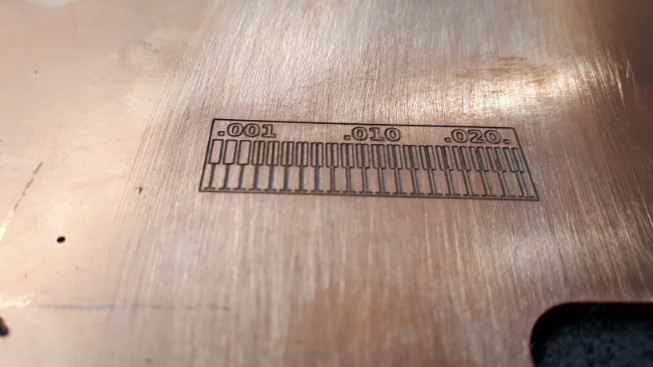
Finally, here we have an overview of the complete test/board.
Once exported, the milling process was perfomed.
Unfortunatelly, the tool broke in the middle of the border cut.
This is the other side of the board. The channel is saturated with material.
With the new tool we made the test, and the results look noticeable better with the new tool. We can see them here:
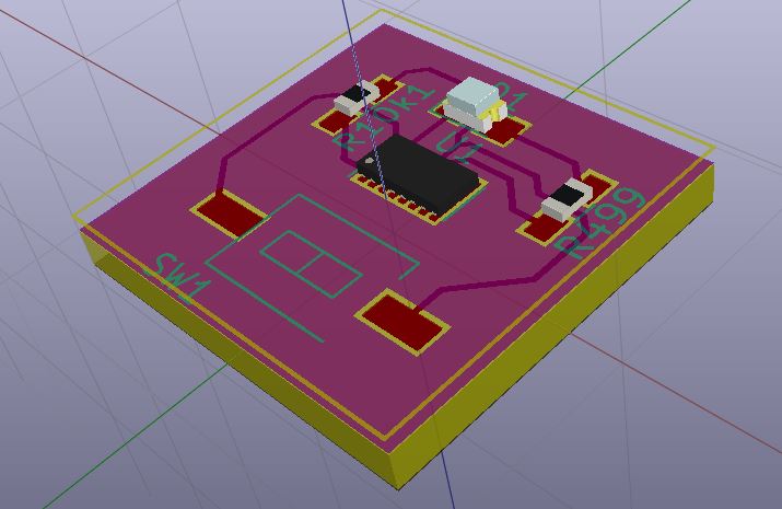
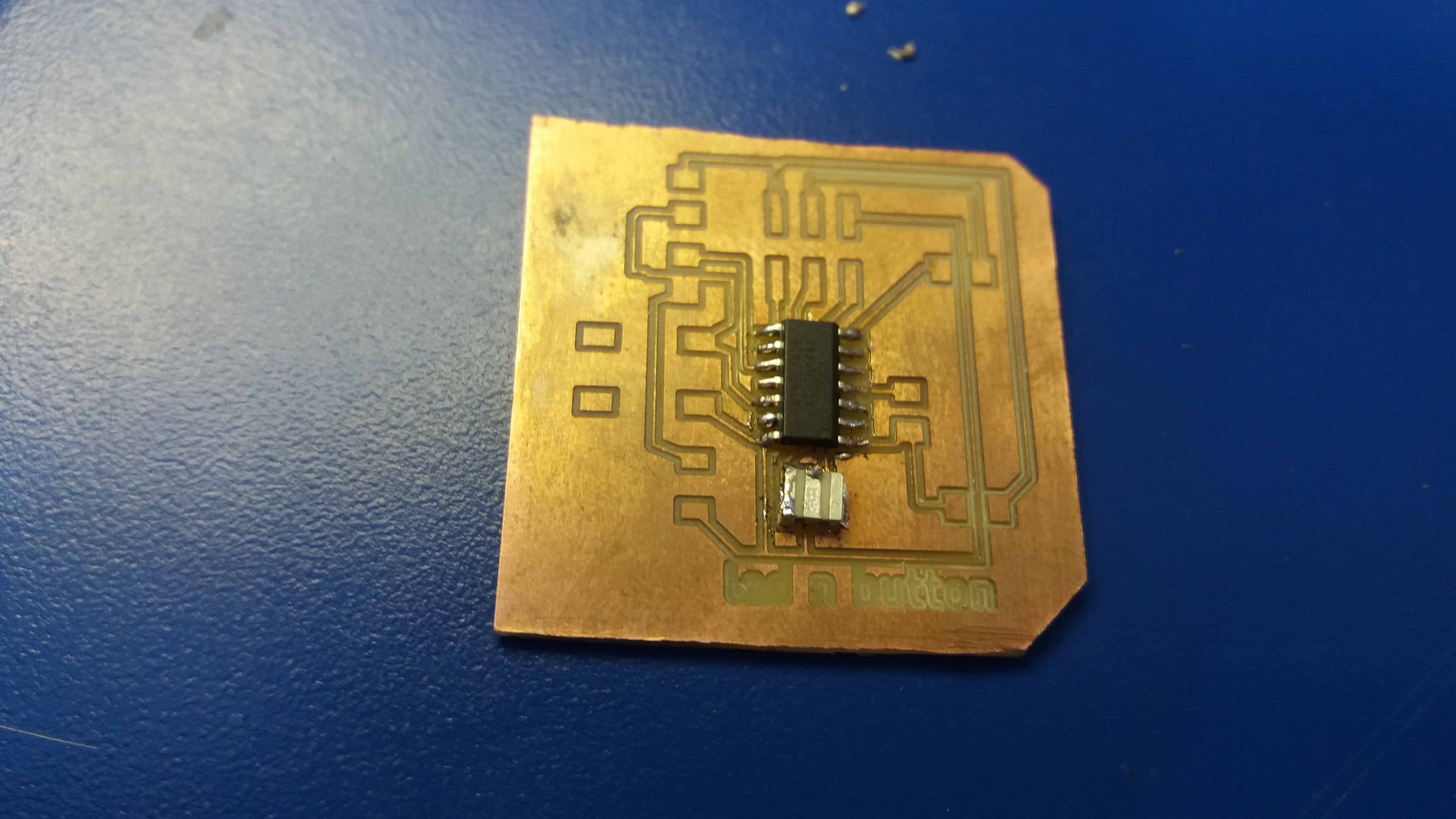
At the end, I had to cut the rest manually. Here follows the board cut manually and with the microcontroller and the cristal/resonator soldered.
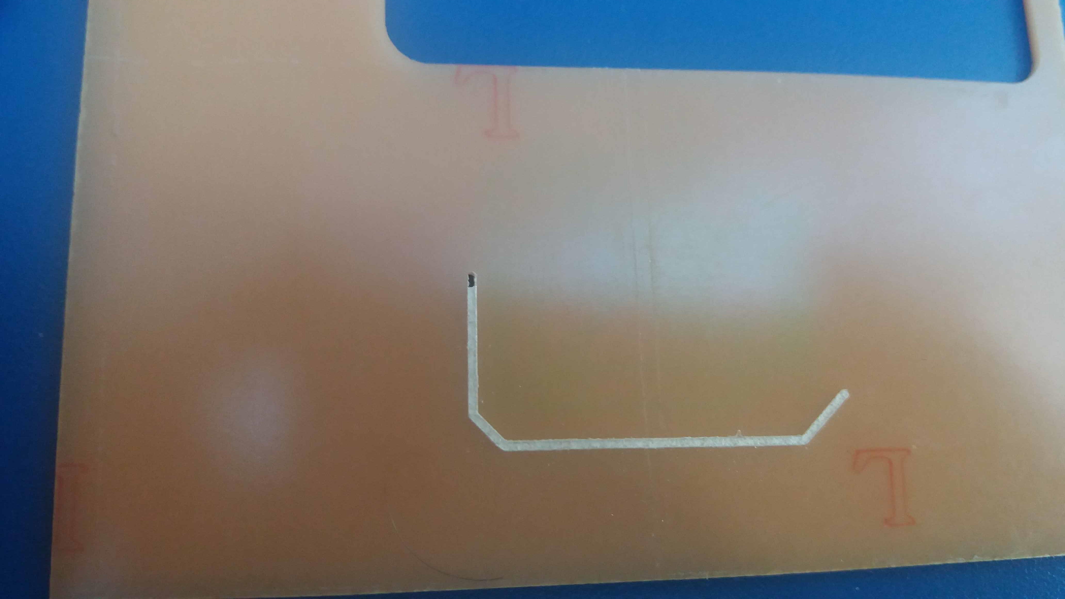
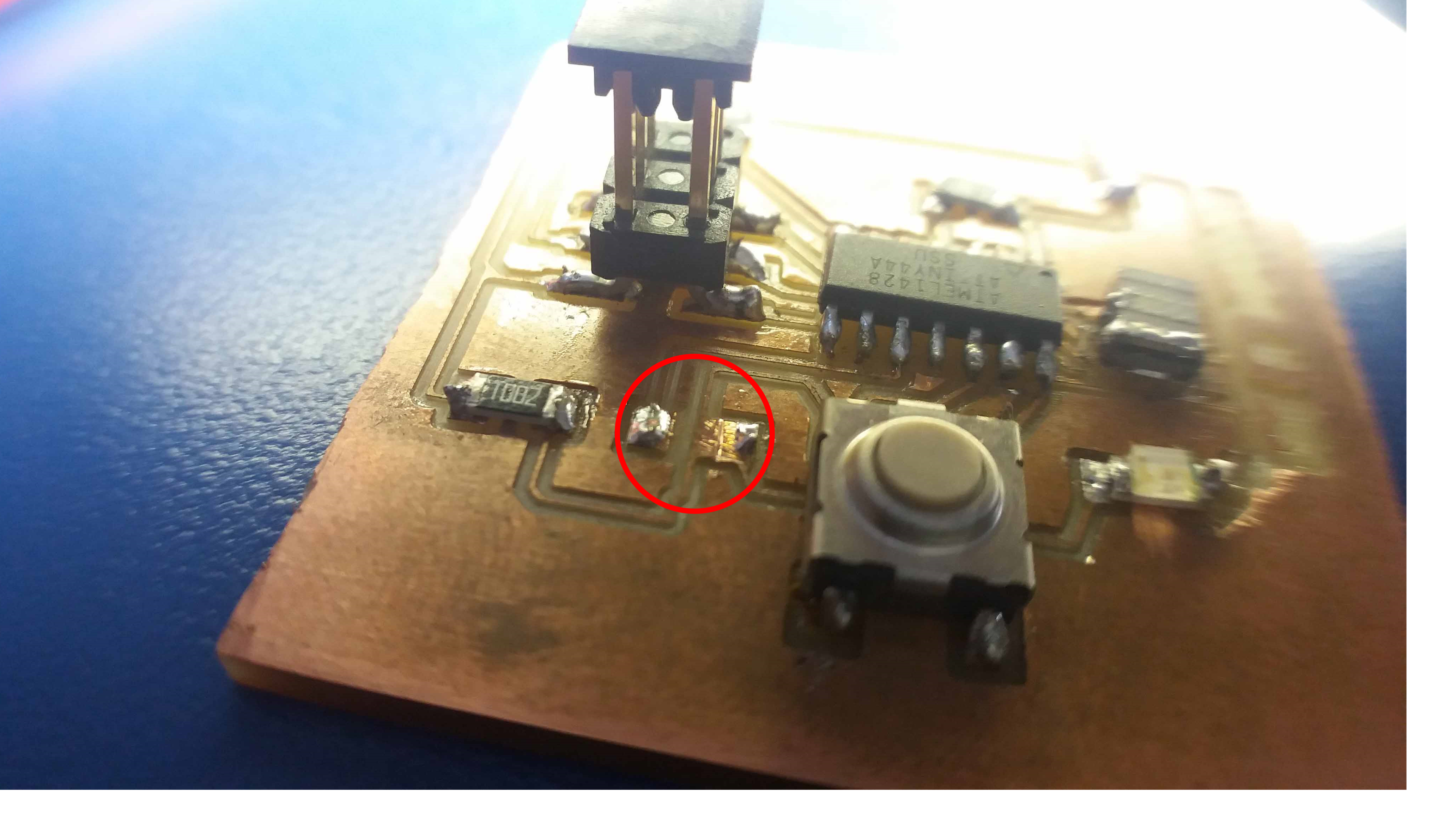
In the first picture following this lines we can see the board with the button incorporated.
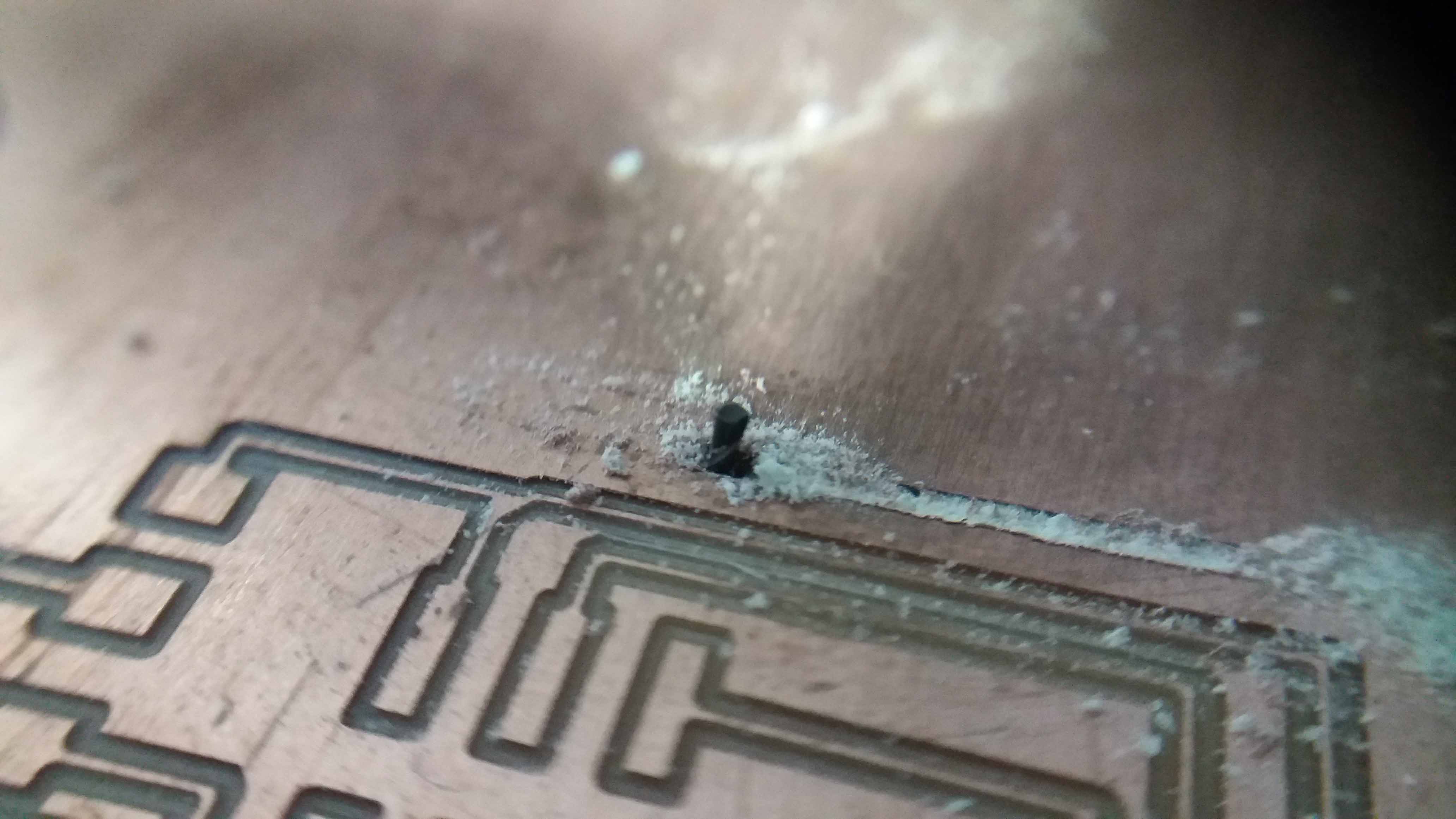
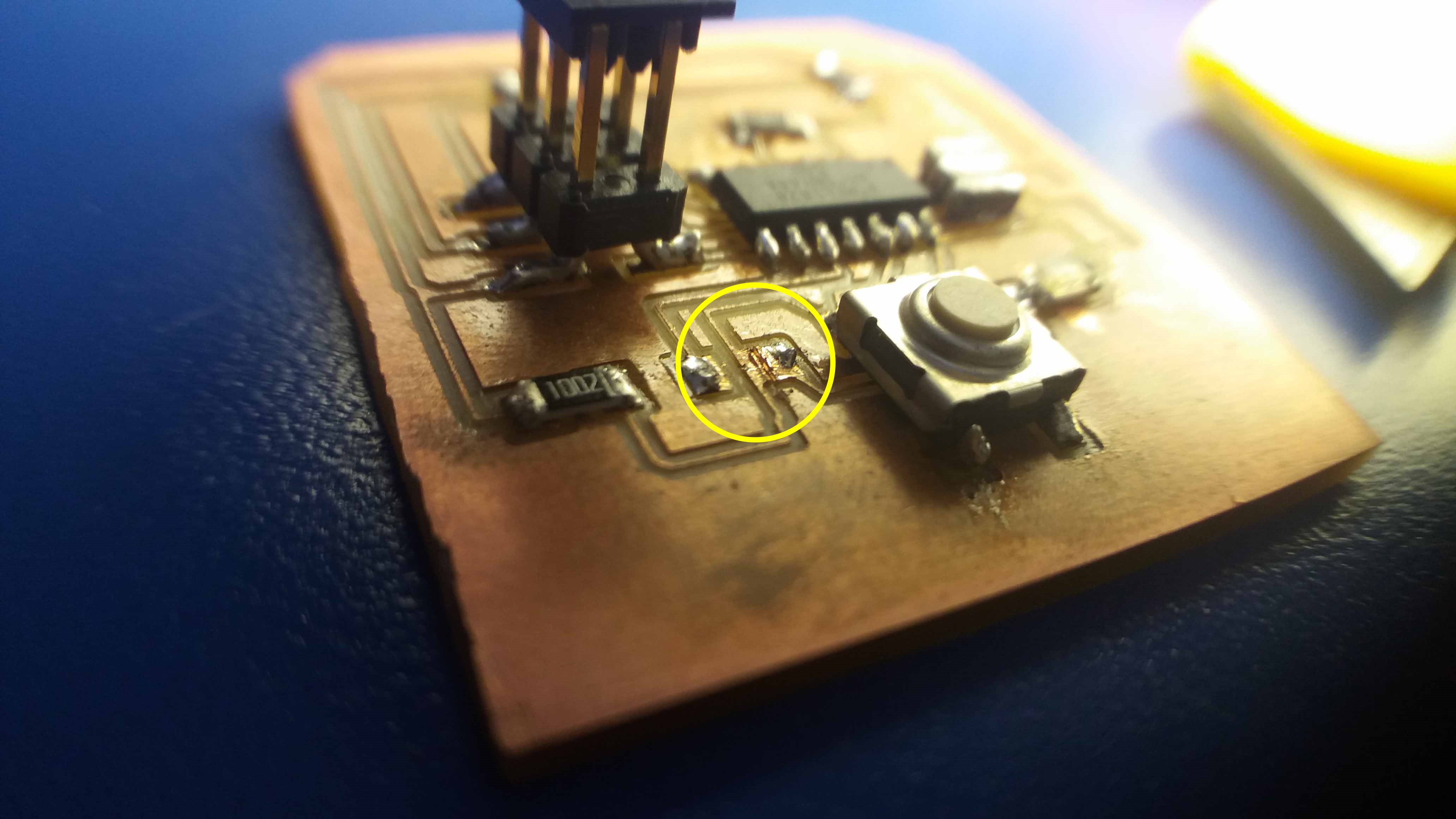
After inspection and testing with the multimeter, I found there was a unwanted connection marked with a red circle in the picture. I actually had to desoldier a resistor that was on the way. I used a knife to cut this undesired connection (shown with a yellow circle).
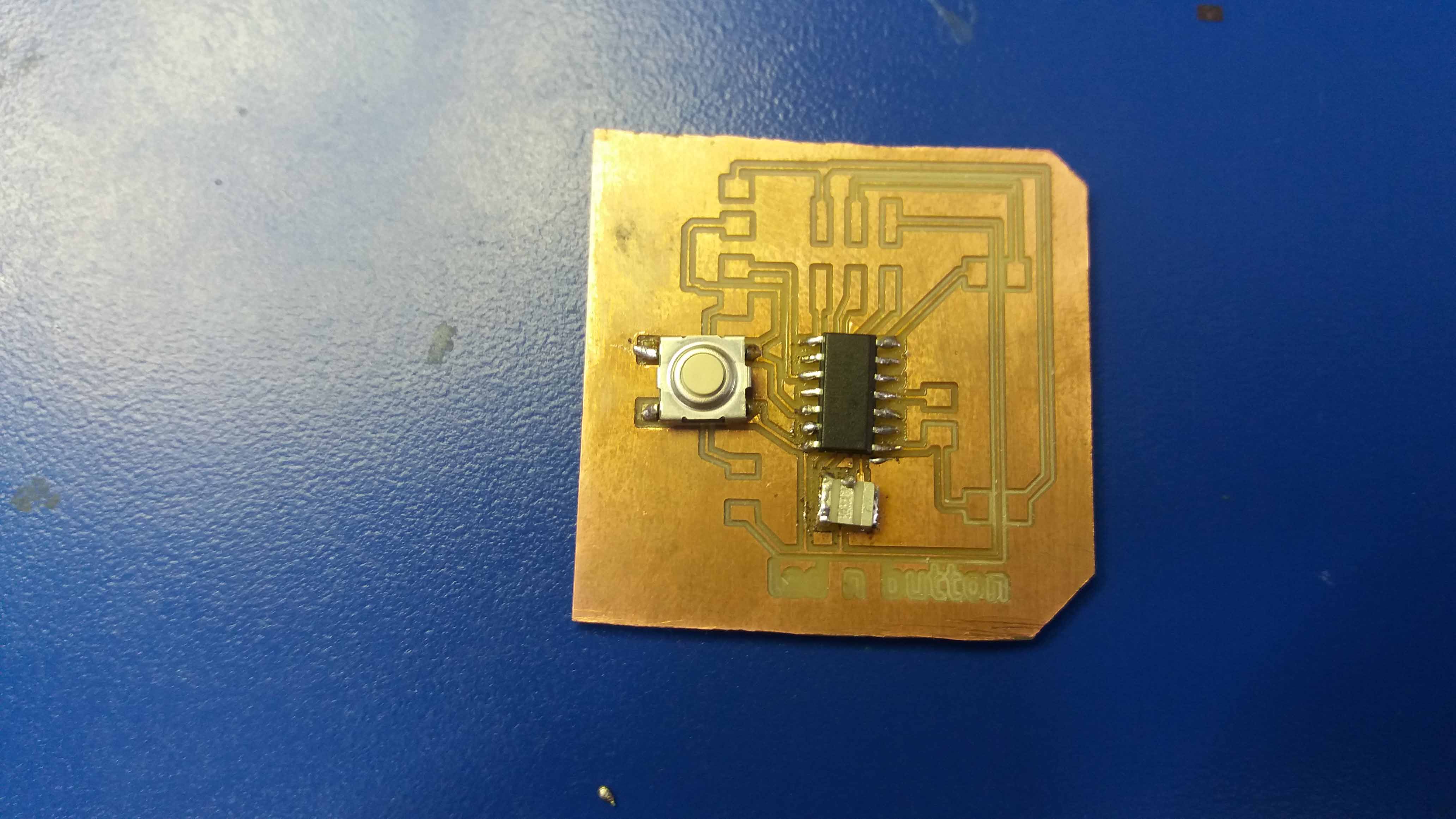
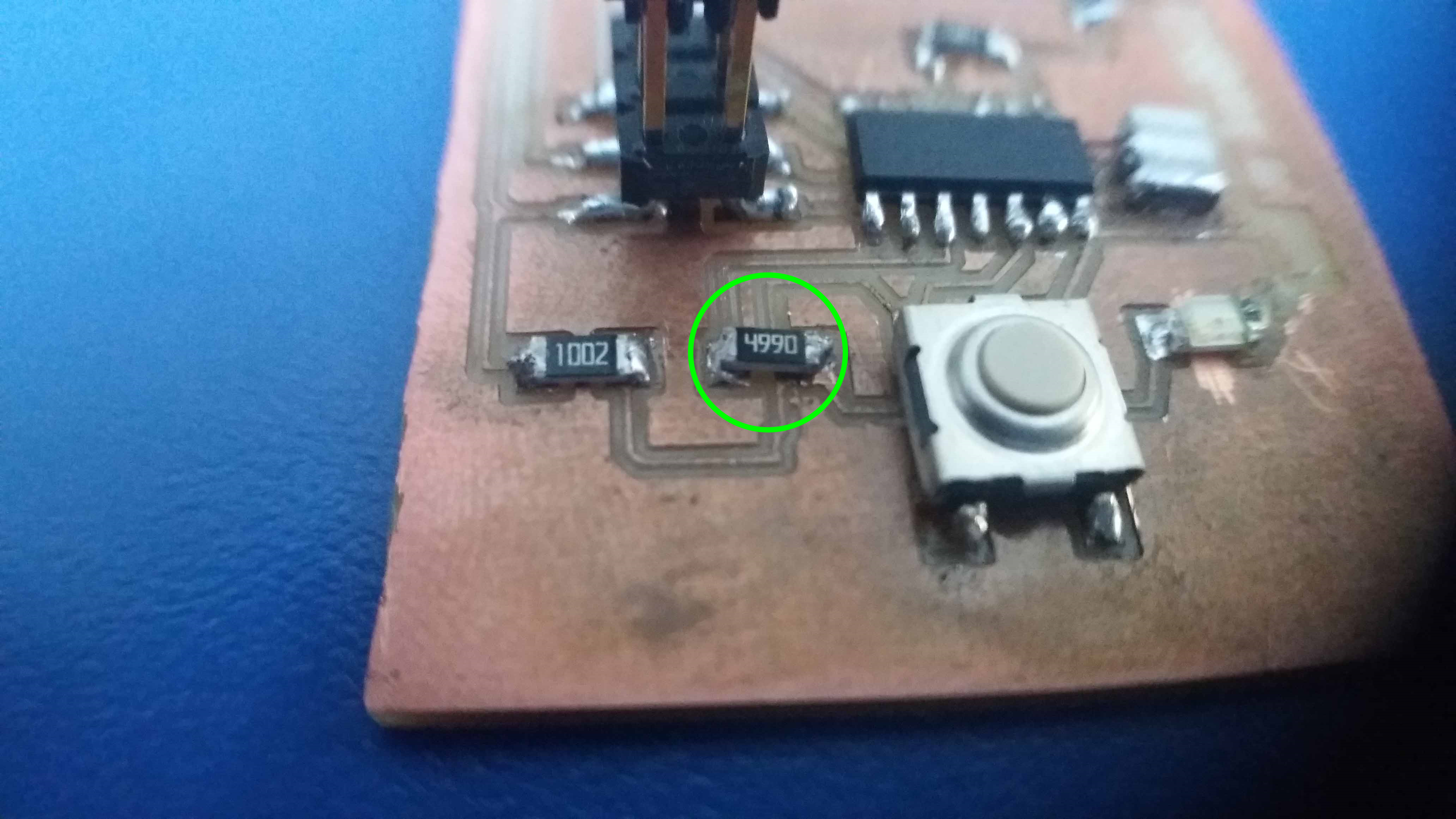
And place the resistor in place (marked in green). Finally, the board is ready to be programmed.
The arduino programming language have two parts. One, "Setup", runs once, "setting" things up. Then, the "loop" function executes continuosly.
Here we can see that in "Setup()" we inicialize the pin 3 as an output. Then, in the loop, first we write digitally (0 or 1), the pin number 3 as a HIGH (or 1). It means it lights up. Then, we set a delay() of 500 miliseconds (half a second), for keeping the led light ON for that time. Then we digitally write in the pin 3 a LOW (0, or OFF). We keep it that way for another half a second, and start the loop over again.
Here is the sketch where, upon button pressing, the LED is off for one second, on for another, and off again.
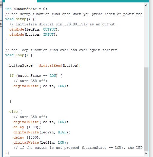
Here we use a conditional. "If", the button state equals off/LOW (note the double equal sign. Just one means assigmet of a value to a variable), the ledPin stays LOW. On the contrary, if that's not true (aka, the button is pressed), the else subroutine executes, so the LED (defined here as LedPin), turns off for a second, then high for a second, then low again. Then repeats continouslly.
The following sketch turns the LED off when the button is pressed:
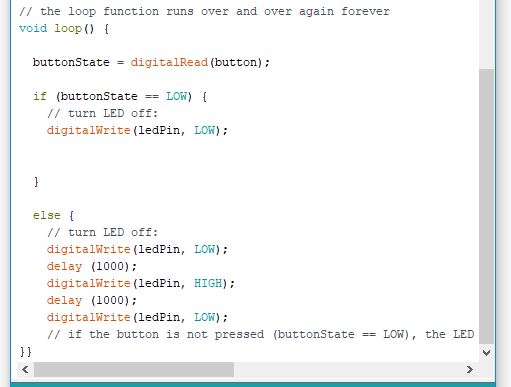
Here are other examples. First, we declare global integer variables as ledPin = 3; (for the number of the pin assingned to the ledPin variable), a button with the assigment of A1 (analog 1), for the button input. Then, in the setup, the LED and button pin are assigned as a OUTPUT and an INPUT consecutivelly.
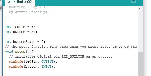
Then, in the loop() function we read the state of the digital INPUT (0 or 1, on or off) and assing it to the variable buttonState. After that, we have two choices, LOW or HIGH. If the button is not pressed (digitalRead LOW), we write digitally the ledPin LOW. If the button is pressed, an alternation occurs, with 1 second intervals.
The board, schematics, and programs (sketches) can be found here:
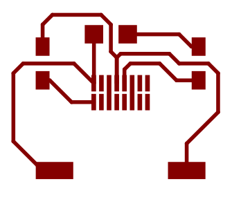
Led and button schematics
Led and button board
Blink original LED in pin 3
Blink
Config 1 LED and button
Config 2 LED and button

This work is licensed under a Creative Commons Attribution 4.0 International License.