Tasks of this week:
The weekly assignment started with the simple tasks:
Starting with the Simple three tasks.
1. Group Assignment:
use the test equipment in your lab to observe the operation of a microcontroller circuit board.
2. Redraw the echo hello-world board add (at least) a button and LED (with current limiting resistor)
check the design rules, make it, and test
1. group assignment:
The group assigment for this week was to check various tools, which display numerous properties about electrical components. The components we have in our lab, and their functioning goes as follows:
Oscilloscope:
Oscilloscope is a device for viewing oscillations by a display on the screen of a cathode ray tube. For this we had tested a hellow world board.
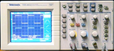
For this test the helloworld board was connceted to the laptop where the ocilloscope was connected to the communication pins of the board, and the board was connected via a programmer to the PC, We measured the signals of pins that was connected with the oscilloscope.
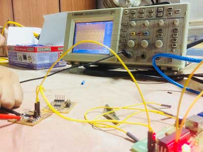
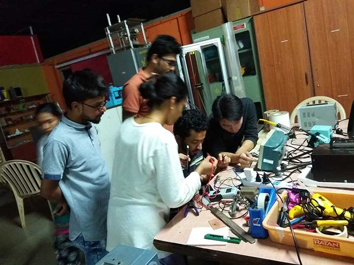
For the initial we were quite guided by one of our colleague, Rutvij Pathak, and one of our instructors, who being electroninc enginers had previous experience with the tools.
The wave is actually supposed to be in the form of pulses, but rather it appears to be sinusoidal, it's because the soldering was not perfect on the position where the oscillator was attached.
Multimeter:
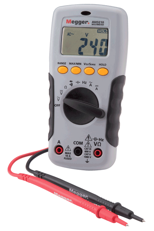
This is a device probably available in every lab it has mutiple function as the image describes.. We used it to check the polarities of the LED, ressitance and capacitance and the continuity of the circuit board
Eagle
Learning Eagle was not that easy as I thought. Though I used it in few assignments.This is how it looks.
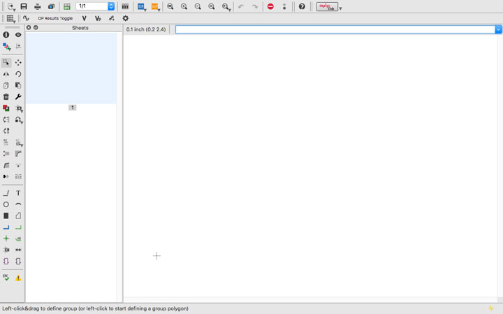
I create new Schematic.
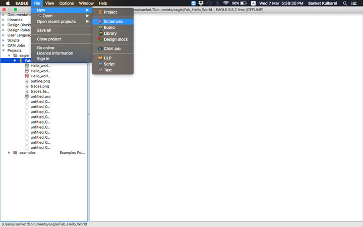
New Schematic.
I wrote 'add' in the address bar.

and opened the 'Library Manager'
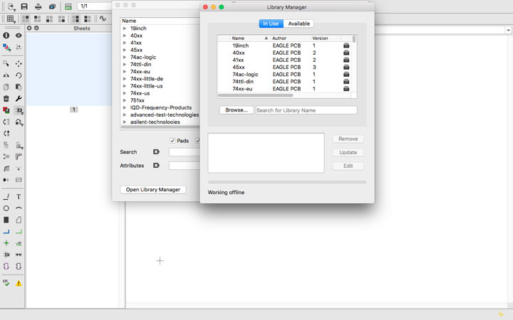
after that i added the downloaded 'fab.lbr' file.
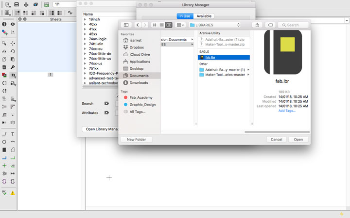
I got the all components.
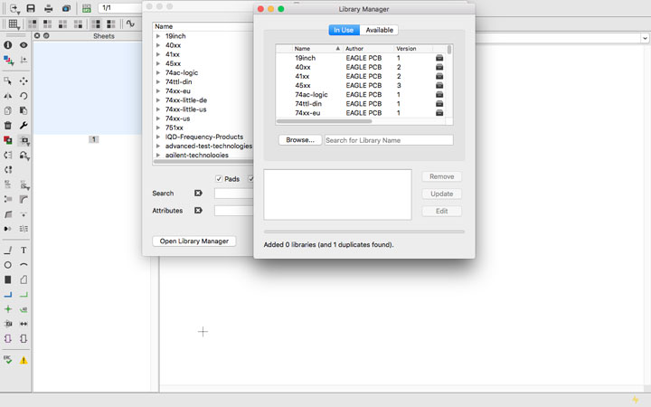
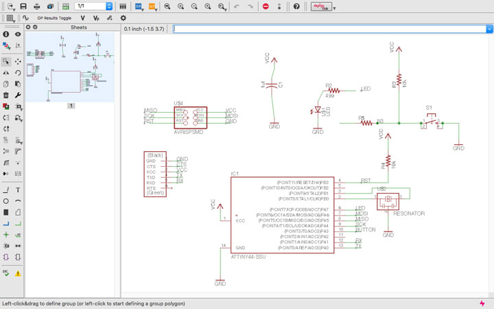
I took the following components For the 'Hello world board' from Fab Library:
1.ATTINY44-SSU x 1 - Microcontroller
2.LEDFAB1206 x 1 - LED
3.CAP-US1206FAB x 1 - Capacitor
4.RES-US1206FAB / 49k x 1 - Resistor
5.RES-US1206FAB / 10K x 2 - Resistor
6.FTDI-SMD-HEADER / 1X06SMD x 1 - FTDI header
7.6MM_SWITCH x 1 - Switch
8.RESONATOR - Crystal oscillator
9.AVRISPSMD / 2X03SMD x 1 - Haeder 2X3
and arrenged the Schematic.
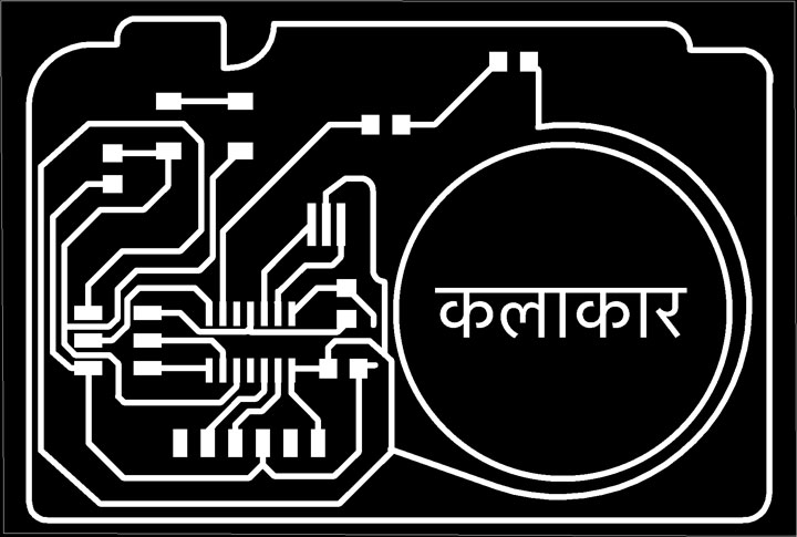
As being photorapher I wanted to make my board as in a camera shape. So I created a vector file in illustrator.
Kalakar stands for artist.
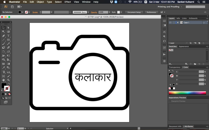
I saved that file as bitmap.
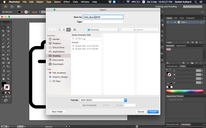
After saving it I ran 'run import-bmp' command.
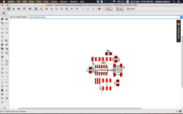
And opened the 'BMP' file.
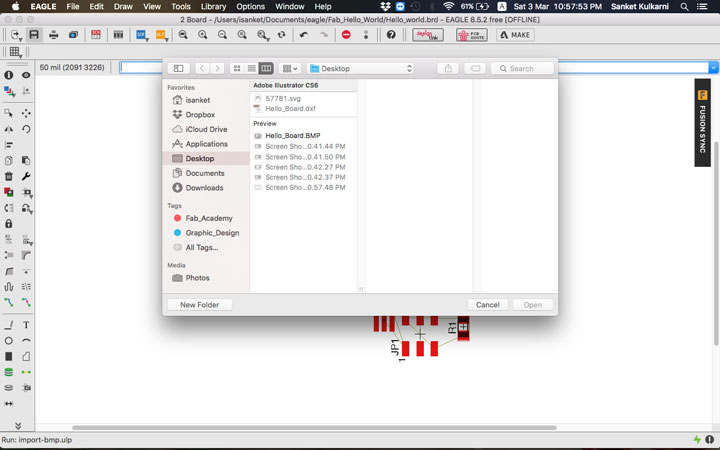
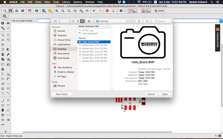
After importing the file a wondow opened. I read all the details and clicked on okay.
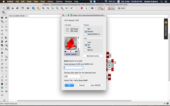
This is how it looked.
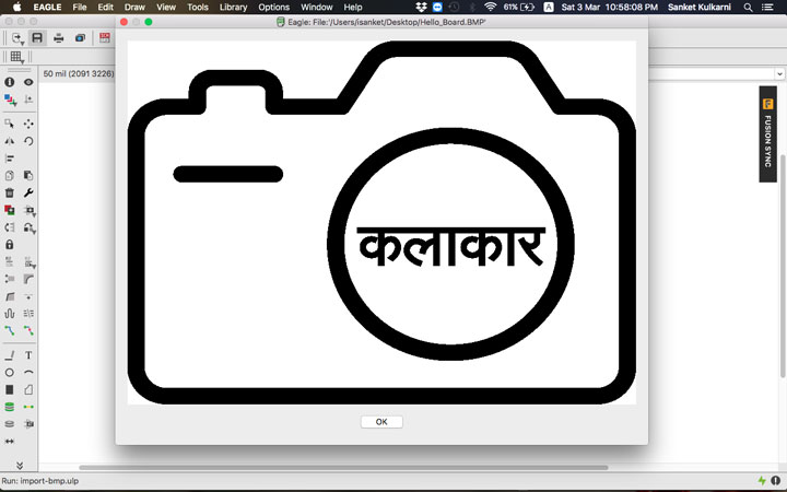
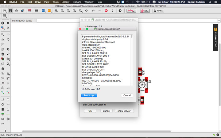
I cliked on the Run.
As I had to arrenged the placement of the components manually according to my design. I deleted the button line in the design which I have imported from illustrator. I joind all the path by using line tool. In this I wanted to cut the shape of the camera, but the outer line width was too thick for the modela. So again I had to make some changes in eagle. in that I eliminated few lines.
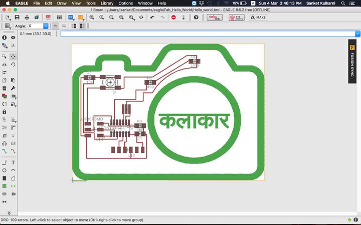
I saved the outline and traces files as a .png format.
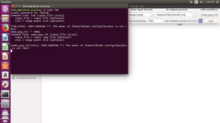
I started the Fab modul.
and loaded my file.
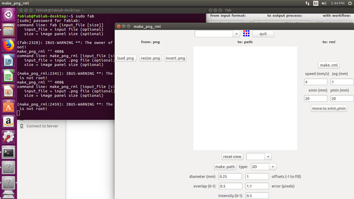
I set the ofset of 4. and clicked on make path.
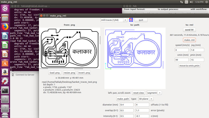
This is how it looked.
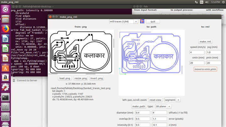
Then placed my pcb on the bed of modela. and again I forgot to take photographs while setting up the tool and setting up the gravity.
After setting up the gravity clicked on begin milling.
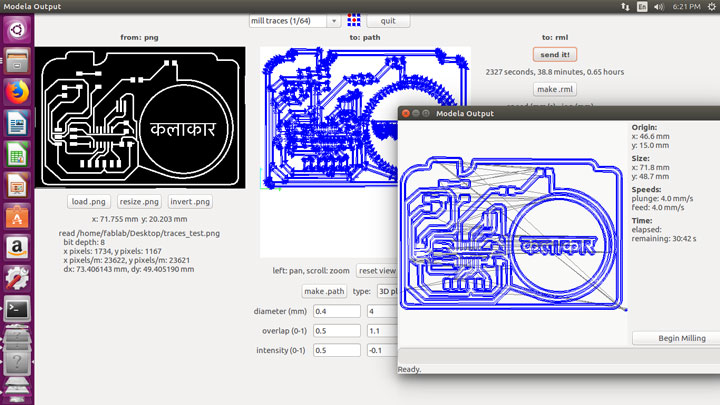
and it started milling the board.
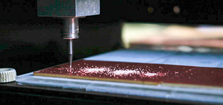
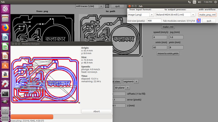
At the first place the endmill did not do his job properly. The machine was cutting the tracks. So I have to do this again.
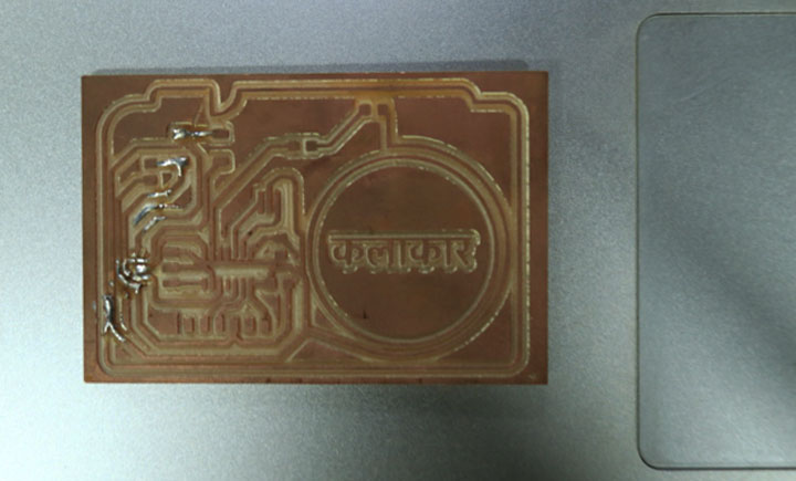
I milled the board again. this time modela did his job nicely. After milling the board I changed the endmill from 1/64 to 1/32. Again I set the gravity and started cutting. The machine took that outer line twice and it started cutting. as I saw it I stoped the machine and took out the board. I wanted to use the board, I cuted the board manually. then I soldered the components.
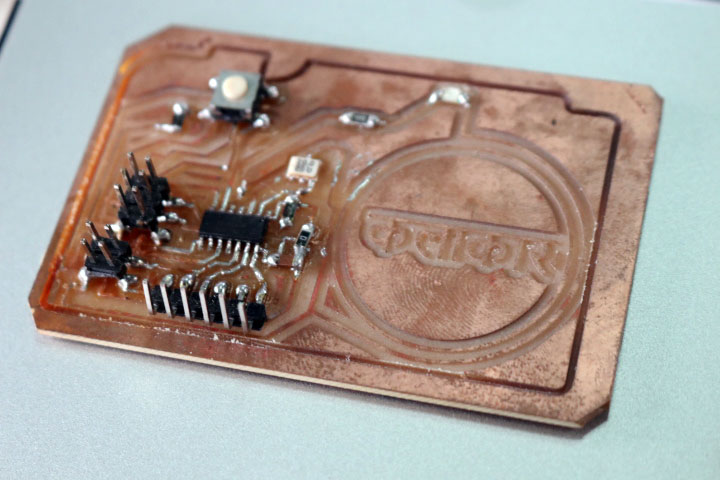
As I took the board for programming it did not respond me. So as per my instructor's guidence I checked the soldering of the board. but that also did not worked. then I checked my boad diagram and schematic, so I found that there are few problems with my board. The schematic is wrong. the orientation of the button was wrongly placed. Then instead of changing path and board I found that making new board will be easier than de-bugging this. de-bugging and re-arranging the tracks would have taken so much time. (I wanted to finish the assignment!).
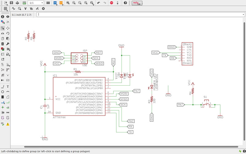
This time I made the schematic carefully and checked with my instructor. here is the new schematic and board design of my hello board. As you can see in the schenatic I have puted the 0k resisters to use as a jumper.
The Design Rules:
as per Google, Physical verification is a process whereby an integrated circuit layout (IC layout) design is checked via EDA software tools to see if it meets certain criteria. Verification involves design rule check (DRC), electrical rule check (ERC).
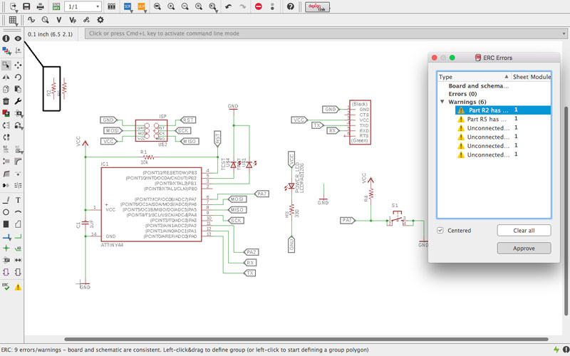
To do this ERC and DRC tests I opend up the schematic and went to tools. and clicked on ERC. a small window came and I saw where exactly problme was.
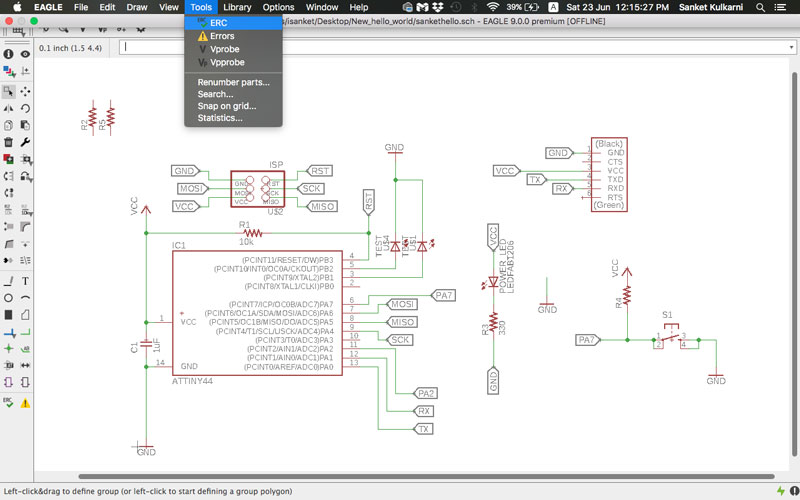
So as you can see there are few worning as I opend the ERC.
I saw the warning. and clicked on approved.
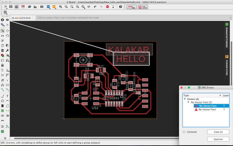
The same way I did the DRC test. I opend up the baord. went to tools and clicked on DRC. again a window poped up. to begun the test I clicke on check. and this time a small window came up. As you can see there are only 2 errors of vector. So I wanted that name on my baord. I clicked on approve.
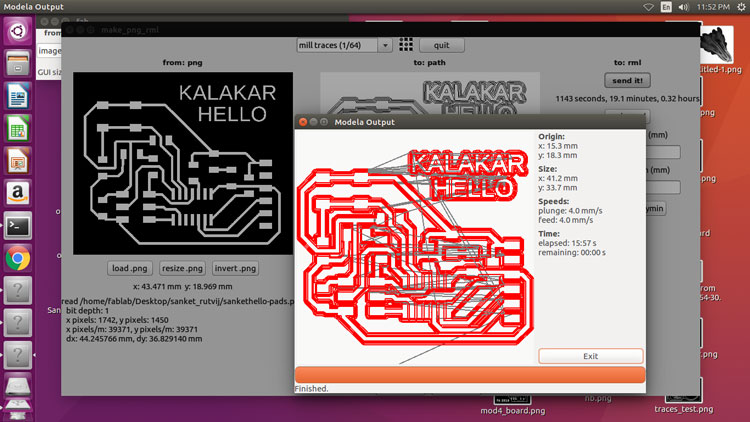
I saved the file in .png format. and imported in fab modules to mill the board.
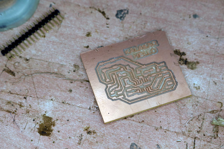
Here is the milled board.
I took the components and started soldering.
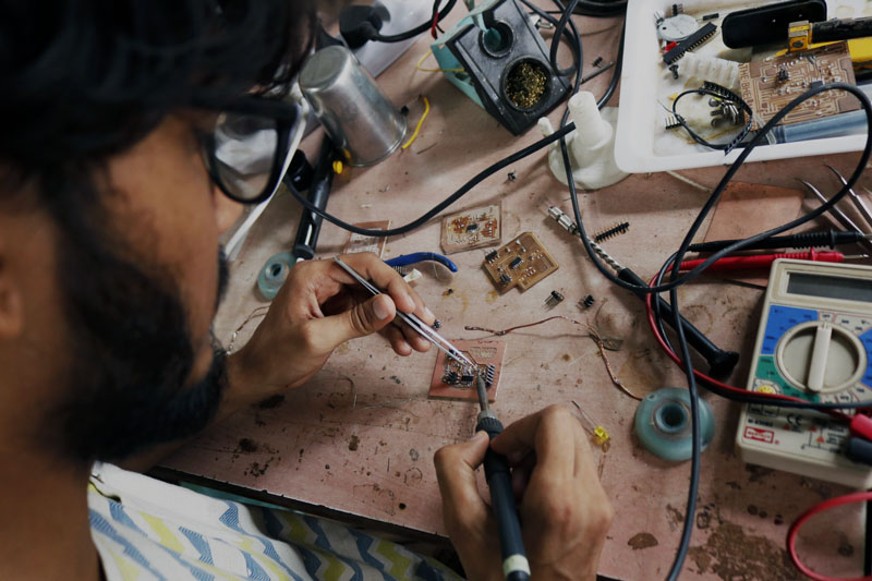
Here is the picture of the soldered board.
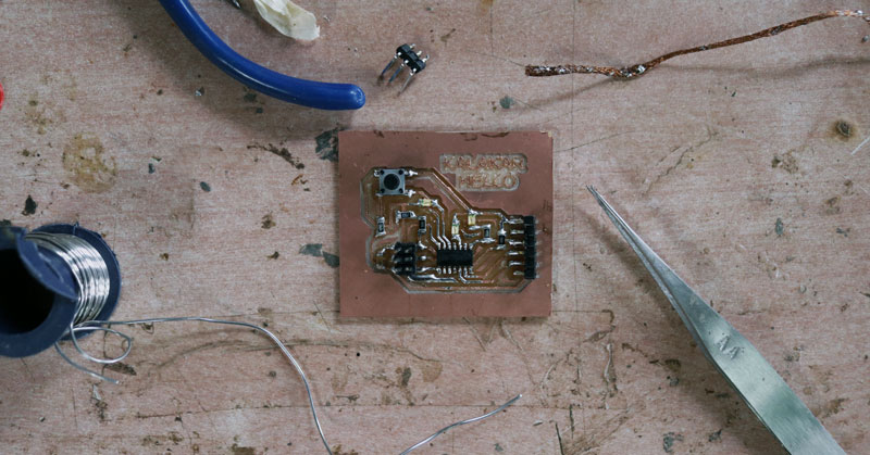
well I heard that A person who naver made a mistake, never tried anything new.
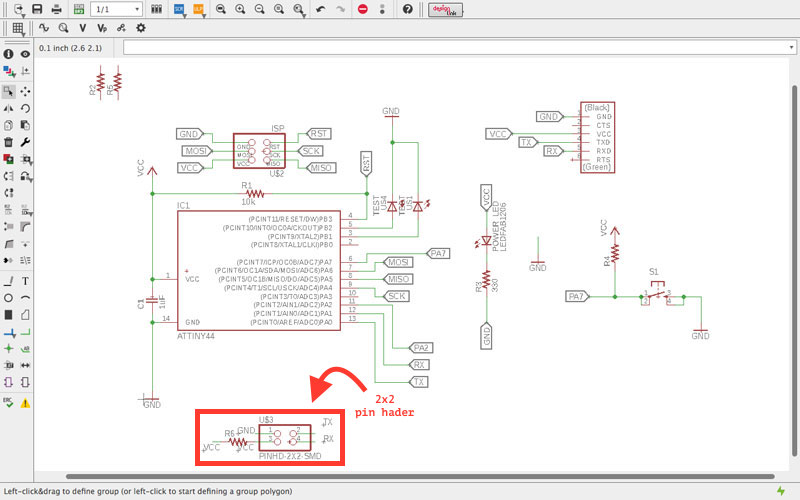
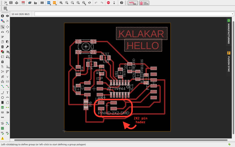
in my case that happens all the time. this time I forgot to add a 2x2 pin header.
I wanted to use my hello board in networking assignment as main board. so I added
the 2x2 pin header in schametic for RX and TX, did all the steps I have done erlier
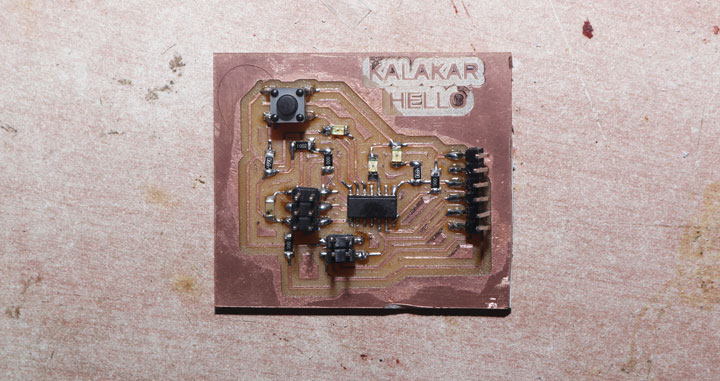
with ERC and DRC and milled the board again and soldered it.
This is the new schematic and board of my hello board.
Here it is the new soldered board!!
Learning Outcomes:
In this assignment I got the chance to practice my electronics and soldering skills. I also learnt more about egale. I successfully imported a vector in eagle. I enjoyed. another part is I did lot of mistakes while doing this assignment and I learnt that I you fail at the middle you definatly will reach at the end just do not give up.You can Download the .png files from here.