This week we had group assignment, this may cause the same image to appear on pages of multiple students
This week were tasked with:
1: Group assignment:
use the test equipment in your lab to observe the operation of a microcontroller circuit board
2: Individual assignment:
Redraw the echo hello-world board
add (at least) a button and LED (with current limiting resistor)
check the design rules, make it, test it, simulate its working and render it
Being from mechanical background I have little no idea about the various components. The main objective of this assignment was to get familiar with the the various electronics design softwares, and the flow path of designing the actual circuits that will be used in future assignments. We had to redesign/redraw Neils' FTDI board and add a LED and a button. It sounds simple, but I knew it will take lots of study to understand where to put them.
Everyone in Vigyan Ashram uses Eagle exclusively, I wanted to try something different. For previous assignments, I downloaded the softwares. Given the limited connectivity I don't think it is recommended. This time rather than downloading just to test and then deleting the disliked softwares, I decided to watch tutorials on youtube about the softwares and then decide which to download.
I had made a small list already.
Altium
Eagle
Kicad
Altium
Just searching for altium, gave me a list of tutorials, the one I recommend and watched is on the channel: GabeCohn. His videos were short and to the point.
There are a few things that I liked about Altium. The userinterface is beautiful. It has interfaces with with SOLIDWORKS. The software feels industry grade.
A demo from the Altium website
The main problem which I think is that there are no already available libraries for altium. Being a newbie, It might be quite a learning curve for me. it also may mess up my board. Also, there is no free edition available. The trial is also limited for 15days. And it is ~4GB in size. Hence I decided against it.
Among the various youtube videos i watched for altium, I recommend this playlist
The guy covers almost everything
KiCad
The next was Kicad, KiCad is an open source software suite for Electronic Design Automation (EDA). The programs handle Schematic Capture, and PCB Layout with Gerber output. The suite runs on Windows, Linux and macOS and is licensed under GNU GPL v3. Kicad has a very strong documentation support. The member community is quite active. Being open source, you can support many OS and distributions, Ki-cad currently supports, 10 systems. If you want you can compile for your OS/distribution. There are lots of member submitted tutorials for Ki-cad, I prefer textual tutorials by Ki-cad itself. Much of the user submitted tutorials are old (circa. 2013) and might not work well with the new, 4.07 version of Ki-cad. The user interface feels dated and needs a overhaul imo. I love open source projects so can look past it. Basic workflow of kicad is-
Create a project.
Create a schematic with 'eeschema'.
Assign footprints to symbols and generate the netlist.
Create a board with 'pcbnew', importing the netlist from 'eeschema'.
Test the board using the 'Design Rule Check'.
Generate production files.
After watching a few videos on youtube, Ki-cad feels less powerful, more convoluted and tad ugly.
Eagle
The next software I tried was Eagle. I had previously downloaded eagle but never used it.
I could not get the hang of Eagle UI. Some of my colleagues were using commands some were using icons, also the UI was very frustrating. You have to press the Esc key every now and then. In my past experience, I have worked on well designed CAd tools like SOLIDWORKS, CATIA. This was almost opposite. Many times I was terribly confused. I spent a good amount of time just clicking through the various buttons. For eagle, I went through the tutorials by sparkfun.
How to Install and Setup EAGLE
Using EAGLE: Schematic
Using EAGLE: Board Layout
Designing PCBs: Advanced SMD
Importing Custom Images into Eagle
The Advanced SMD tutorial is quite long and only recommended if you are into it. Importing custom image into eagle is a good read, but not really necessary, I didn't use it anyways.
The first 3, Setup, Schematic, Board are a must. The tutorials are old (almost 4yr) Some menus/icons have changed
Going through the tutorials, eagle is quite a powerful program. It loves the Esc key for some reason. Also eagle felt more easy to use than ki-cad (maybe because I had it downloaded). I decided to do my PCB in eagle itself.
A demo from eagle website
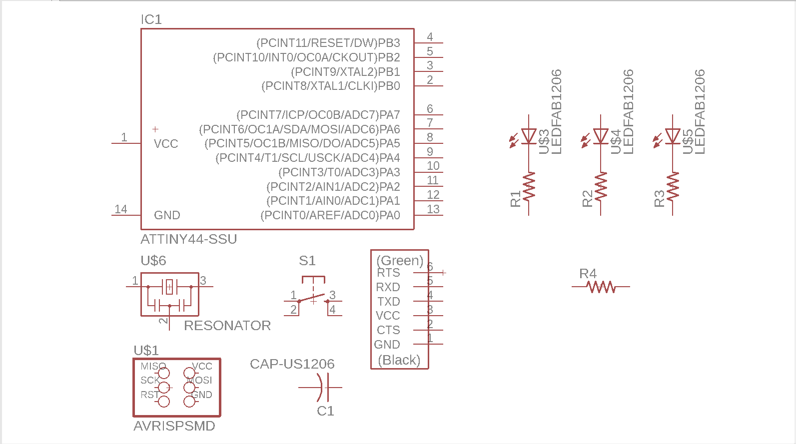
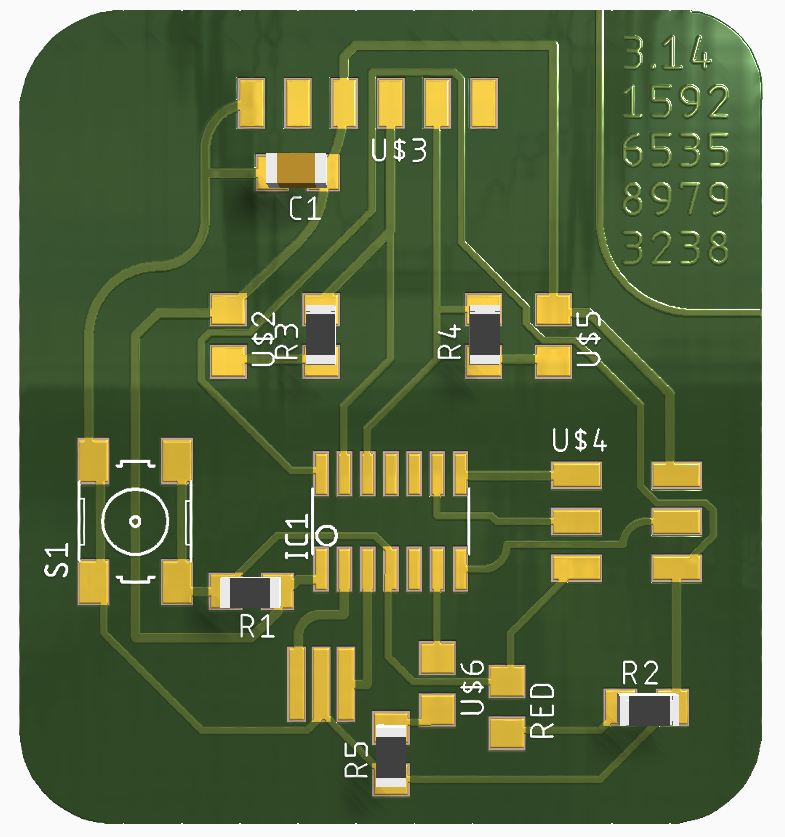
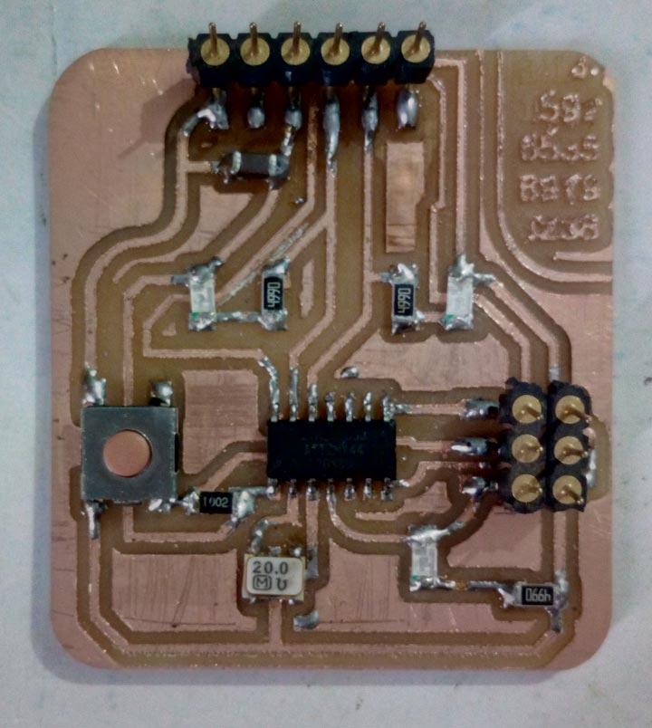
For this assignment we had to Enhance hello board. While sharing PCB designs it is a common courtesy to share the components list, but Neil hadn't done it. Instead he had posted a pic of the completed board. A closer look revealed that the components of Neils' board are as- Attiny-44, SMD pin header, 20Mhz resonator, capacitor and a resistor (10k).
The task is to add a LED and a button, the LED needs a current limiting resistor. Current Limiting as the name suggests, helps to control and limit the current flowing through the circuit. I used Ohms' law to find the approx value of limiting resistor. V = I*R. Thus to reduce current, simply increase the resistance. For the maximun current supported through 1206 LEDs I went through the datasheet
I think, 10 milliampere is more than enough for any smd led. Therefore, 5v = (0.01ampere)*R. The value of resistance is 500Ohms. It is necessary to have low current through my LEDs specially in my case.(more on this below)
There is one thing I love about modems, routers they blink when data is transfered. It gives a physical stimulus. I like it a lot. Instead of adding LEDs to random ports, I decided to add them somewhere useful. I'm adding them at 3 places.
Tx line
Rx line
Power Led
I was worried that the current coming from the LED would draw lot of current and hence corrupt data on the Tx, Rx lines. Hence the low current flow.
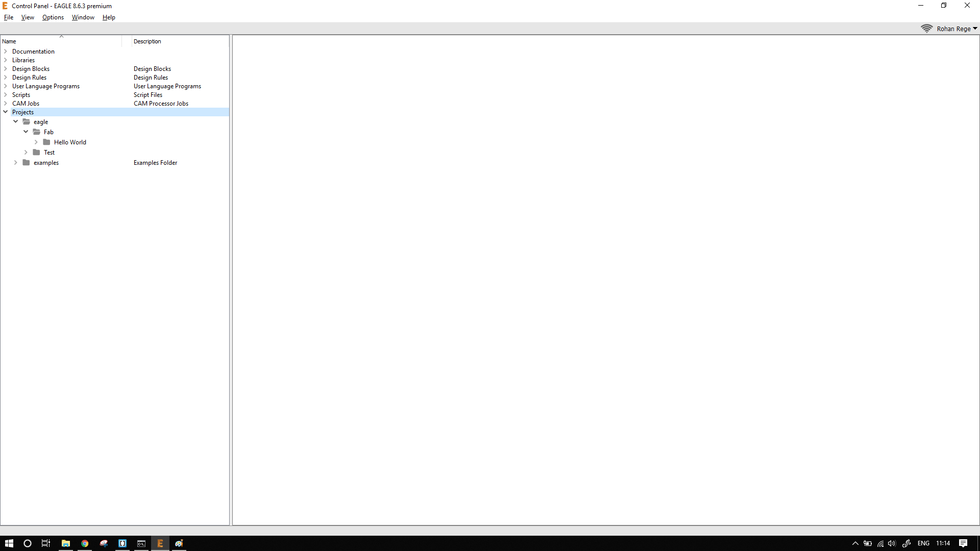
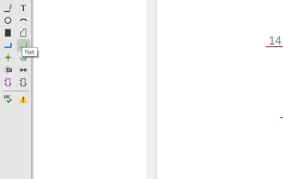
The first thing after opening eagle is the control panel. In the left there are six separate trees.
Libraries – Libraries store parts, which are a combination of schematic symbol and PCB footprint. Libraries usually contain a group of related parts, e.g. the atmel.lbr stores a good amount of Atmel AVR devices, while the 74xx-us.lbr library has just about every TTL 74xx series IC there is.
Design Rules – Design rules are a set of rules your board design must meet before you can send it off to the fab house. In this tree you’ll find DRU files, which are a a pre-defined set of rules.
User Language Programs (ULPs) – ULPs are scripts written in EAGLE’s User Language. They can be used to automate processes like generating bill of materials (bom.ulp), or importing a graphic (import-bmp.ulp).
Scripts – Script files can be used to customize the EAGLE user interface. In one click you can set the color scheme and assign key bindings.
CAM Jobs – CAM jobs can be opened up by the CAM processor to aid in the creation of gerber files.
Projects – This is where each of your projects are organized into a single project folder. Projects will include schematic, board design, and possibly gerber files.
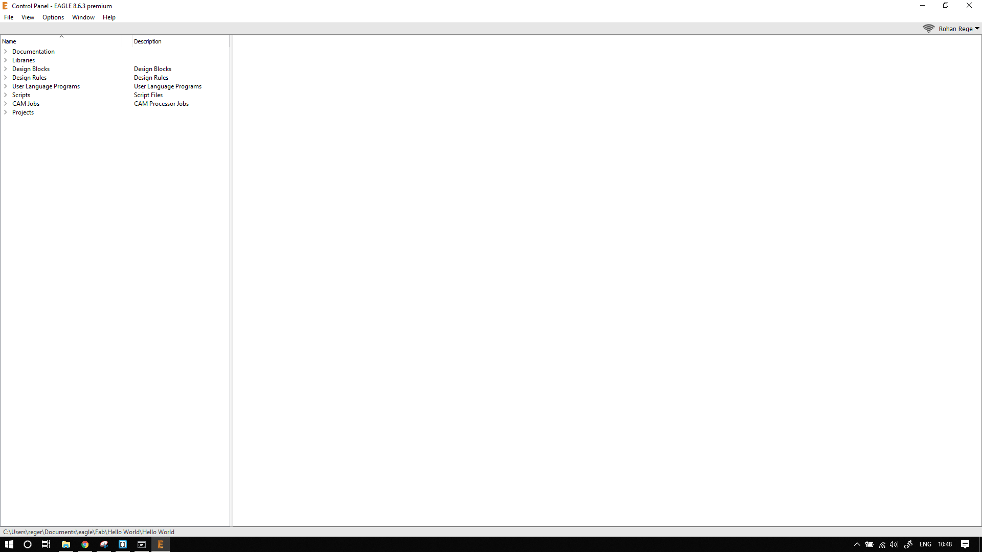
Fab community has already created a library (more on this later) for eagle which contains almost all the common components. To add this library-
Save it to the default Eagle Library folder or add the library folder to the eagle directories
Go to options -> directories -> Libraries
To use the library, click on the "fab" folder in the library tree and select "use all"
(optional) If you want to avoid confusion, select all the other libraries and select "use none"
The user interface can be edited very easily by running scripts. I recommend this script by sparkfun.
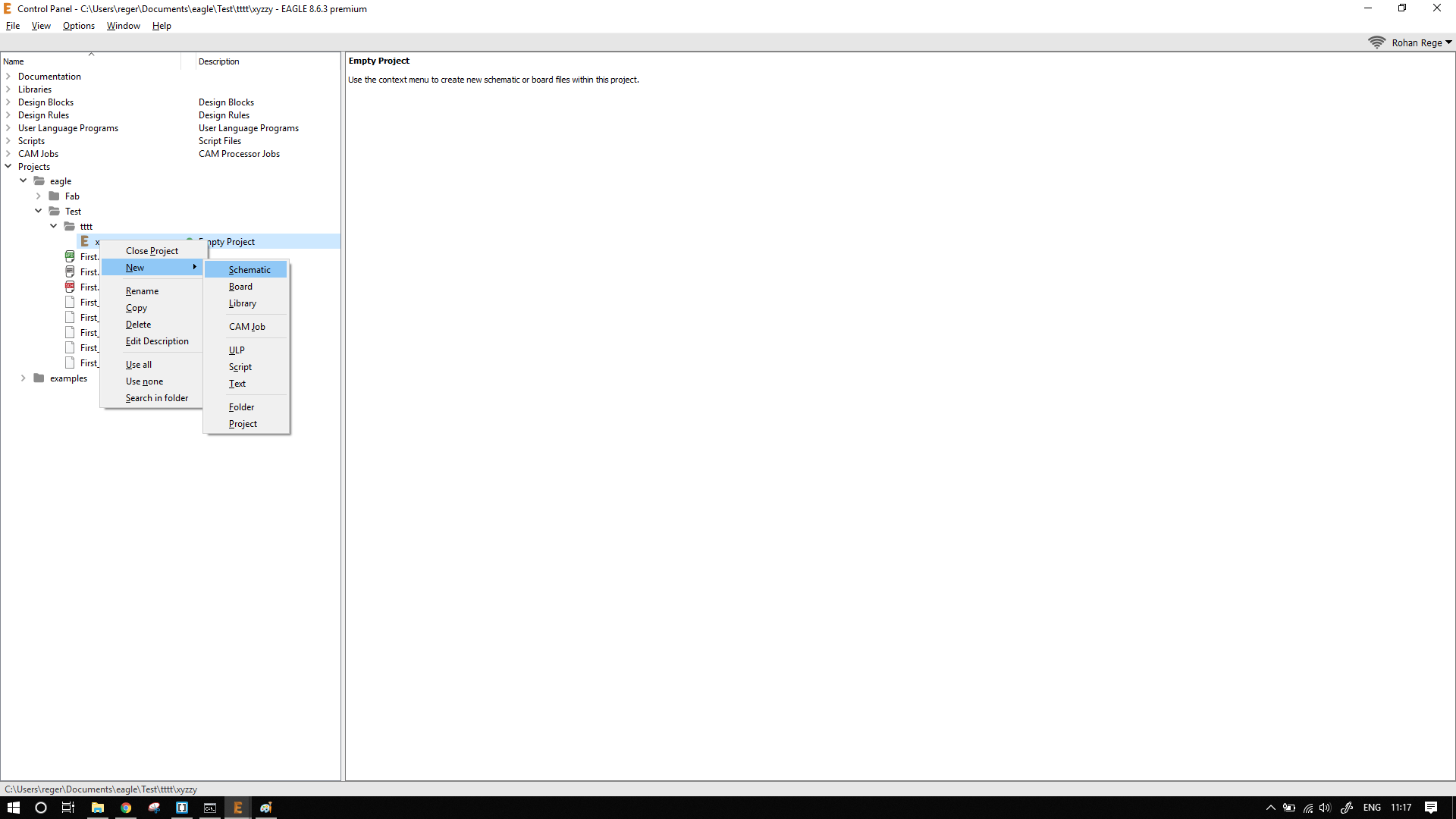
Next create a new folder inside the eagle folder labeled "fab" and then another folder "hello world". This is not really necessary but it reduces the clutter. To make project right click -> new project
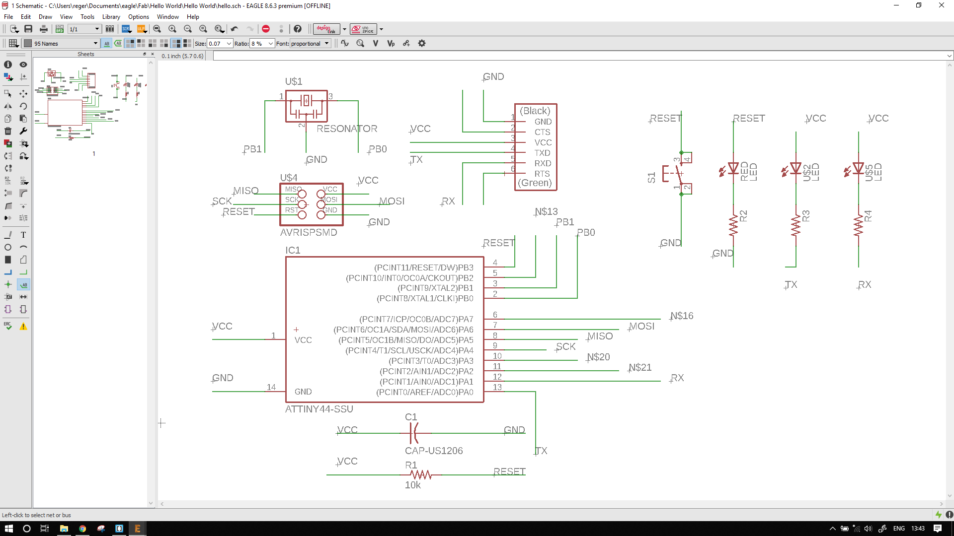
Now select the project and click new Schematic.
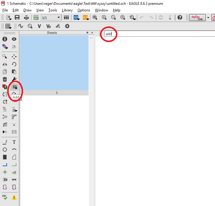
This will open the schematic window. Schematic window is used to draw the circuit diagram. Here we can draw the circuits without worrying about component placement. Generally it is recommended to have the schematic with a sheet border.
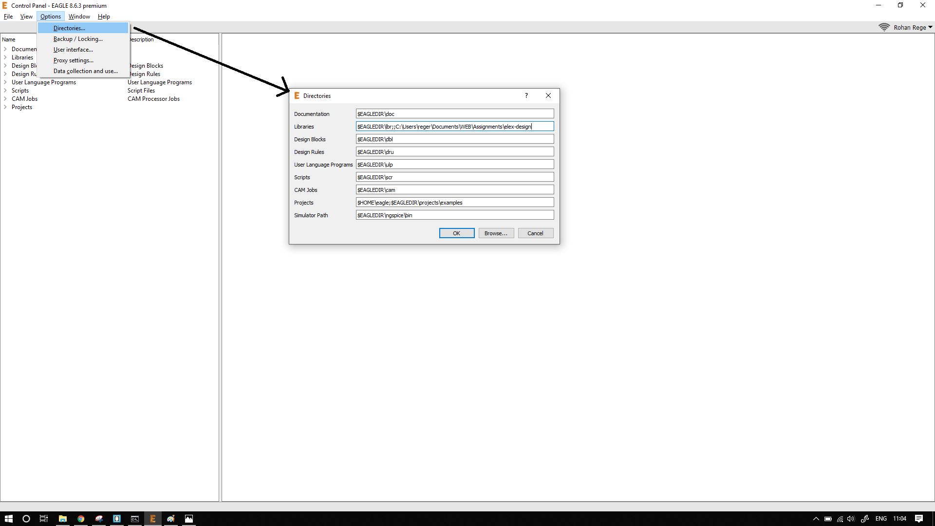
To add components type add in the command window, or click the add button from the toolbar in the left. I prefer the UI.
Then add the add the components required for your board, for me they were-
Neils' hello board components
LEDs (2x green, 1x Red)
Current limiting resistors (3x)
Push to On switch
To join the components together, select the net tool. Start by linking the components together.
This is the easiest method, but it might be confusing, to avoid confusion and for clean routing I recommend making net stubs. Then naming them uniquely, this helps to get a clean route and schematic.
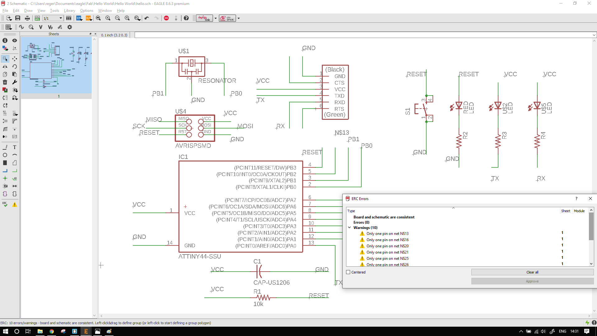
To verify the board is working properly, we need to perform ERC. It is similar to ERC. It will check whether all pins are connected. In my board we have not used all the pins. Hence we might some errors (or warnings).
The next step is to make the board, to make the board click the switch board/schematic button
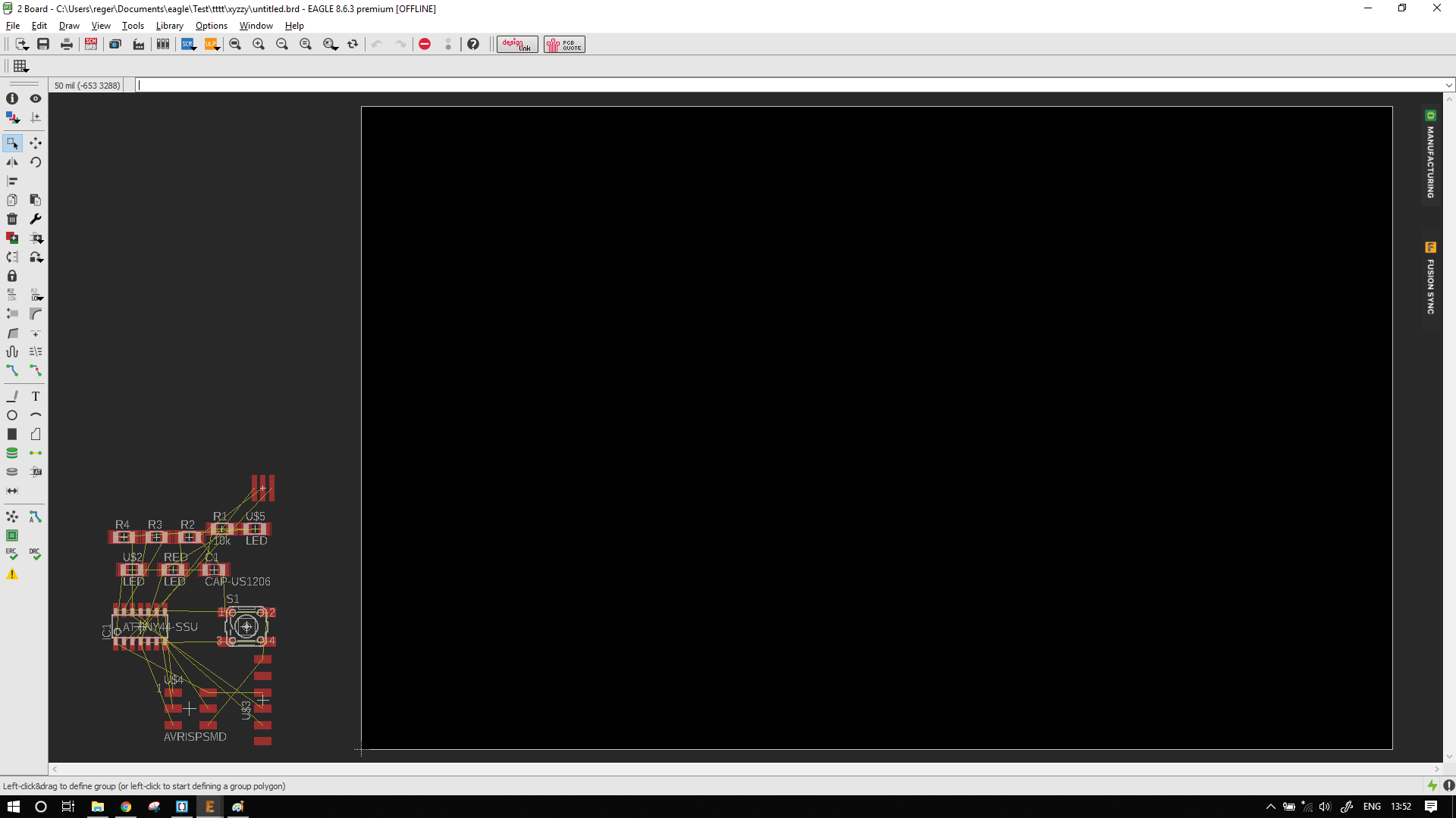
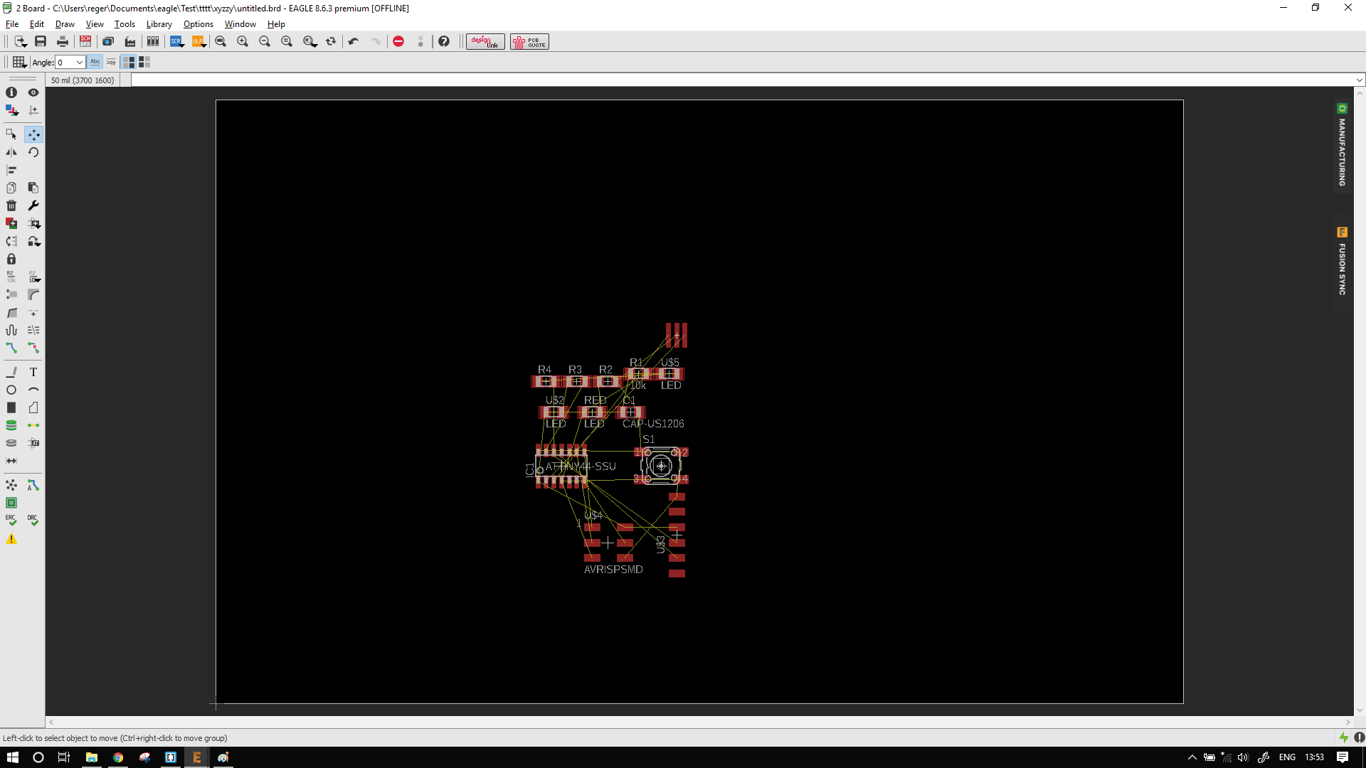
In the board window, move all the components inside the black window.
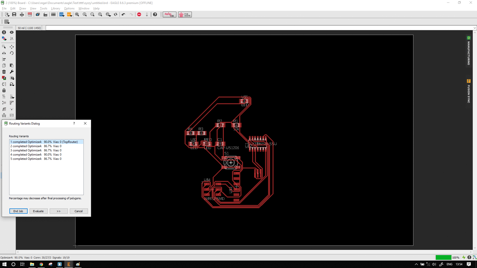
Now use the move tool to place all the components as you like. Eagle has two options to route the board, manual routing and auto routing. It all depends on user preference. I prefer a mix of both.
Arrange all the components the way you like
Perform an auto route
Rip up the the connections you don't like
Manually route the the connections
perform auto route again
Repeat till you are satisfied
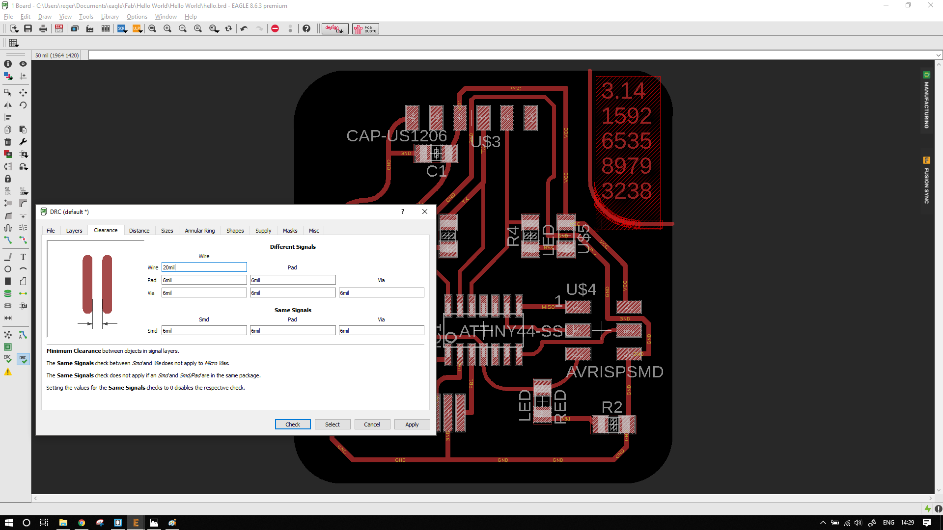
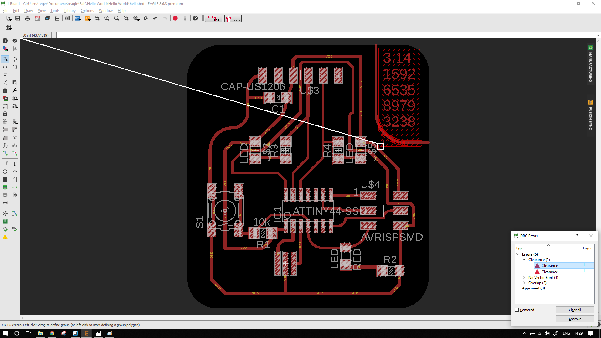
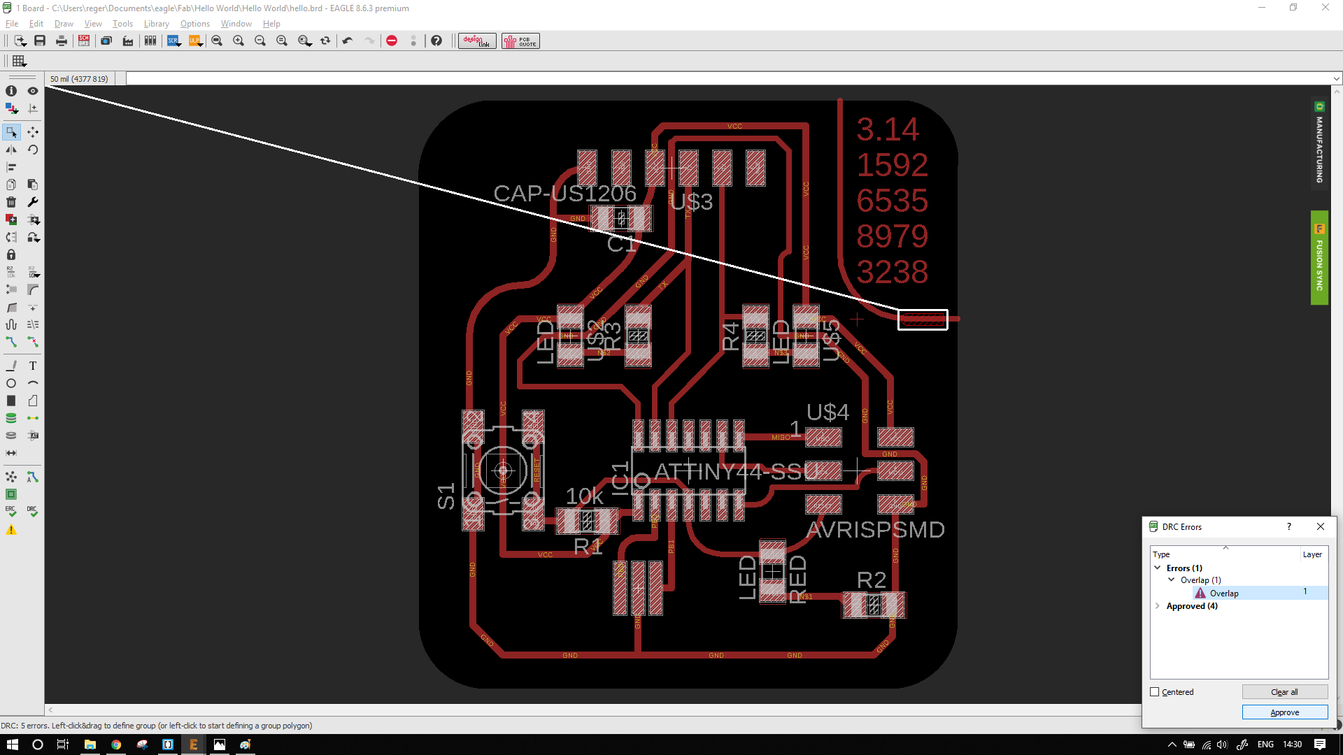
Once everything is done. perform a DRC.
DRC stands for Design Rule Check.
For my case, my route thickness varies from 20mil for almost all connections to 16mil for connections where I felt it would be hard to solder. Drc gave me a few errors but they were due to my personalized decoration on the board. Which I (approved) and chose to ignore.
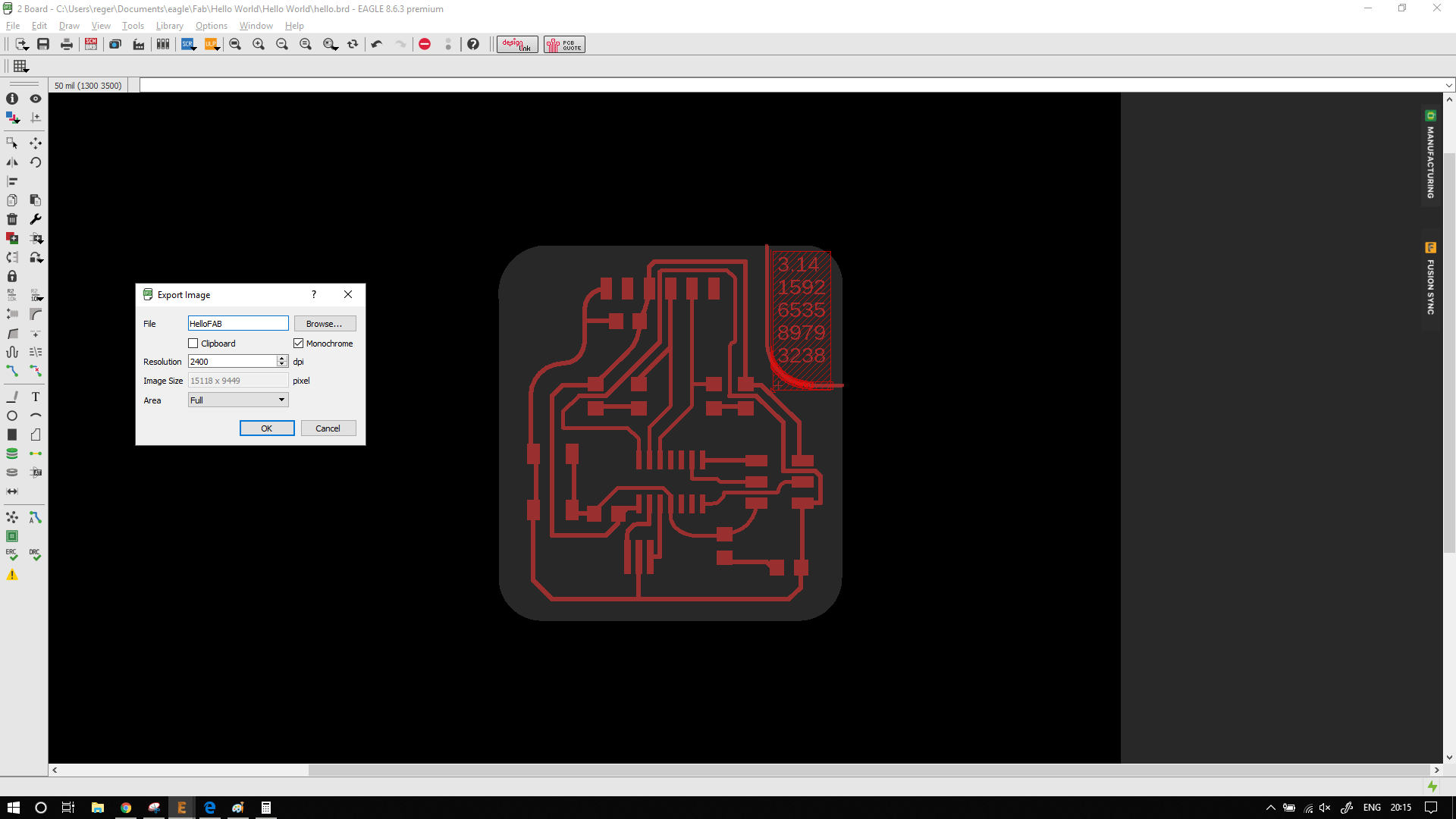
The next step is to draw a border around the circuit. Select the line tool. Trace around the board with approx distance.
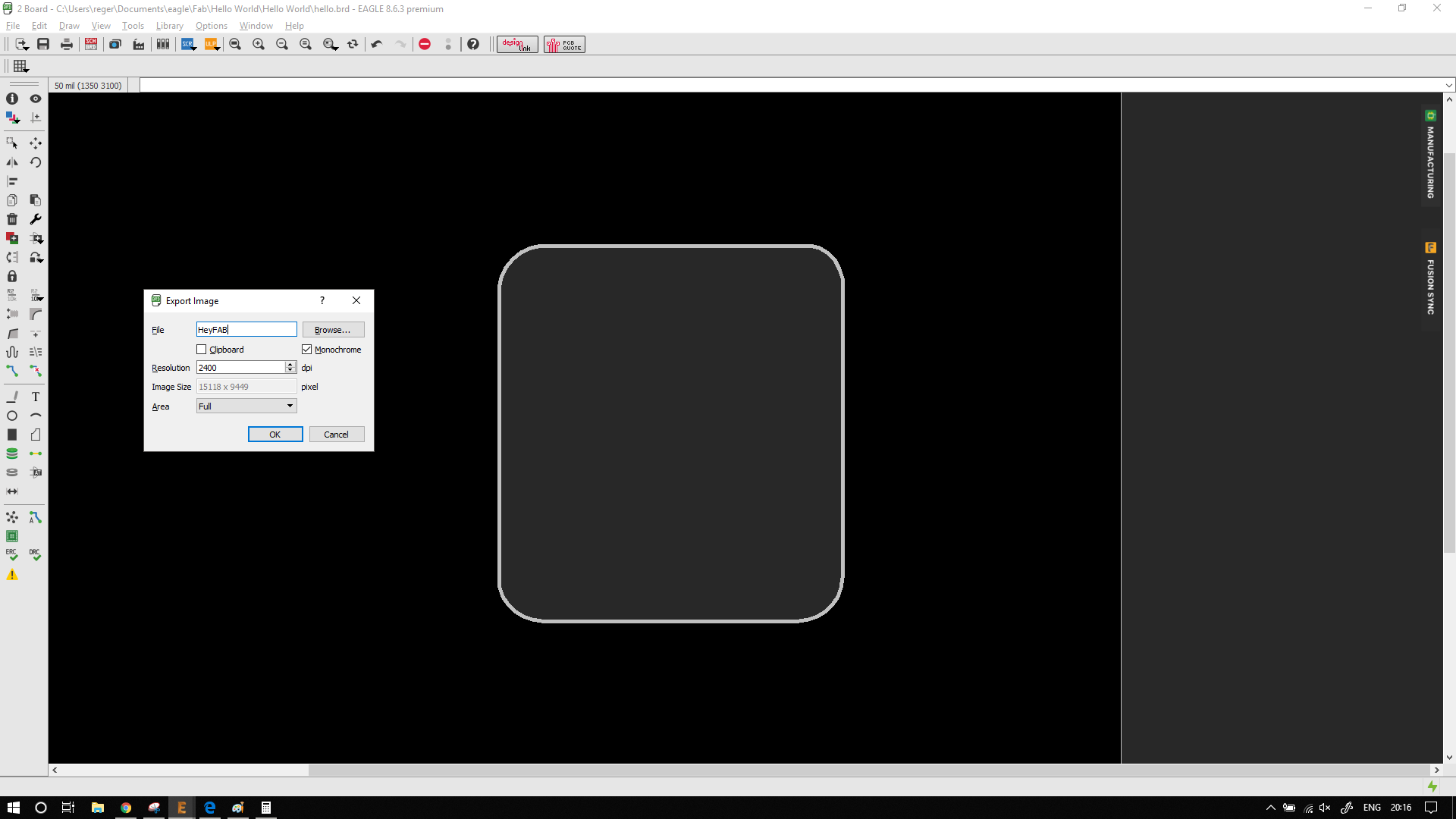
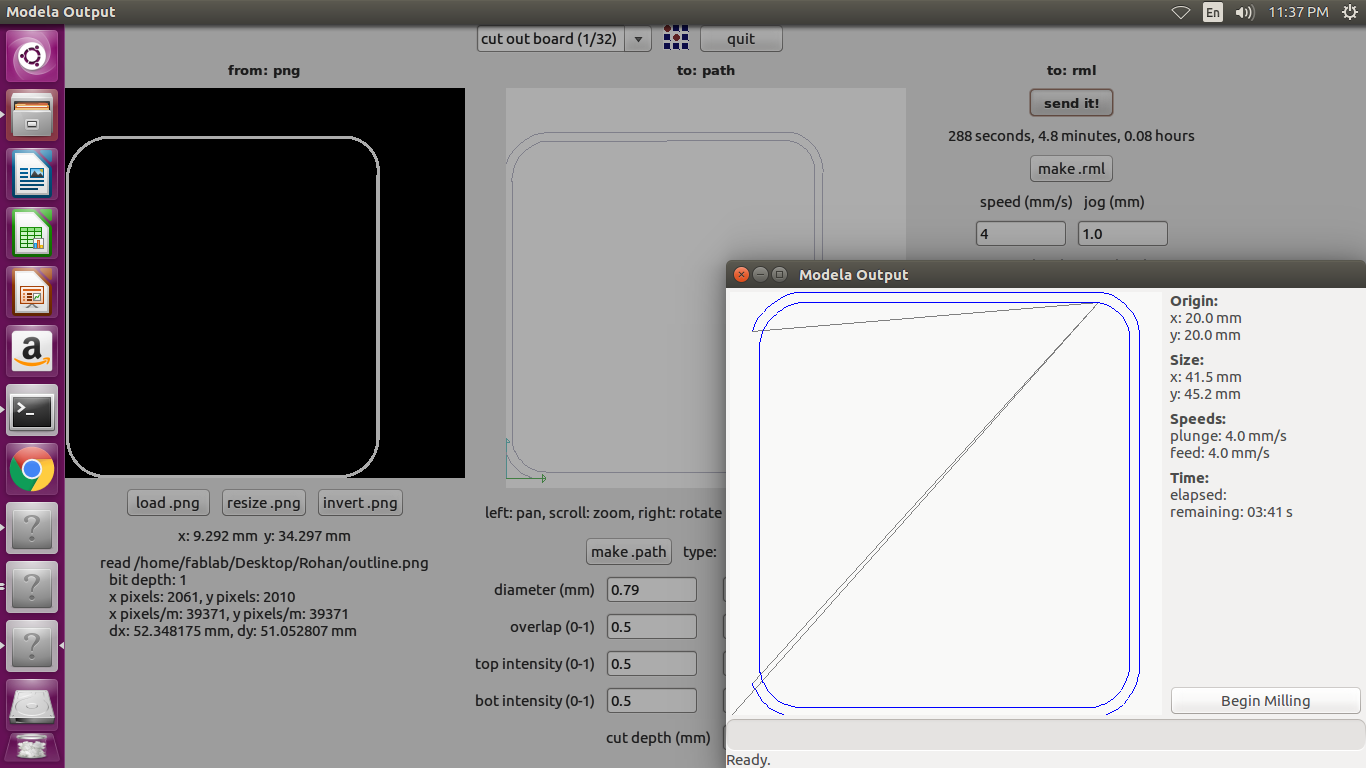
Now export this this as image. The max resolution of modela is 1000dpi also select monochrome option.
Repeat this process for the the internal components also.
You should have 2 images. 1 for 0.4mm milling end which contains traces. The second one with just the outside border for 0.8mm cutout milling end.
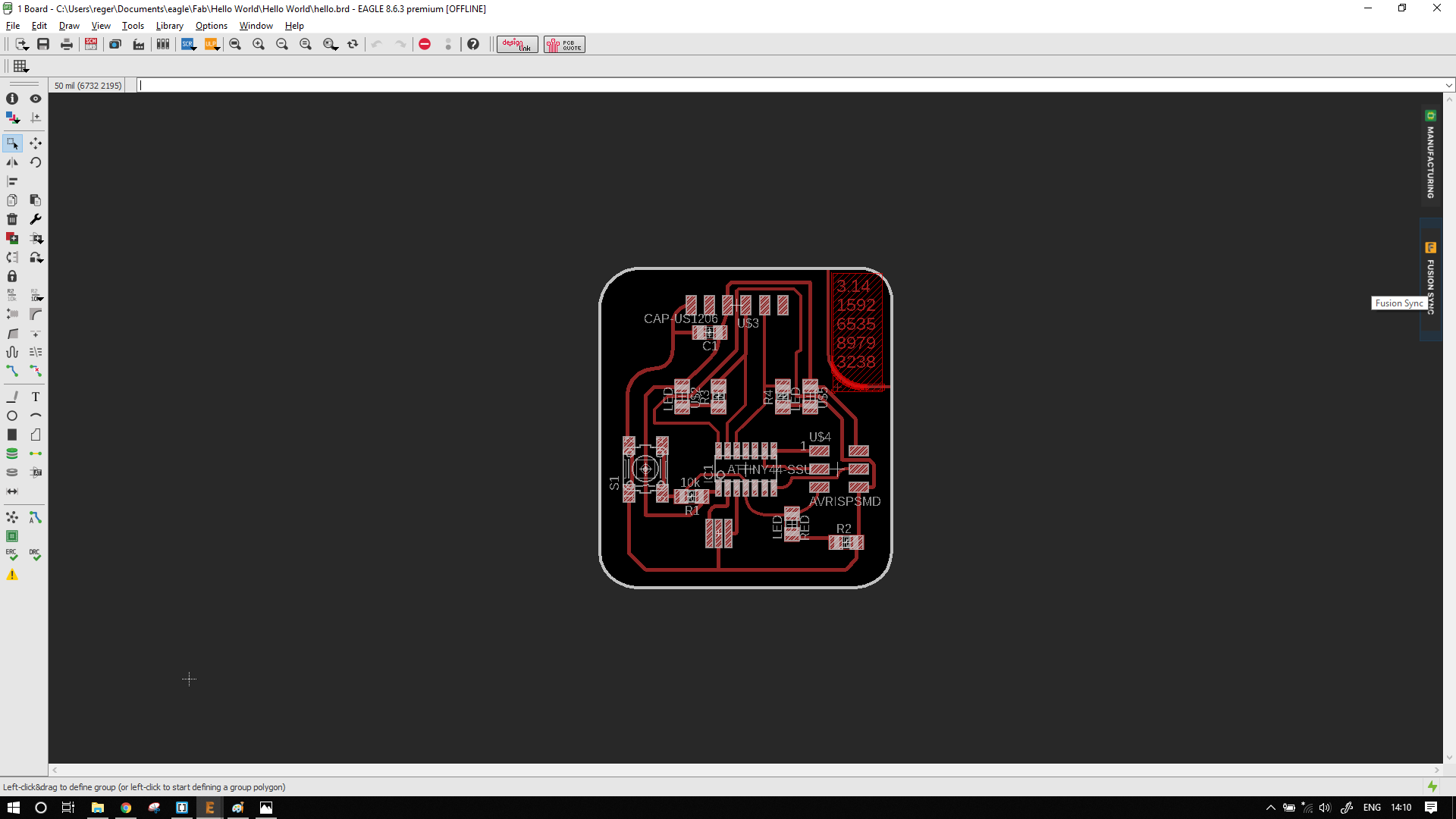
Rendering
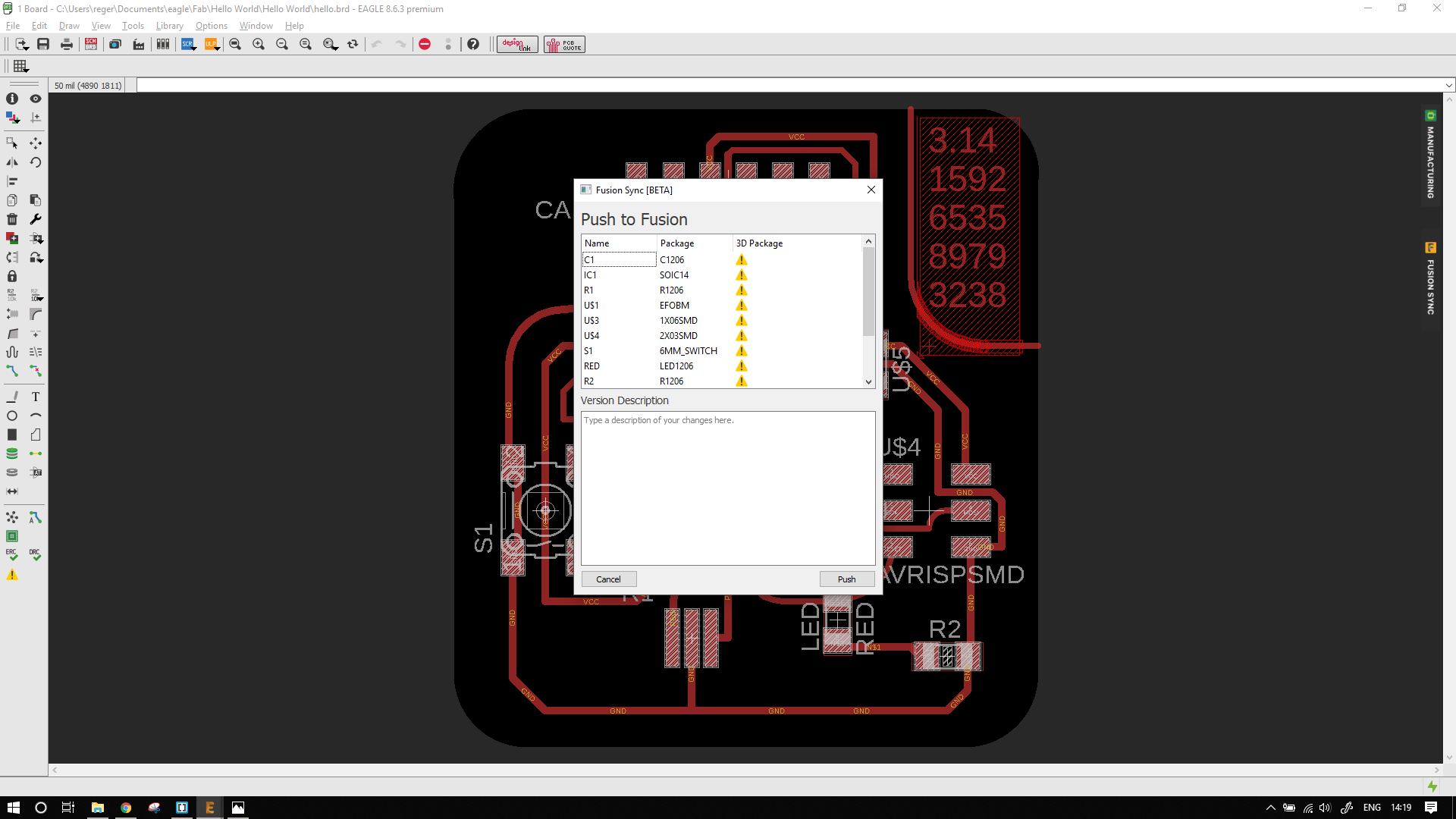
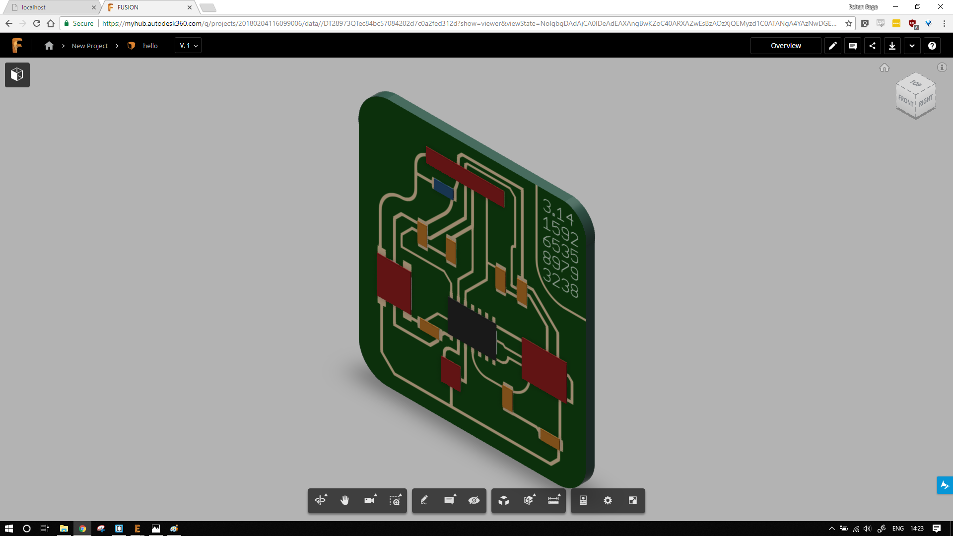
To render the board, I used the inbuilt fusion 360 plugin. In the board screen click on the fusion sync option.
The software is in beta but it works well with small boards.
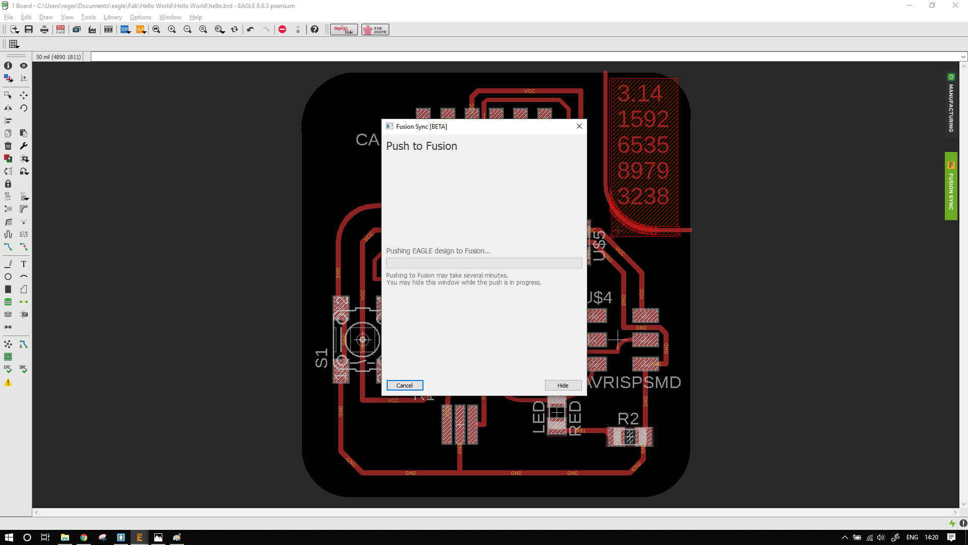
Most of the components I used were from the FAB inventory. They did not have a 3D package. So fusion gave me a warning.
Just ignore the warning for now and push the file to fusion, Fusion will automatically make a 3d package based on the traces specified. This is enough for us.
Now open fusion cloud and search for the file.
After opening it your file should look like above.
This looks good, but I'm not satisfied with just good, I had get something better.
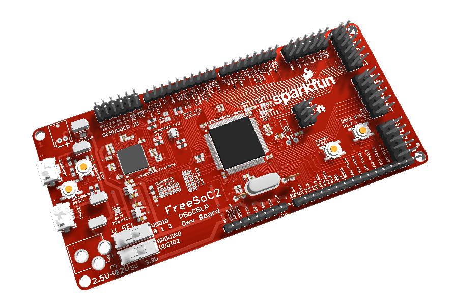
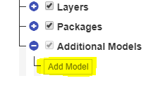
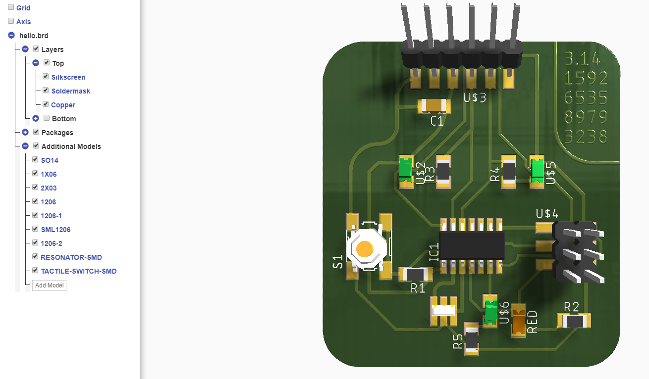
After some searching on the internet. I found 3D BRD Viewer, an online website that will render eagle brd files.
And with demos like the image below, I really liked it
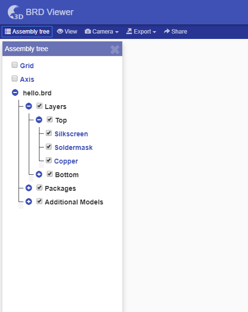
The user interface is really simple.
After loading the board you are presented with a simple assembly tree on the left like so:
Because some components do not have a 3d model, like in fusion, not all the parts are visible.
These need to be added manually,
After adding these components, the is done!
For my hello world board, I've added the following components
SO14 (IC)
1X06 (FTDI header)
2X003 (ISCP)
1206 (LEDs)
Tactile Switch SMD
Resonator SMD
The files can be exported in various formats,
The final rendered file:
In the Vigyan Ashram we have an MDX-20 machine.
We are currently operating it using fab mods.
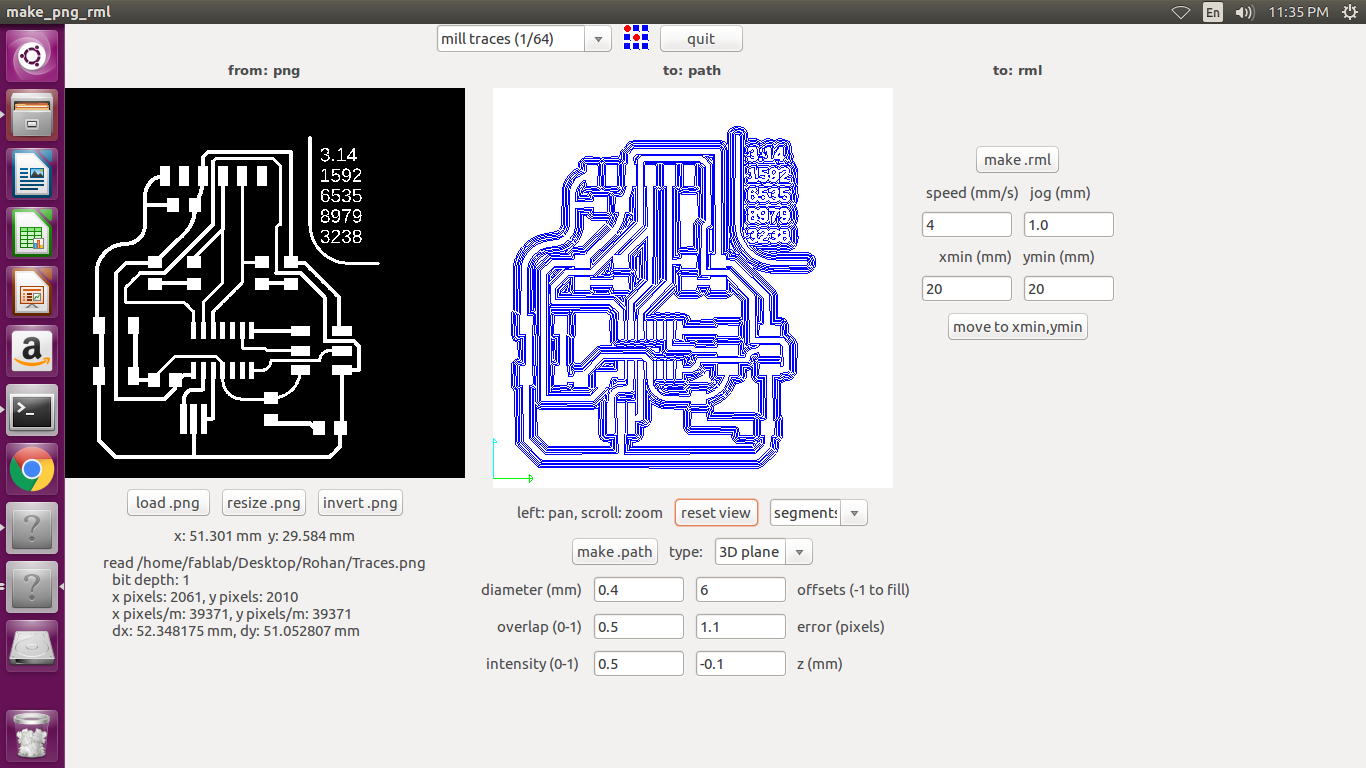
I loaded the exported image in fab mods.
I set the required parameters similar to those during the making the fab isp
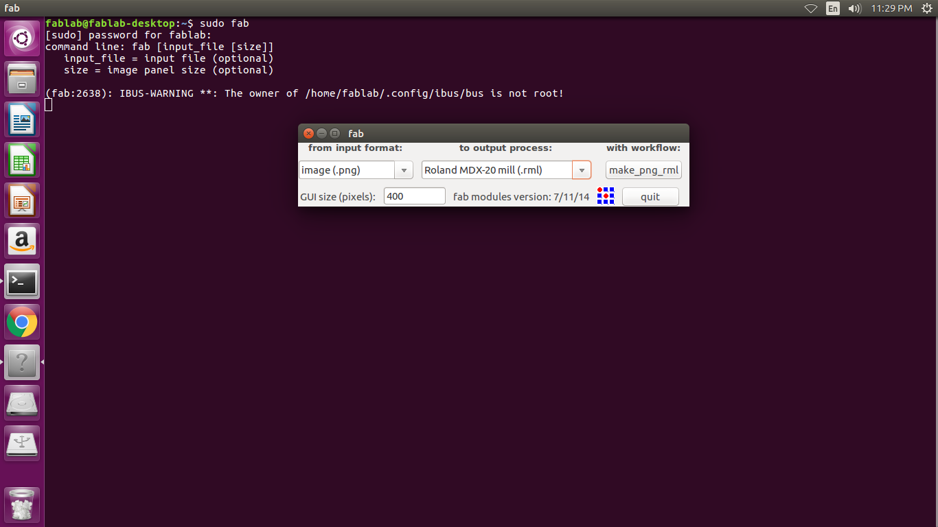
$ sudo fab
Then choose input as .png and output as .rml
Load the .png file and select mill traces and other parameters as per your liking
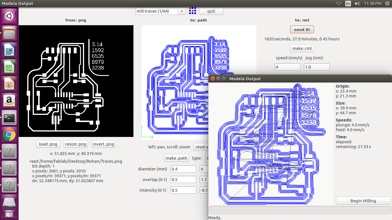
Click make path then make rml and then click send it to begin milling
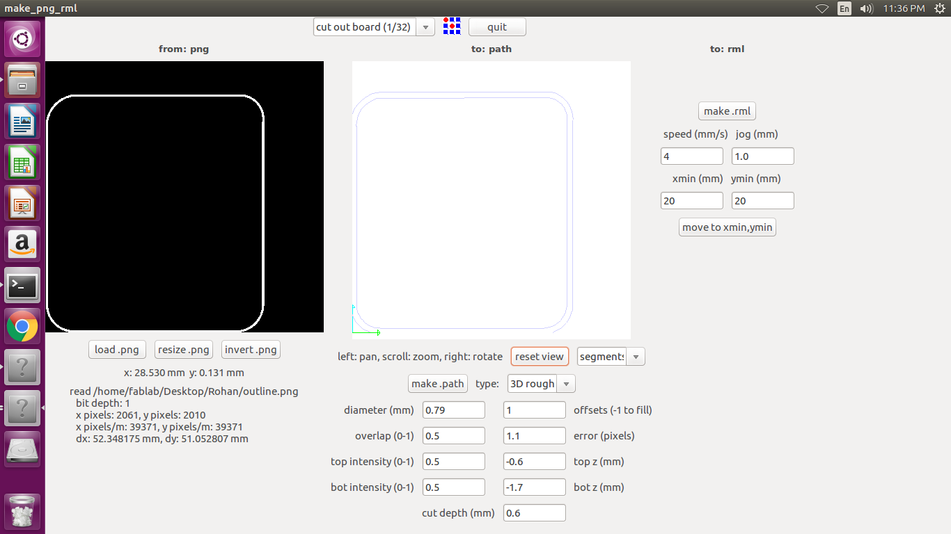
Once done, Load the cutout file and now select the cut out board option
Click begin milling to start the processes, Don't forget to change the bit
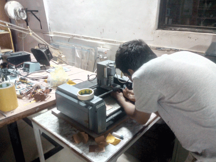
Me working on the MDX-20
The components I need for my board are-
ATtiny44
Push Button 1
Crystal 20Mhz
FTDI header 1X06
ISCP header 2X03
LEDs with current limiting resistors (3X)
capacitor
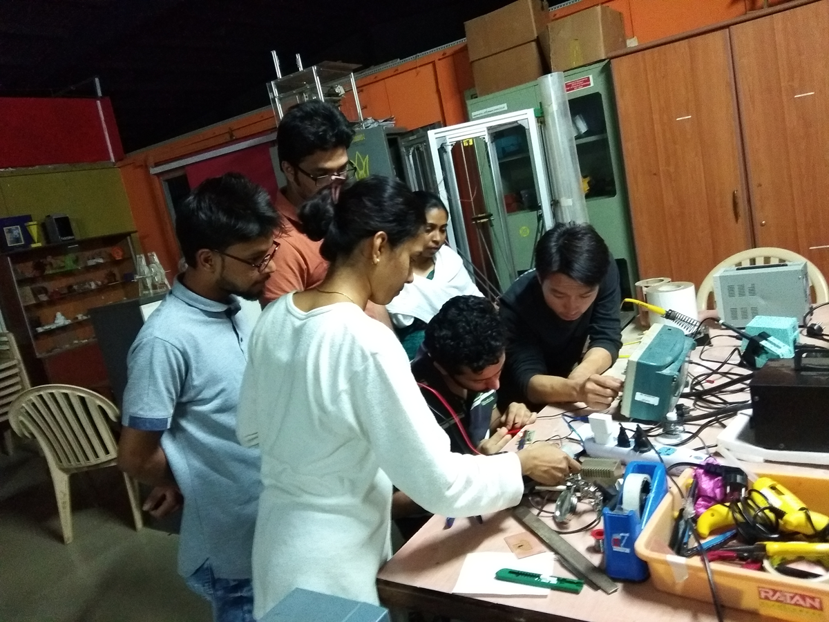
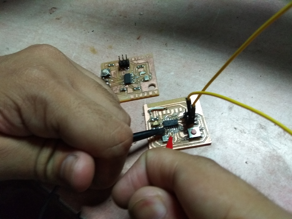
Here is are a few videos of me working on my board.
Once everything was soldered, my board was ready
The tutorial for programming is quite simple as Neil has provided an image here
If we look at the steps closely, we can see that the flow is really is simple:
Step 1: Compile the programme with 'make'
Step 2: Set the fuses of the IC
Step 3: Flash the programme to the IC.
Step 4: Observe the Echo output on python terminal
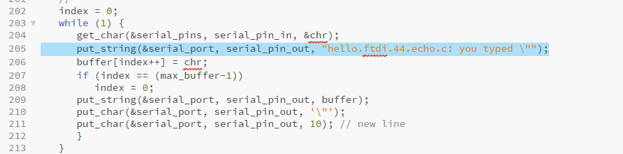
I never run any programme without first seeing what it contains.
Although I dont have much idea about the C, it gives me a basic idea of how the programme was written.
Also gives me a chance to customize the program.
So I opened Neils'program
While, looking through I found that, void main, on line 205, there is a line put_string(&serial_port, serial_pin_out, "hello.ftdi.44.echo.c: you typed \"");
This basically adds the text, "hello.ftdi.44.echo.c: you typed" before echoing your command
I decided to change it to you typed
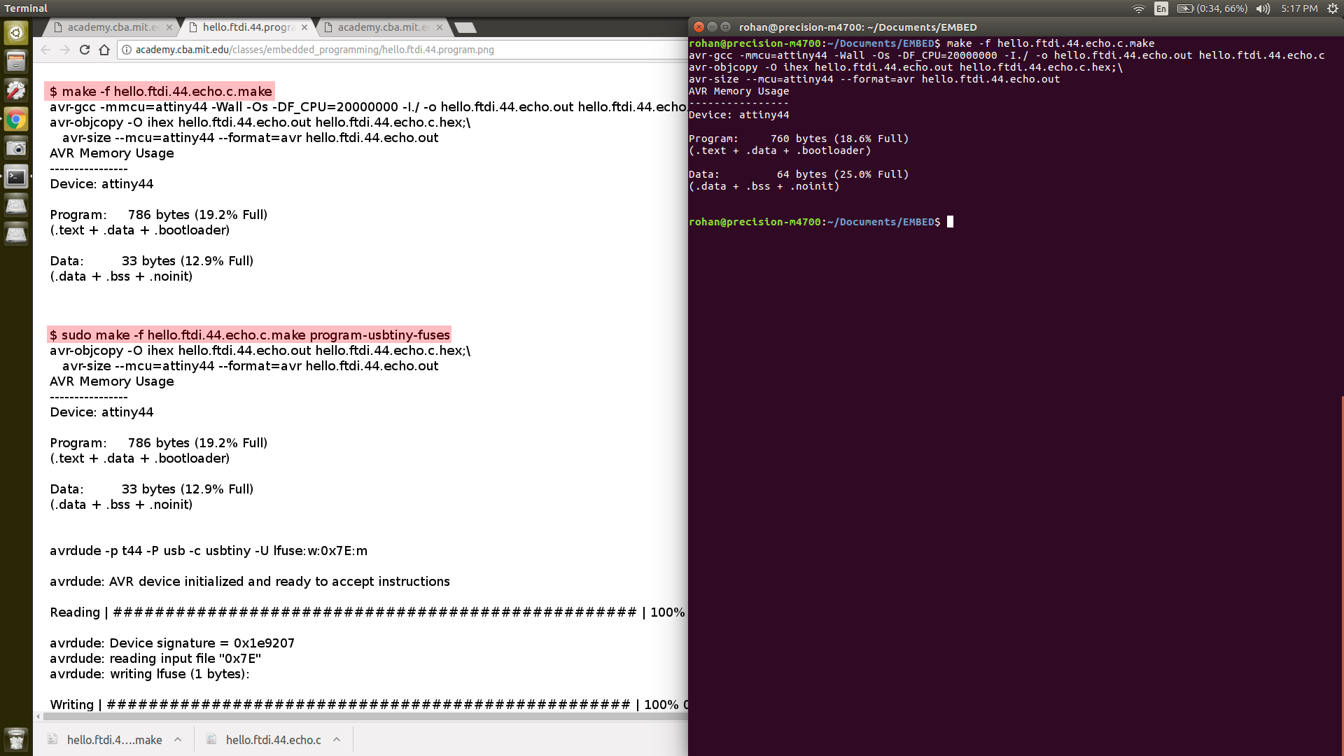
Then I compiled the program as follows:
1: Compiled the programme
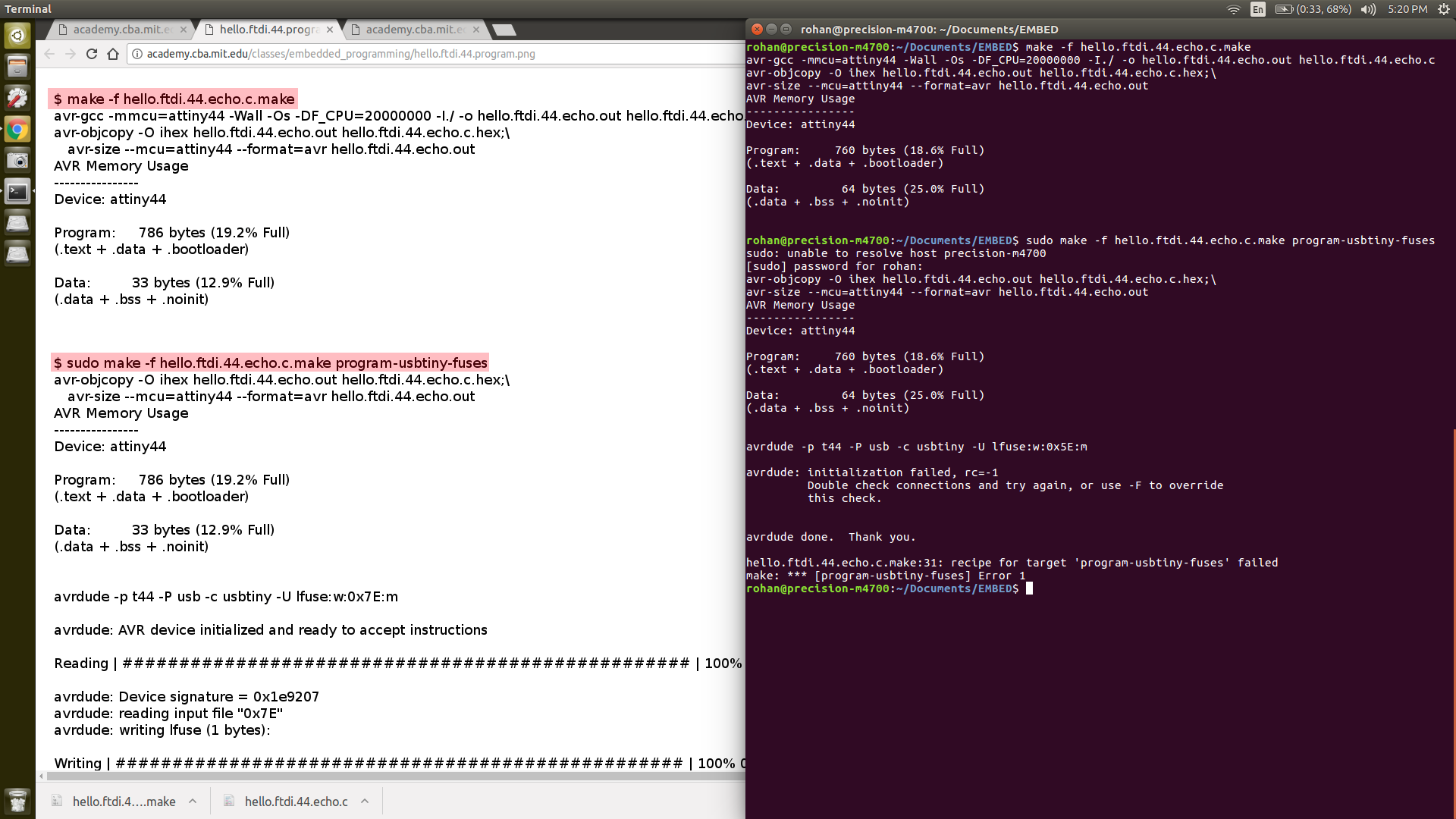
2: Set the Fuses
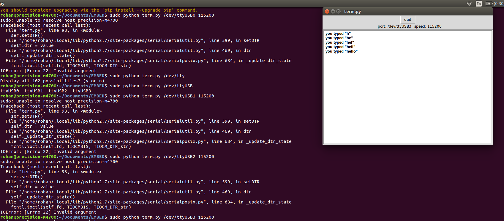
As you can see, I had some error, So i disconnected everything and reconnected everything and after 2 mins it worked.
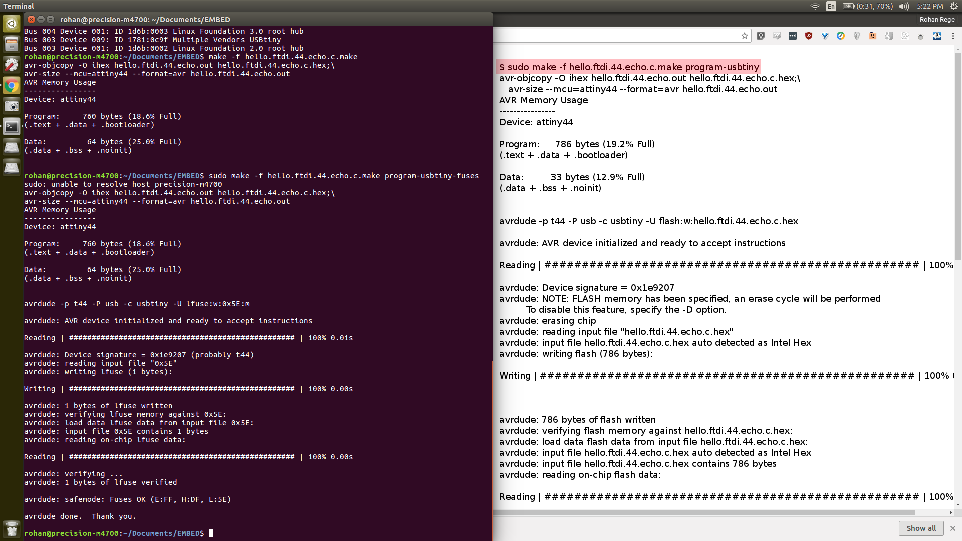
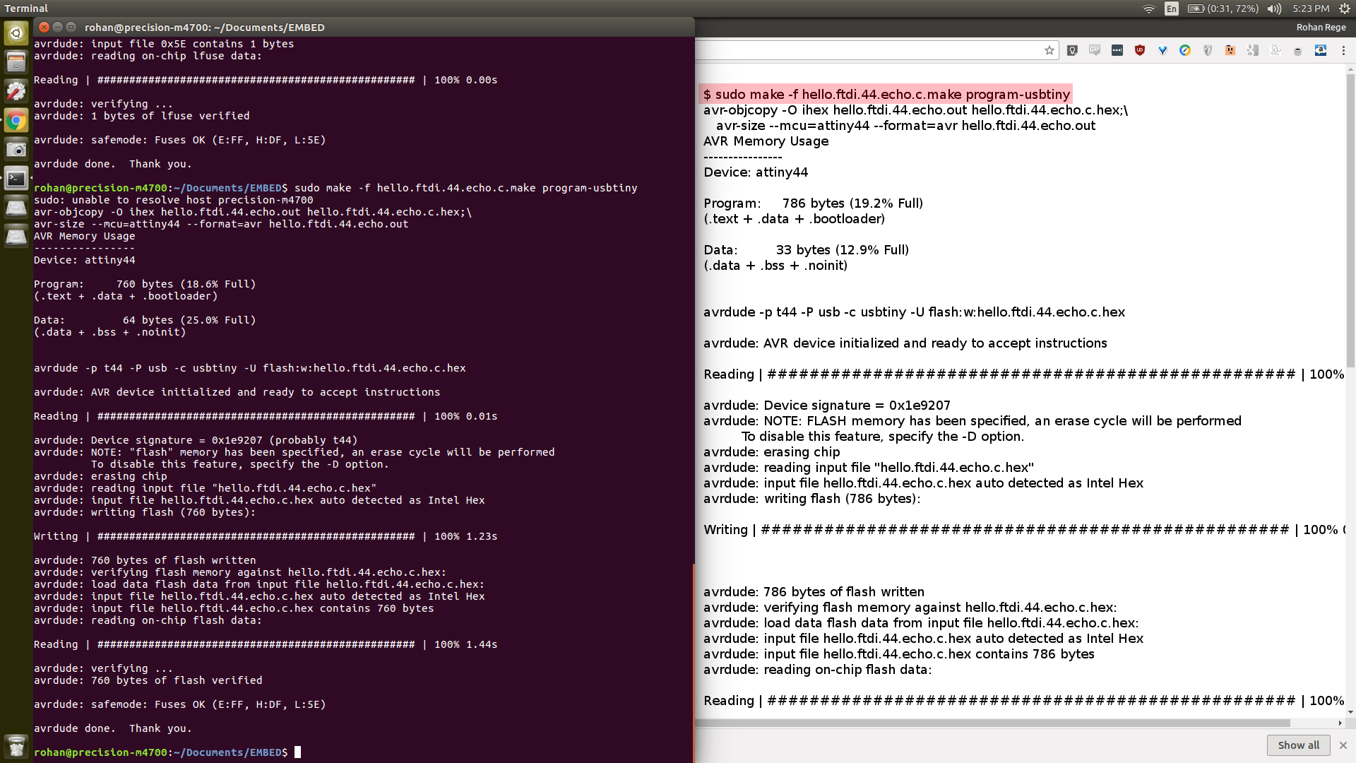
3: Then flashing the IC with the programme
4: Run term.py to get output
As you can see, the original "hello.ftdi.44.echo.c: you typed" is replaced by simply, "you typed"
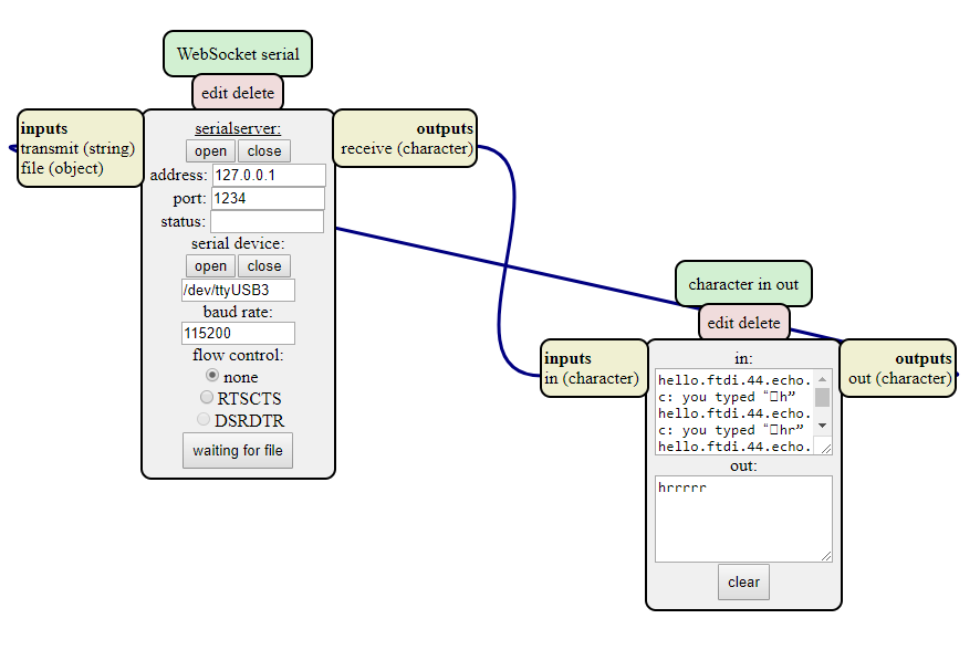
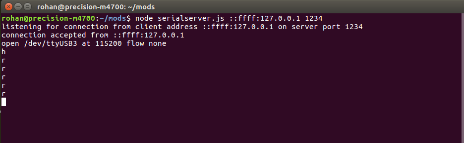
similar thing can be achieved by mods!
As shown by Neil in his video.
You need to setup a nodejs server to do this
Run the following command in the terminal $ nodejs serialserver.js ::ffff:127.0.0.1 1234 Remember on the website it is 127.0.0.1 (IPv4) but locally it is ::ffff:127.0.0.1 (IPv6)
Now the board is ready!
Group Assignment
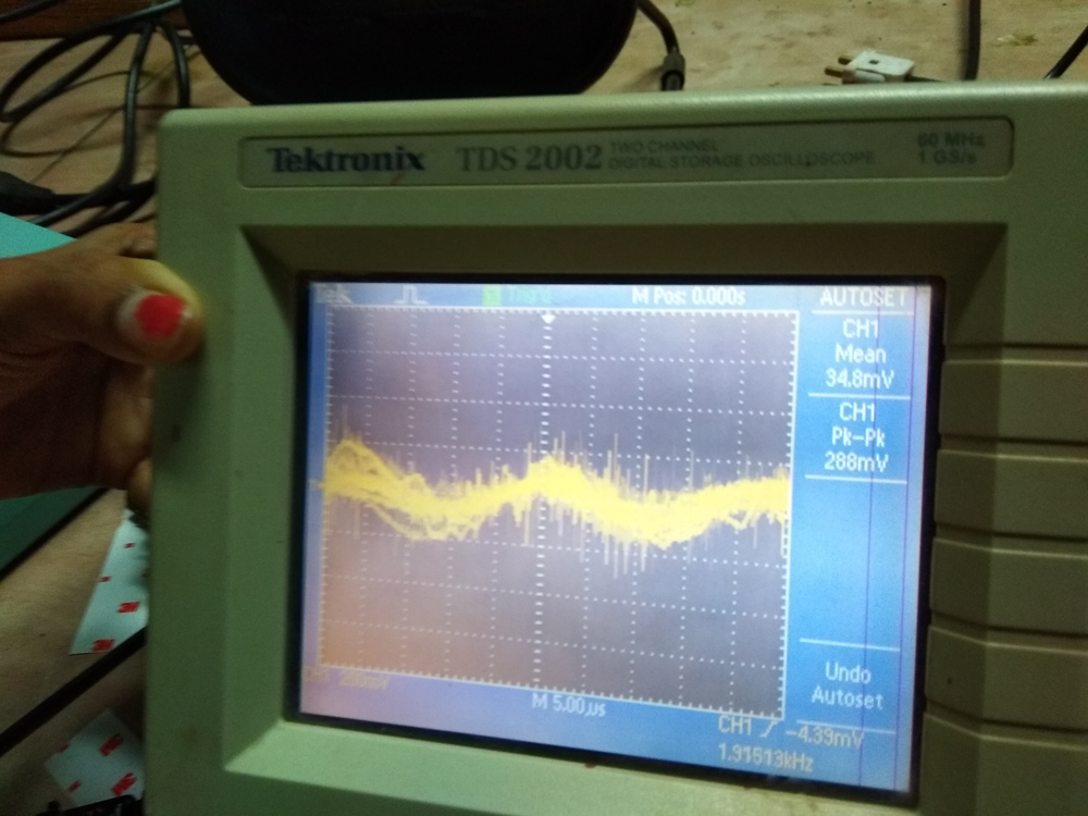
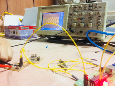
For group assignment, we did a simple testing using DSO, (Digital Storage Oscilloscope).
We tested Arefin's hello world board.
We were observing the voltage curves on his board.
Good soldering should give rectangular curve, but his board had wavy lines instead.
It denotes some problem in soldering.