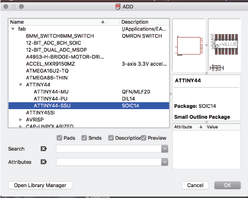
This week's assignmet was to modify the "echo hello world board", mill it and produce it. I started out by checking the original Hello_world board available online, and deciding where to put the button and the LED. I decided to connect the button to the reset pin, and the LED to one of the digital outputs of the AtTiny44. I used EAGLE from autodesk as a tool for redesigning my board. The first step was downloading the "fab library" from this link. Next, I started adding the components to the schematic.
The schermatic is like the "content" of the board. It represents the components of which it will be made, and how they will be connected to each other. Once all of the components have been added, the schematic looks something like this:
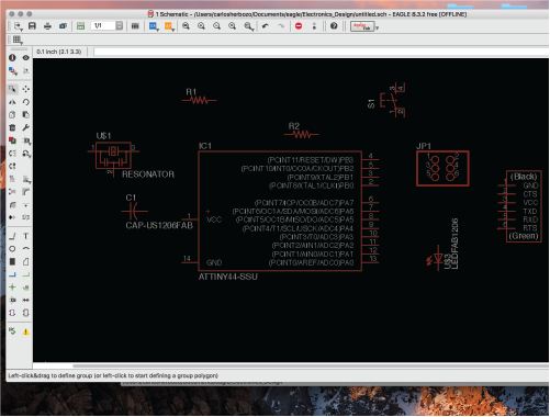
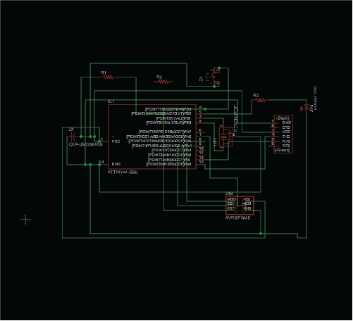
I then started connecting the components, regardless of the route each connection followed. Once everything is wired up, it looks kinda messy:
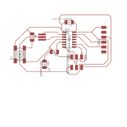
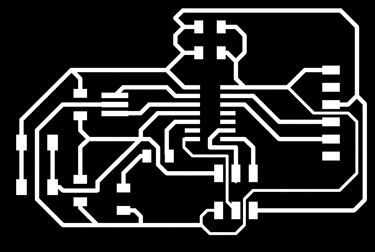
Afterwards, I switched to "Board" mode. Unlike the schematic, the board is like the "Layout" of the PCB. It represents exactly how the PCB will end up looking like. Within this mode, one cannot add or delete components, but one can move them around as convenient, and change parameters such as path diameter and board size. Once everything is moved up and routed, it looks like this:
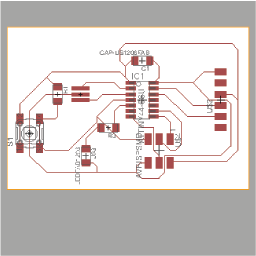
I then changed the dimension of my board, within the "dimension layer", so that the exported file consisted only of the PCB and not the extra space.
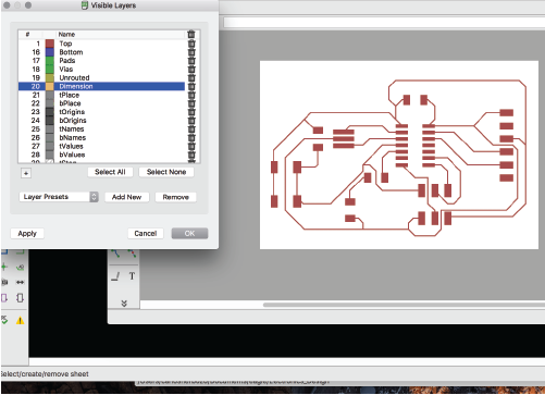
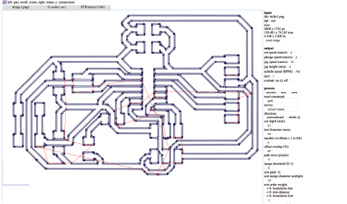
Finally, it was time to export my board as a .png. I did not use DRC for error control while designing my board, because I was confident I had designed the board properly, givwn how I had some experience doing this for my job. I decided to export as a .png because I wanted to try out "fab modules" as a CAM tool. The first step is seleceting the layers. In this case I only needed the "Top" and "Pads" layers, because of the SMD components. When using True-Hole, the "Vias" layer is added.
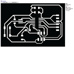
When exporting, it is necessary to select the "Monochromatic" option and add a high dpi count, so as to obtain the best possible resolution. I normally use 600 dpi. I uploaded my exported file to fab-modules and inverted the image. Because of the default settings of my Eagle version, my "board environment" has a white background, so it was necessary to invert the colors after the image had been exported.
I then changed some of the. parameters, like spindle speed (8000 rpm), cut depth (0.15 mm), coolant off, and tool diameter, according to the charactertistics of the machine available at the lab.
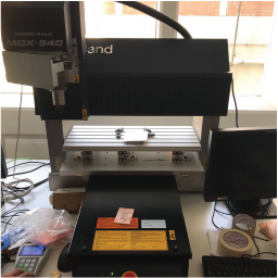
I used a Roland MDX-540 milling machine.
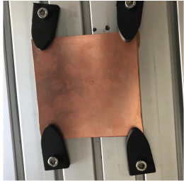
First, i secured the bakelite to the bed.
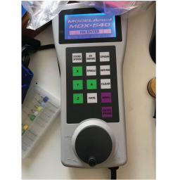
Then, I used the remote to set the origin point (G54).
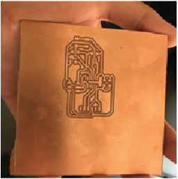
Finally, I sent the FabModules file to the milling machine, and here's what I obtained.
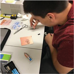
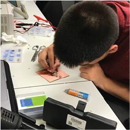
I then started soldering using flux and a heating gun.
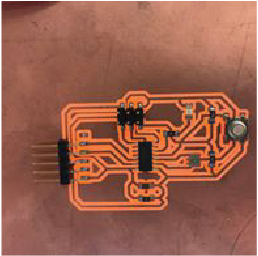
My board was completed!!! I tested for continuity to check that everything was alright, and it seemed ok. I'll wait for the embedded programming assignment to program and upload and verify its functioning.
You can download my files from the following links: