Electronic Design
Week 7
ASSIGNMENT
- Redraw the echo hello-world board
- add (at least) a button and LED (with current-limiting resistor)
- check the design rules, and make it
- optional: simulate its operation. Measure its operation
SOFTWARE USED
KiCad
winpc-nc
HARDWARE USED
1 ATtiny44
1 FTDI 3.3-5V
6 pin header
1 Crystal 20 MHz (resonator)
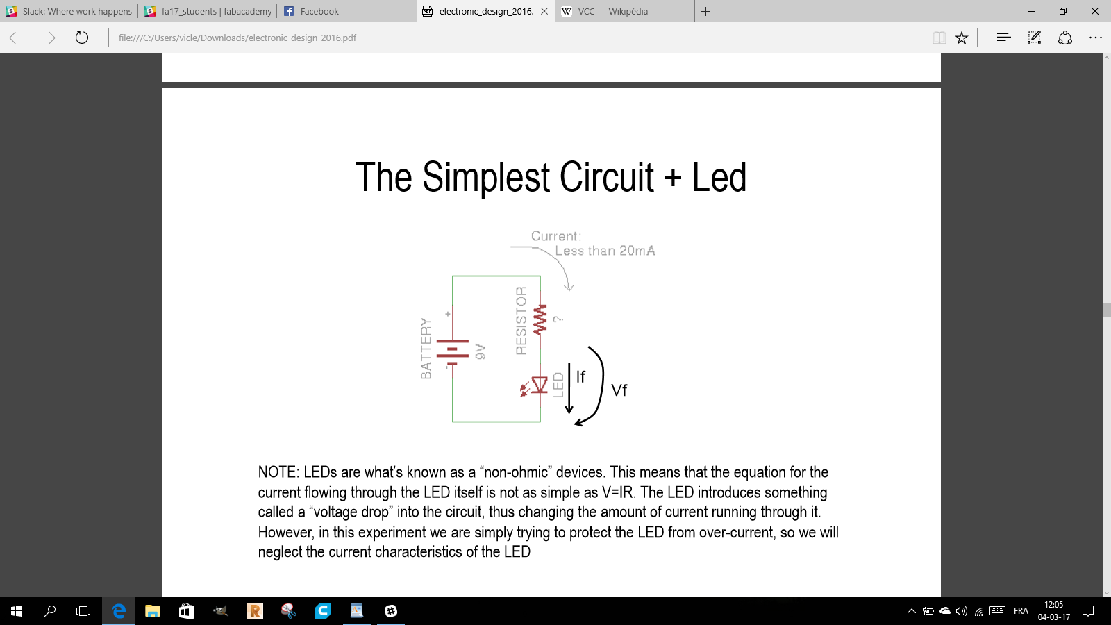
1 Resistor 10k
1 Resistor 499 ohm
1 Capacitor 1 uF
2 LED
1 push button SMD
LEARNING EXPERIENCE
This week I learned some basics of electronic,
I learned also to use KiCad to design an electronic circuit.
I learned to mill the board with a CNC machine,
and also learned how to weld.
For a better description of the pcb production with the milling machine:
see
FINAL PROJECT
FILES
Blink
Hello world KiCad
GROUP ASSIGNEMENT
electronic design group page
MAKING THE SCHEMATIC
I first read/studied the electronic introduction that Thomas, our instructor of last year, send us.
Not sure to understand everything, learning needs to be continued, again and again...
First I looked at an already made circuit to try to understand it
I took the list of components of Thomas's board
Opened a new schematic
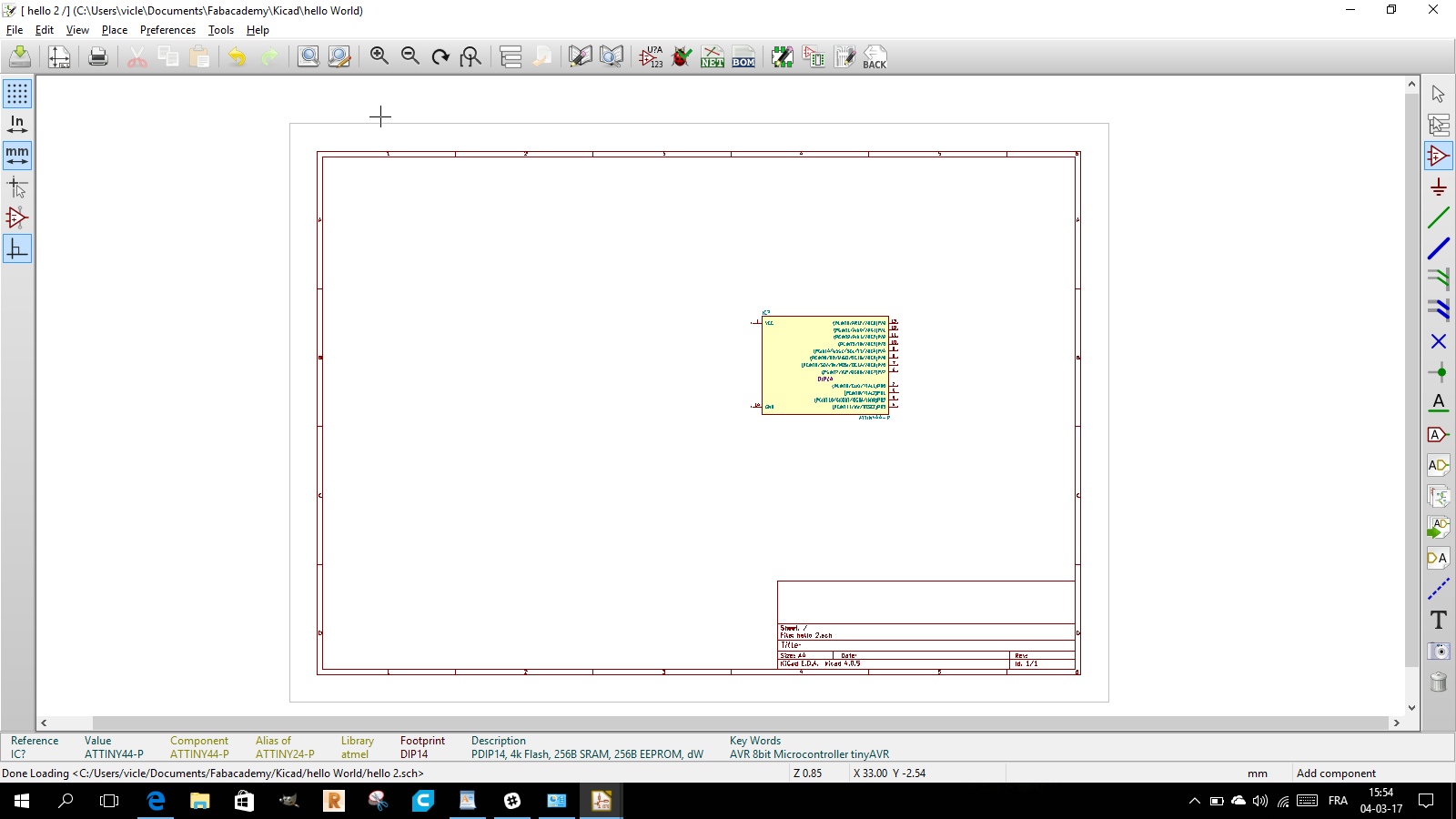
and placed the first component, an attiny 44 microcontroler
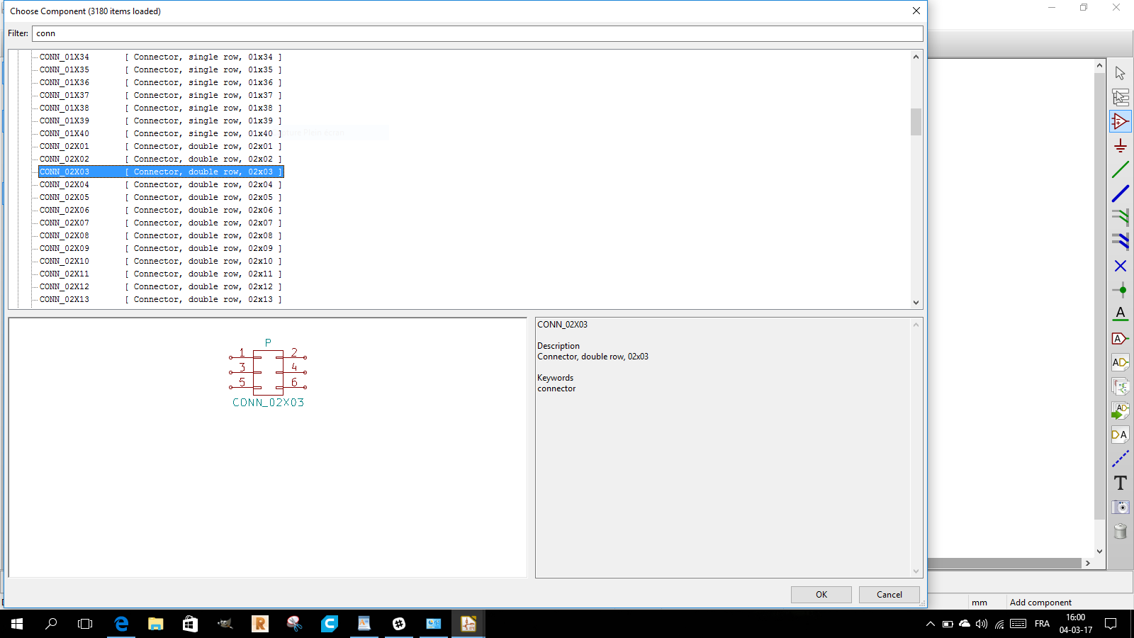
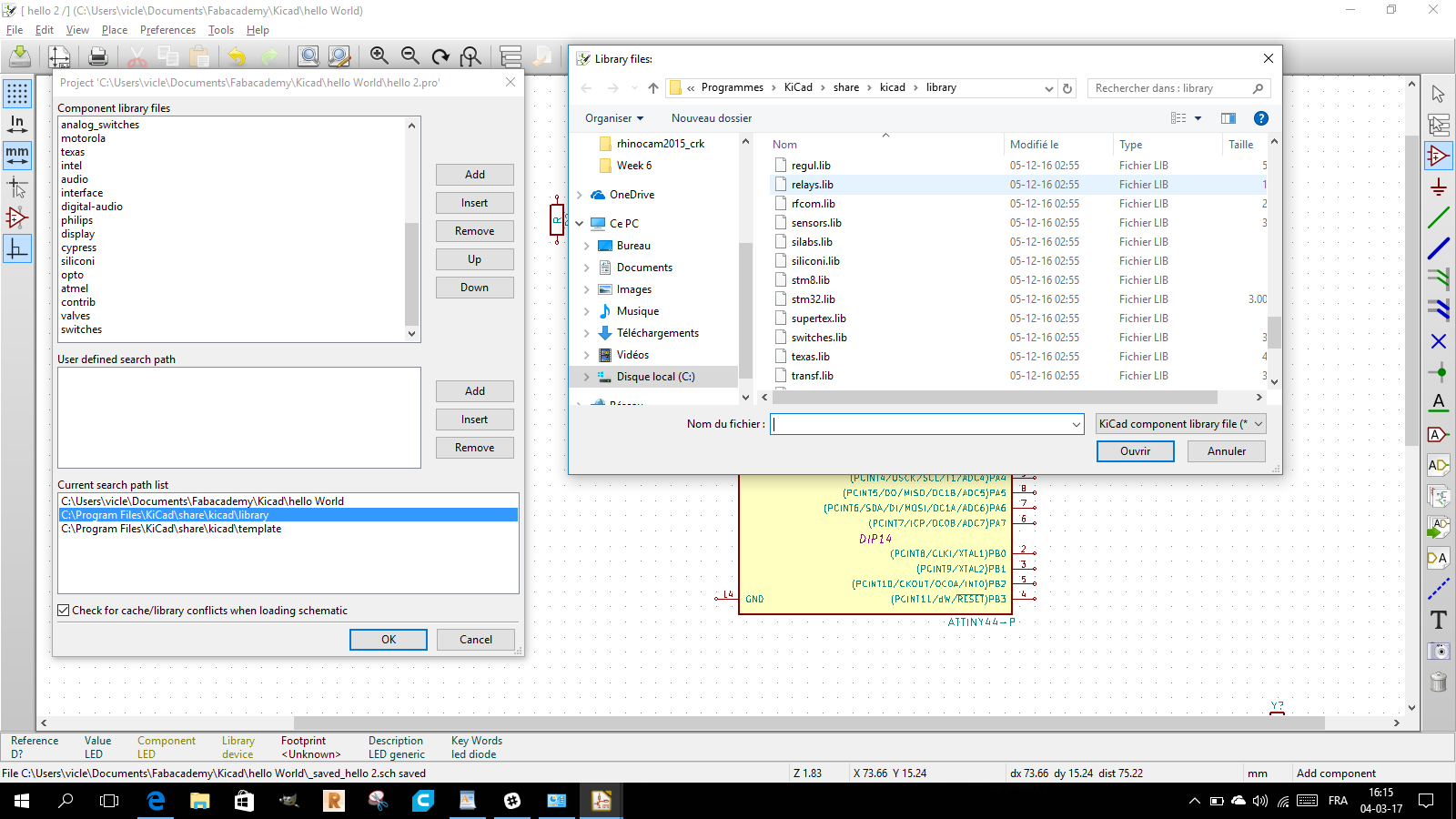
I searched the Fabacademy component library to upload in KiCad
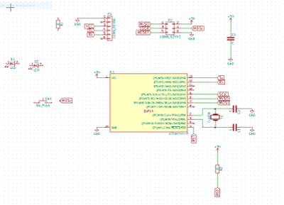
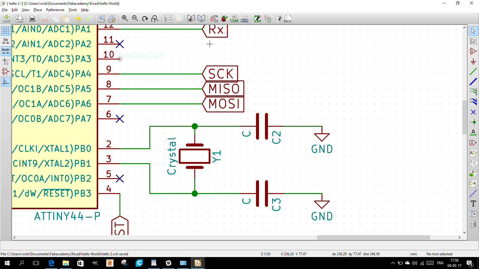
I placed the components and connected them together.

To connect at the right place, we had to research on the net how for example a ISP connector is made
I learned to use stickers to connect a pin and a component.
To do that you have to choose the sticker drawing tool on the left of the window,
You place the sticker, name it and connect it to your component.
You then duplicate it, and connect it to the pin of the microcontroller.
And finalised the schematic of the circuit
MAKING THE CIRCUIT
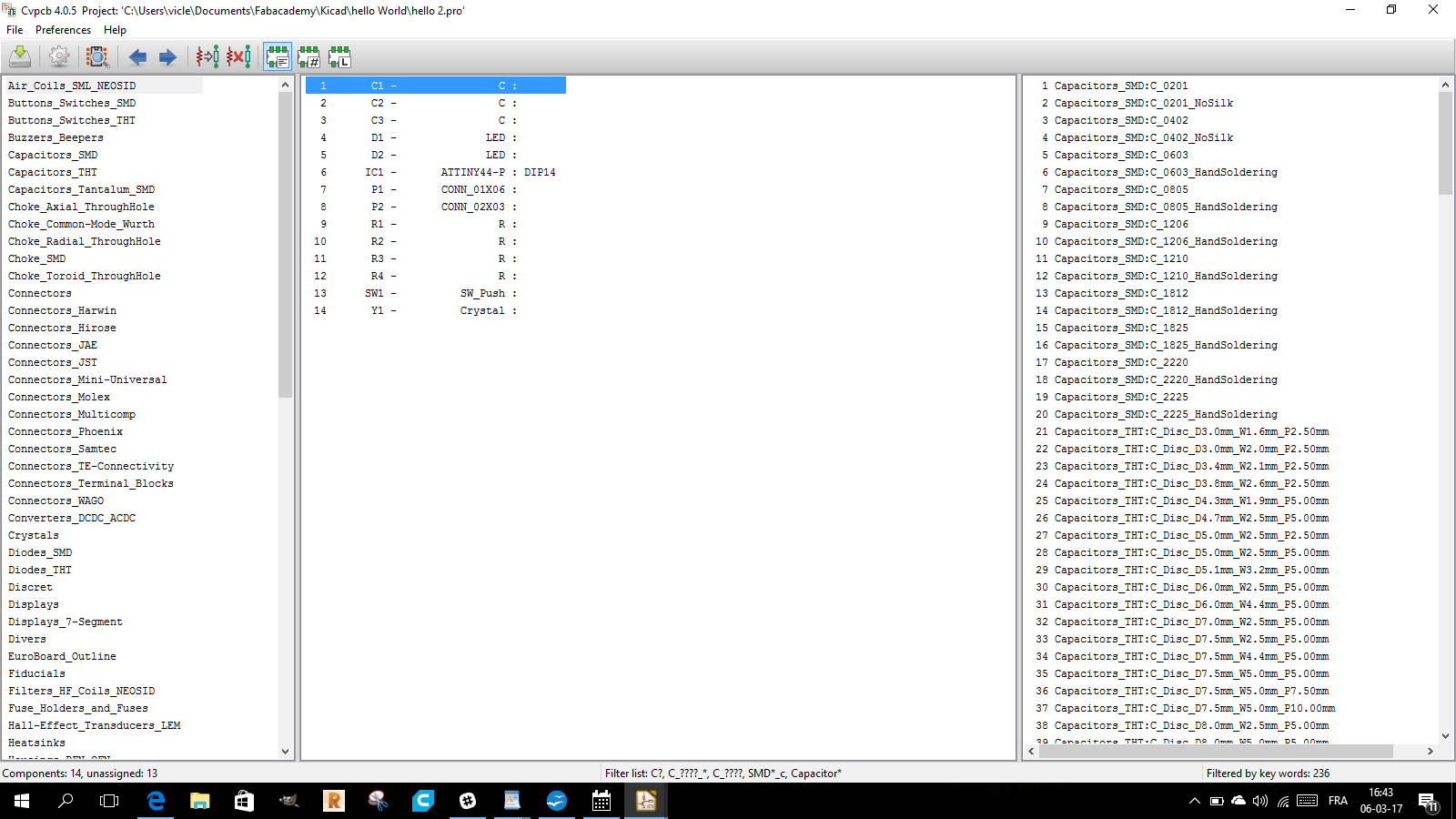
You have to associate the component of the schematic and the footprint of the component.
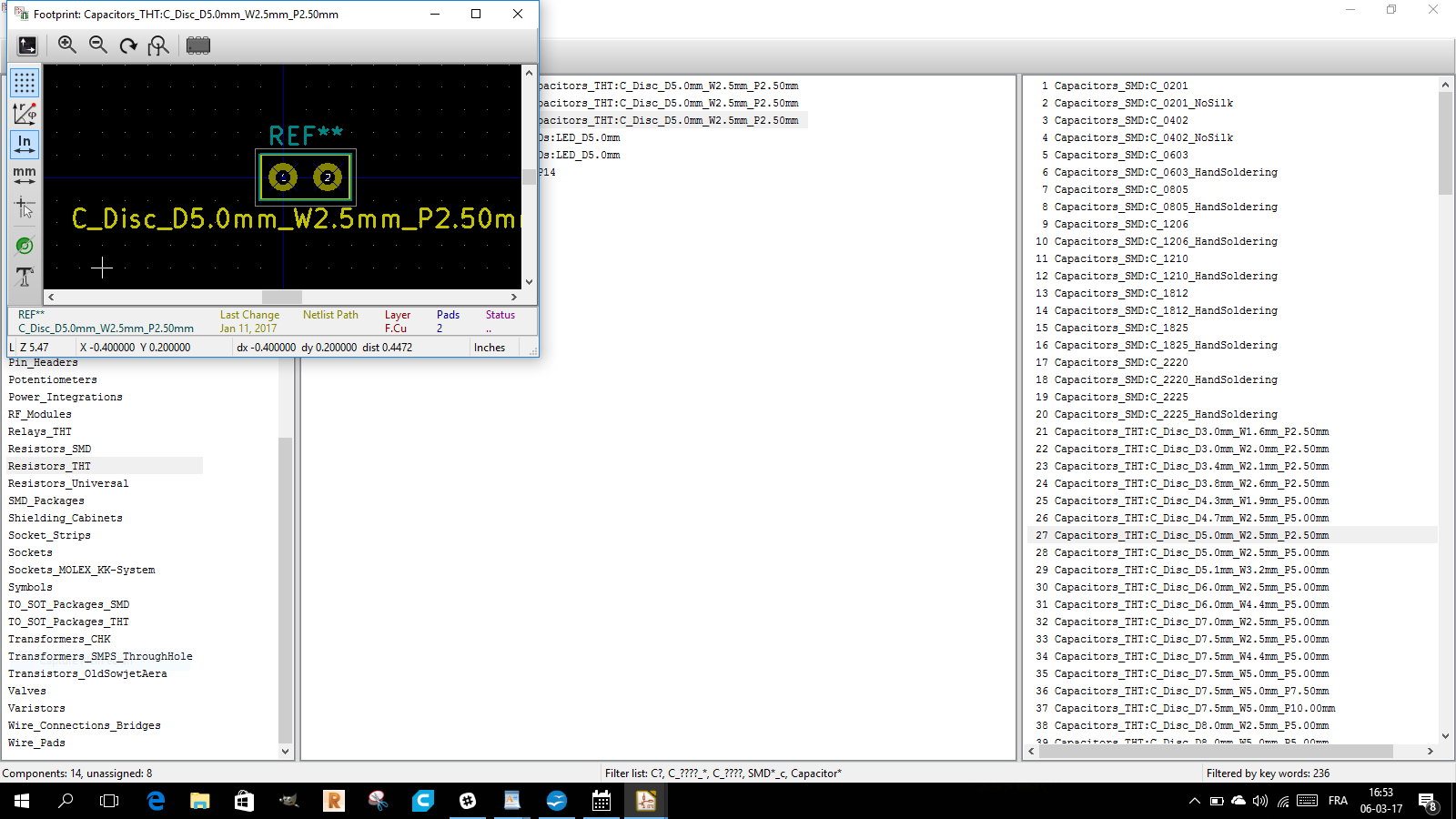
Looking at components drawings and putting the right components
I used the command
read netlist to generate the components and relations in a disorder way
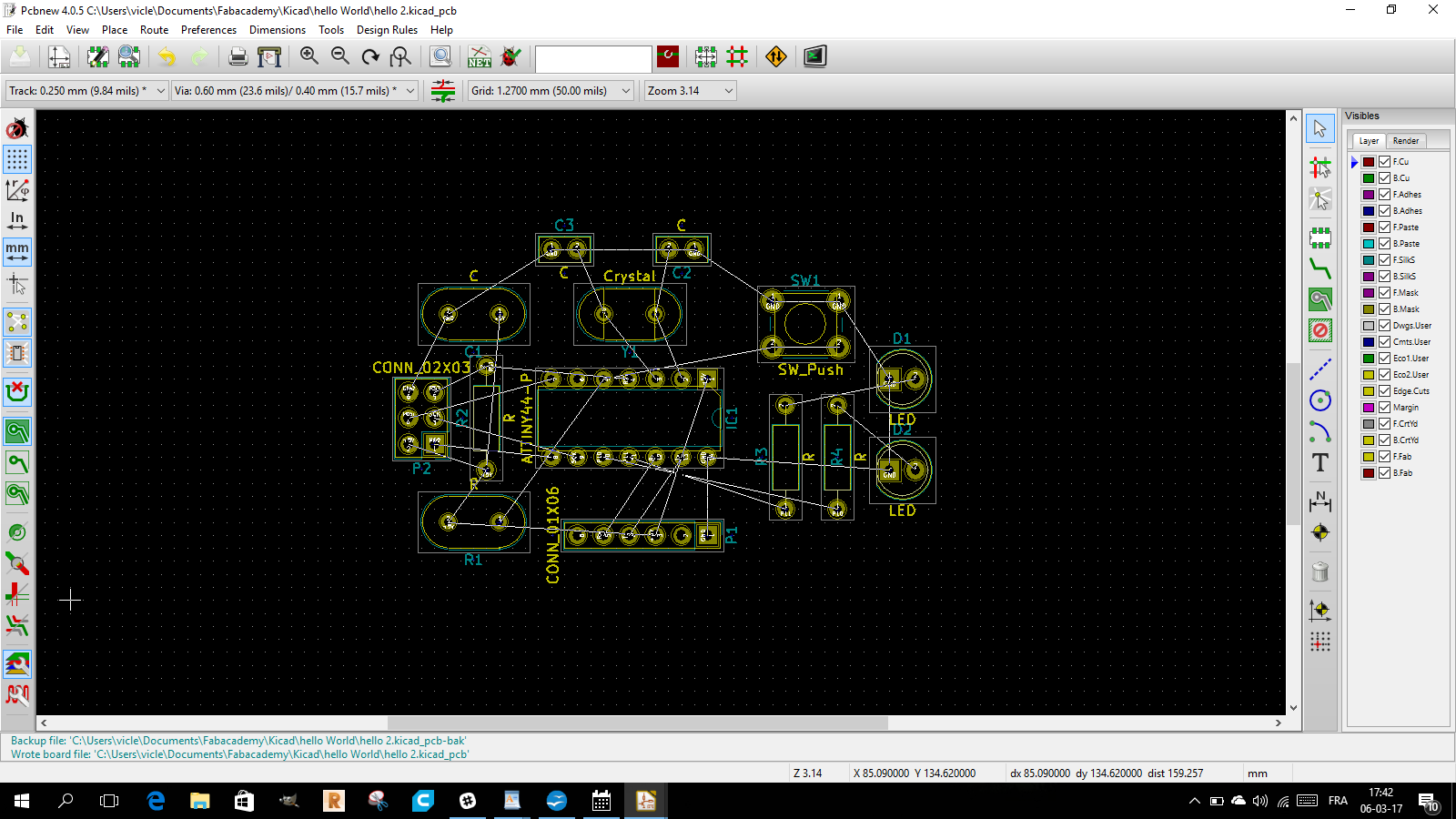
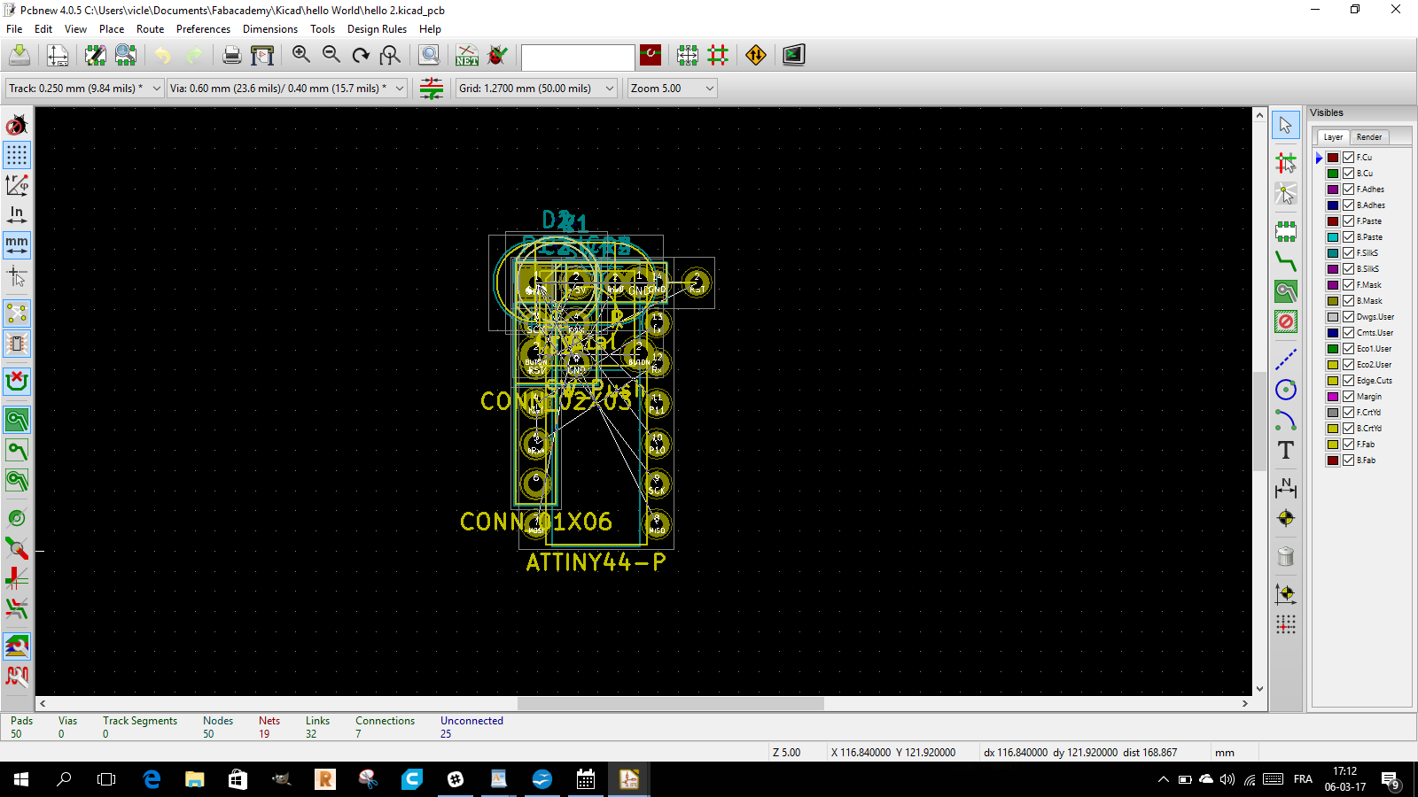
Changing place of the component to avoid crossing and put the component near the ones to connect
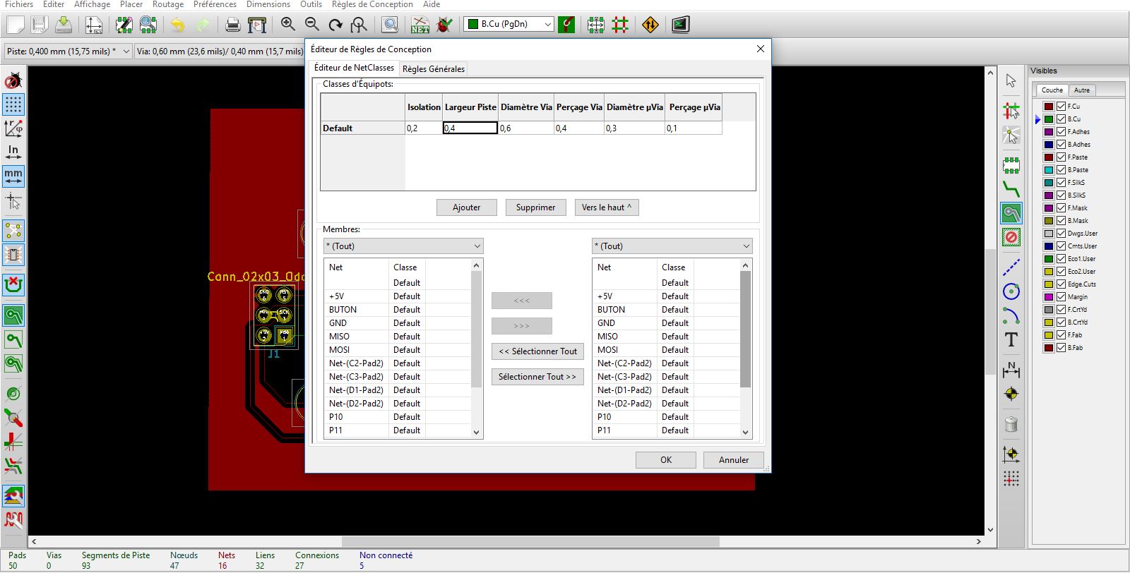
In KiCad, one of the important things to do before drawing the circuit is to determine the design rules.
Depending on the production technique of the PCB, it will be necessary to work more precisely.
In etching, we can be finer than on a cnc.
We will therefore determine the minimum insulation width between two paths, and the width of the paths.
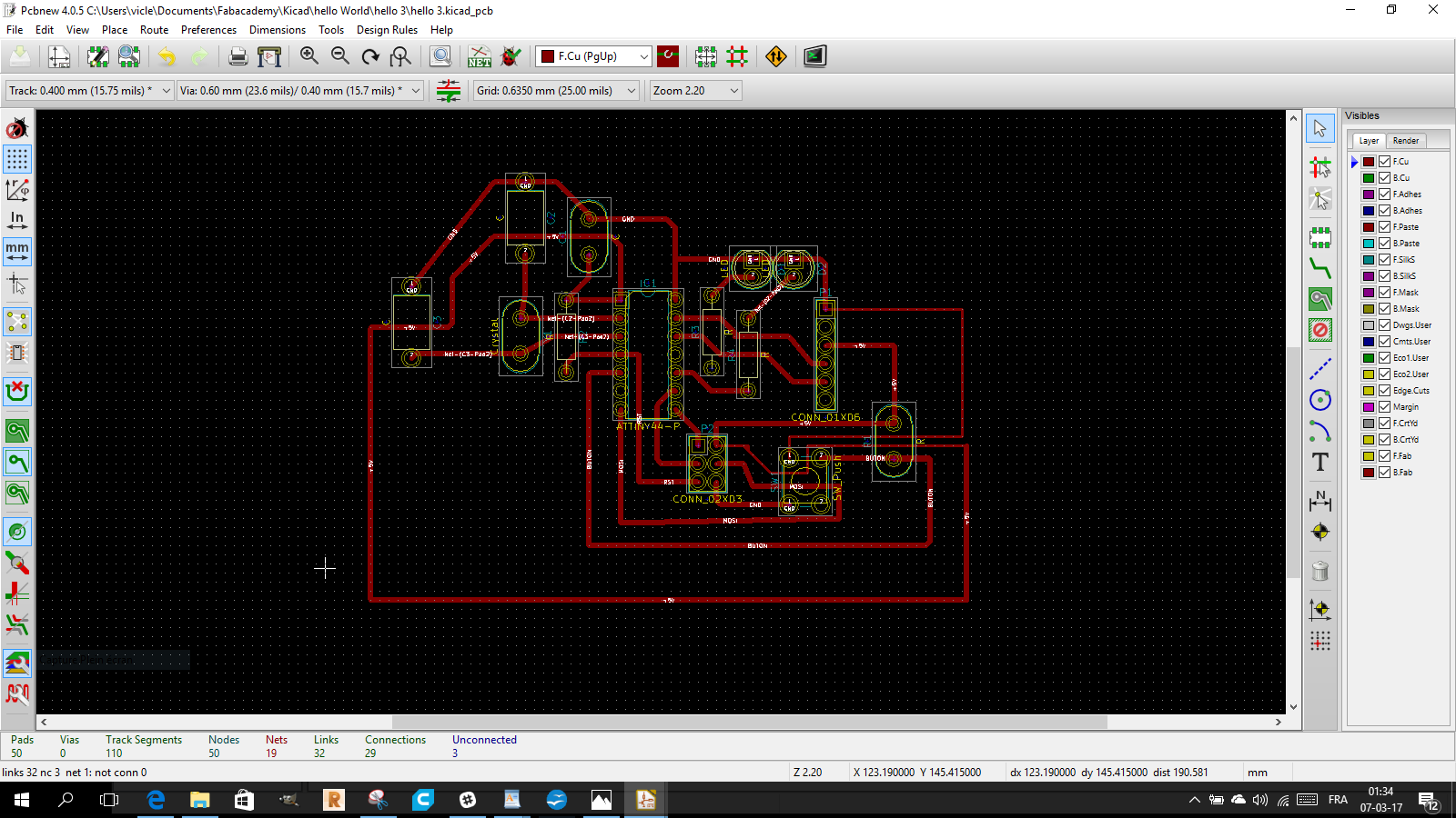
Here I chose 0.4 mm as width of path, which is already very fine to produce,
but which is necessary to pass between the connectors.
I also chose 0.2 mm of insulation between the paths.
I made the path to connect components, and finalised the circuit
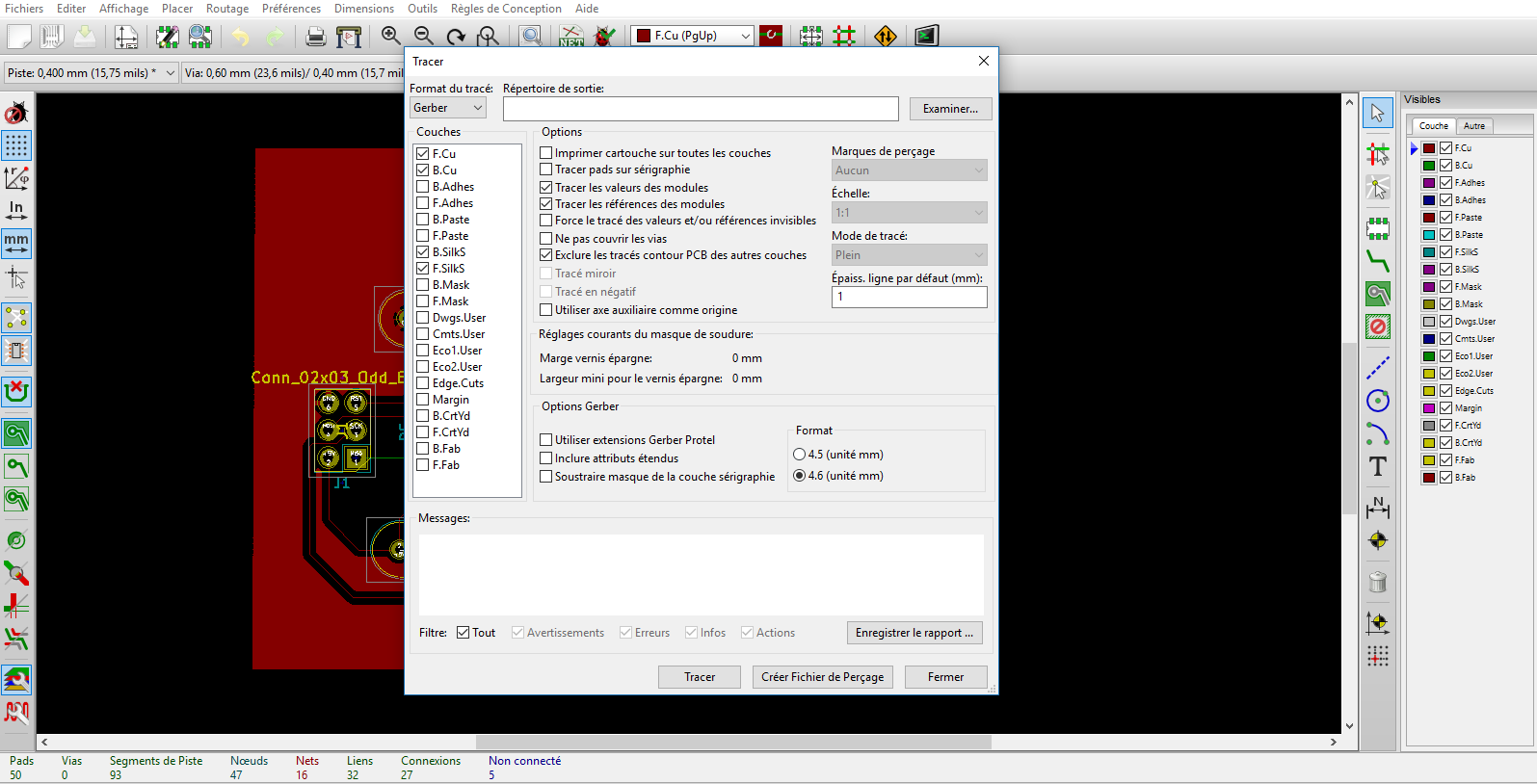
Made a Gerber and a drl files
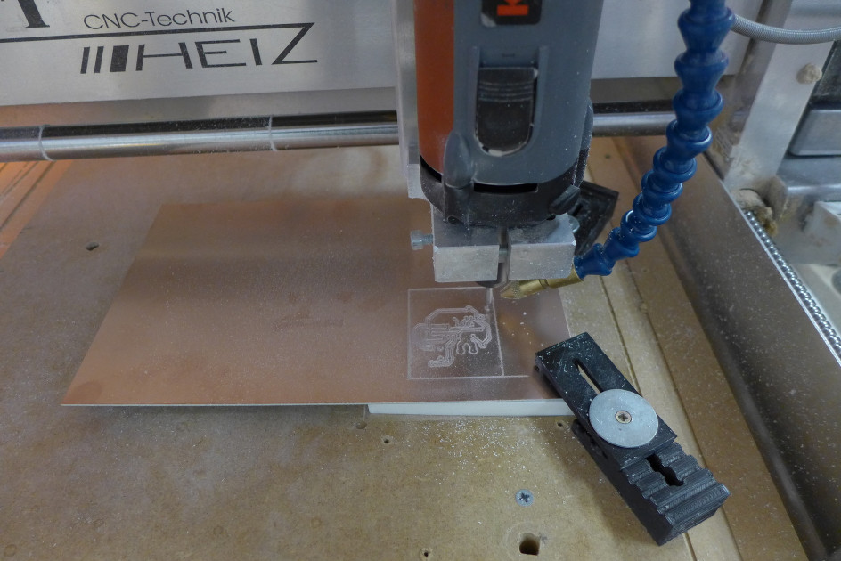
We went to Denis Lab to use the cnc milling machine for milling the PCB
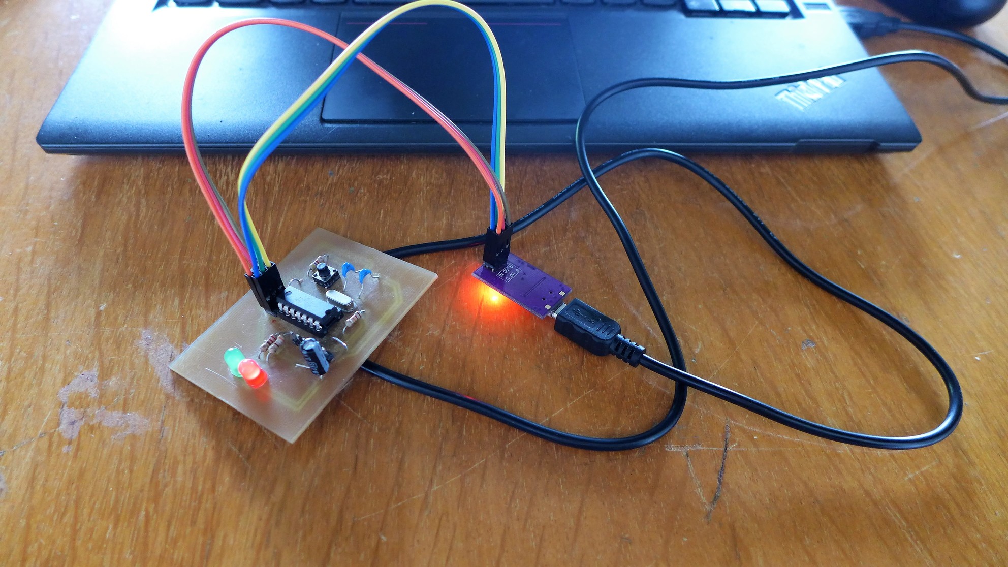
After that I Welded the components on the board
And wrote the sketch on Arduino IDE using blink example as a base
to make the 2 led blink with a delay of one second, one after the other
I had difficulties to put the sketch on the hello board
and succeeded with an usbtinyISP to upload the sketch.
 HOME
HOME