MAKE AN IN-CIRCUIT PROGRAMMER BY MILLING THE PCB
For this week the task is to make an In System Programmer(ISP) also known as In-Circuit Serial Programming (ICSP). This device is a programmer which is going to program other boards with micro controllers.This is what i understand in all before starting the week.Coming to electronics I am a total beginner and also well prepared with the fact that it will take time for me to get things right. Our electronics week started with a super lecture from our instructor Vinod kumar B.G. on basic electronics.That session went on for a full day which gave us courage to start with our week assignment.The next day our instructor Lancy Felix explained us about PCB,various types of PCB,PCB milling,milling and drilling operations,milling bits,soldering and about our week assignment. After the lecture sessions we were taken to the machine, the machine setting, milling and soldering operations were demonstrated to us and we started with our weekly assignment.
PCB FABRICATION
PCB or Printed circuit boards are circuit boards having copper clading which mechanically supports and electrically connects different electrical components.There are single side PCB's,double sided PCB's as well as multi layered PCB's available.In single side PCB's we have a copper layer above a substrate of non conducting layer.In double sided PCB's we have two layers of copper at top and bottom of the substrate whereas in multi layered PCB's we have alternating layers of copper between substate layers.In our lab we are using FR-1 type which is a single side PCB.In PCB's we can remove the copper and create circuit pathways by different methods like milling ,etching,plating,lamination etc.,in our lab we will be using the milling operation using Roland Modella MDX 20.
ROLAND MODELLA MDX 20
CHARACTERIZE THE SPECIFICATIONS OF YOUR PCB PROUCTION PROCESS
So this weeks group assignment is to characterize PCB production process
.For this we downloaded an image from the electronics lecture in the Fab academy website :
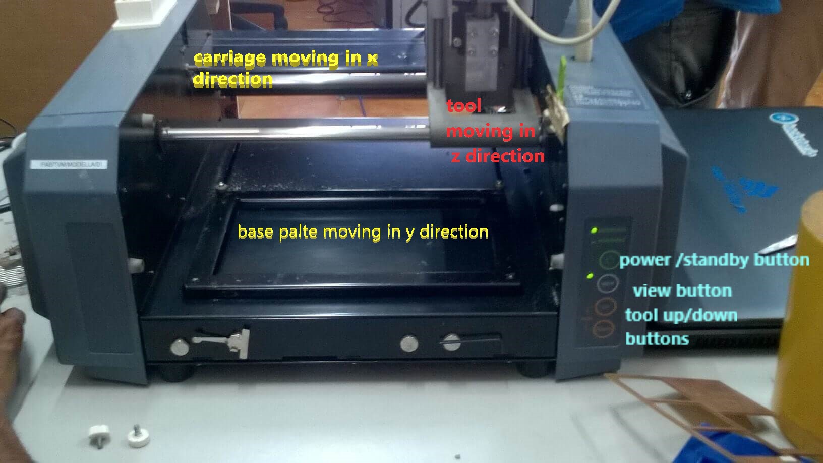
Roland modella MDX 20 is a desktop version of the PCB milling machine available
at our fab lab.It is compatible with most of the 2D and 3D CAD softwares.
It has a small bed which moves in the Y-axis, a Tool head
which moves in the X-axis and a bit attatched to it moving in Z-axis.We are using Fab Module software
to operate the machine. The input is mainly .png and output is .rmlfile. Image is always a black
and white layout of the board, the black portions will be milled and the
white portion is where the copper will be left.The main operations
performed by this machine are:
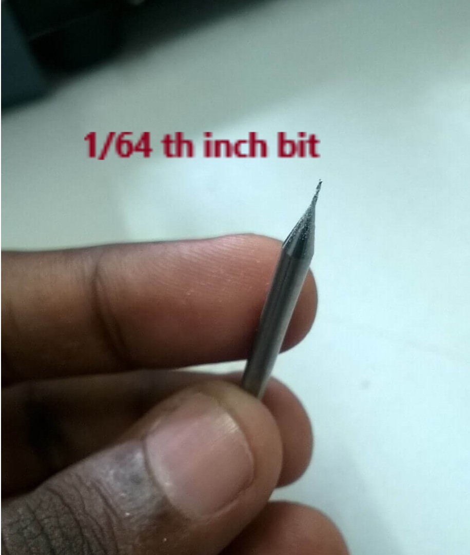
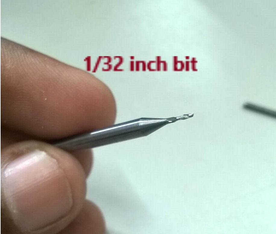
milling -to mill traces to get the circuit board pattern using the 1/64th inch (0.4mm) bit.
cutting -to cut out the board from the base copper clad using the 1/32th (0.8mm) inch bit.
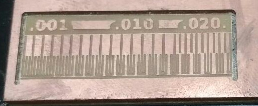
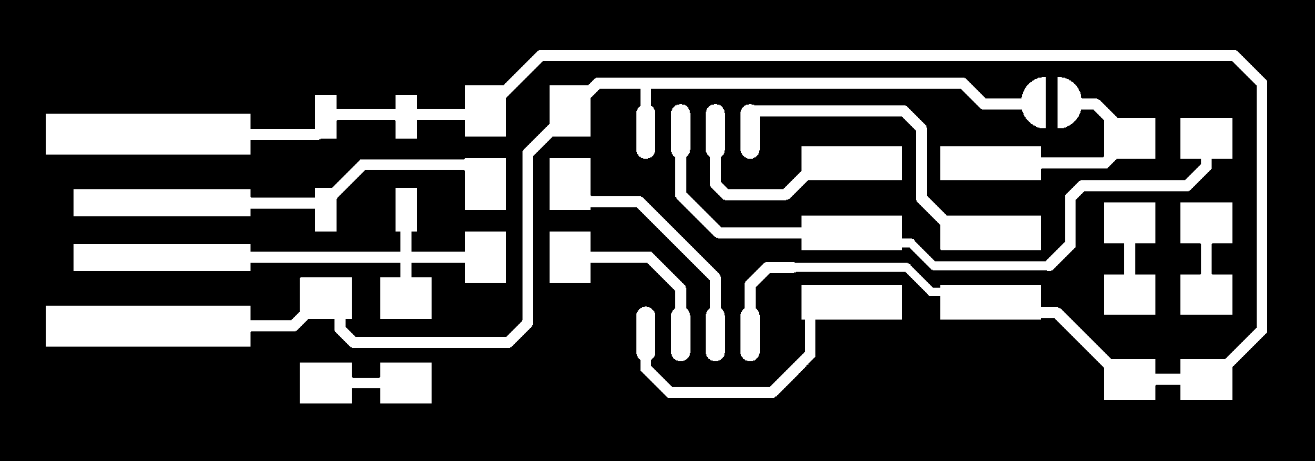
The Images for cutting and tracing are :
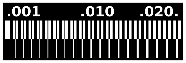
file used for milling

file used for cutting
For milling and cutting operations we have basic settings.
After milling and cutting operation
After the cutting operation it was noticed that one side has not cut,when we checked the trace it was a red line there, so we called our instructor he opened the image in gimp and tried with increasing its thickness then also it didnt worked.Now he rotated the images and performed the cutting operation once again this time the side was cut out perfectly
Group assignment
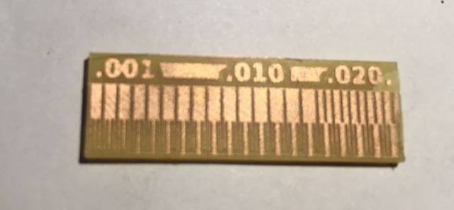
We found out that the The 1/64th inch (or 0.016") bit in our machine could not trace the lines of thickness 0.001" and 0.01". This may be due to the wear and tear in the bit and aging of the machine.
MAKING ISP BY PCB MILLING
So this weeks assignment is to make an In-Circuit programmer by milling
the PCB.So the basic steps are:
1).Selecting the ISP
2).Setting up the machine
3).PCB MILLING
4).Soldering the components to the PCB
5).Checking and debugging the PCB
6).Programming the PCB
Selecting the ISP
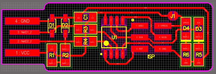
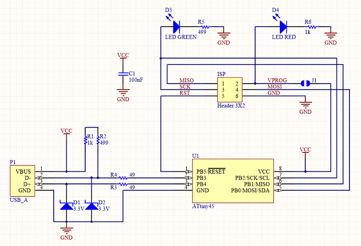
For this week Assignment we are having different ISP designs available at the Fab Academy site and we have to choose one and I am choosing .The component and schematic diagram of Brian's ISP are shown below:
Setting up the machine and PCB milling
The setting and operations of the milling machine are as follows:
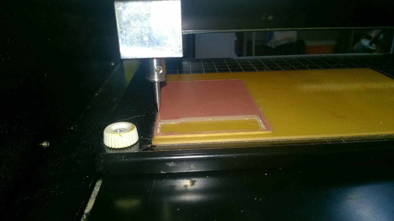
1).The machine has a base metal plate on to which we have to paste the PCB for cutting.So in between the metal
plate and the PCB we have to put some layer to reduce the risk of bit hitting the plate.this layer is known as
sacrificial layer.You can use another PCB as sacrificial layer.
2).The PCB as well as the sacrificial layer is fixed to the base plate by using double sided tape.We
should be careful that while pasting there should not be any air bubble as this slight variation in level can
affect the milling operation
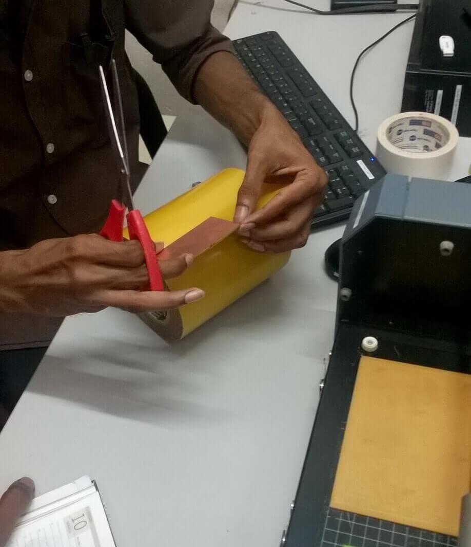
Fixing PCB using DOuble side tape
3).Switch on the machine,load the fab modules(we are using the offline version in our lab). Select the trace for milling,give the output option and for tracing choose 1/64 bit.
traces for milling the PCB
Now for milling the offset ,speed and depth are already set we just have to note down the x and y position
for performint the cutting operation.
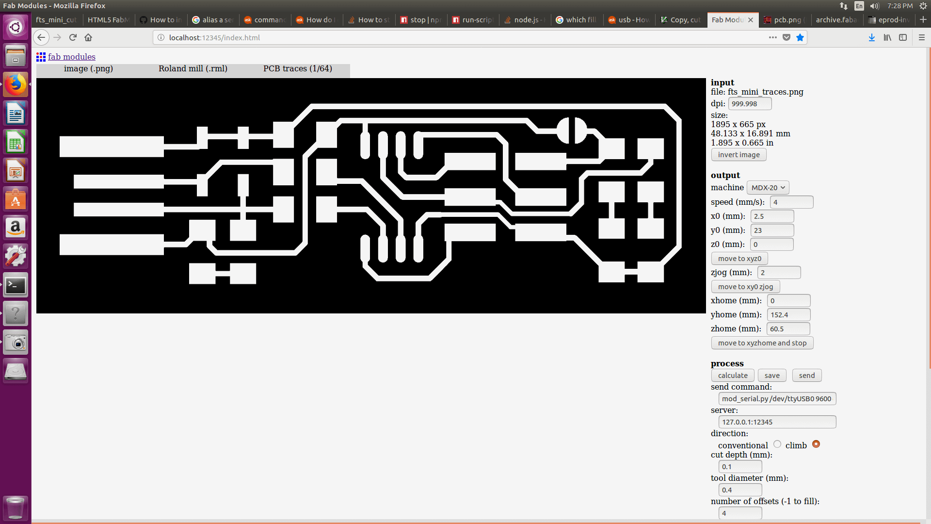
FAB modules print manager window
4).Now press the view button on the machine.The plate will come front and the head will move to right.load the 1/64 inch bit to the head .While loading the bit always put a sponge
at the bottom to add an extra safety for the bit, if it falls.We are using allen key to fix the bit on position.
5).Now press the view button again to move to (0,0)position.Use the x and y values in the print manager(fab modules)
to correct the position of bit with the PCB.It is actually a kind of trail and error process.
Gravity fixing of the bit
6).Recheck the space left in the Z axis for the bit to move down,also if the bit is touching the material and start the operation.
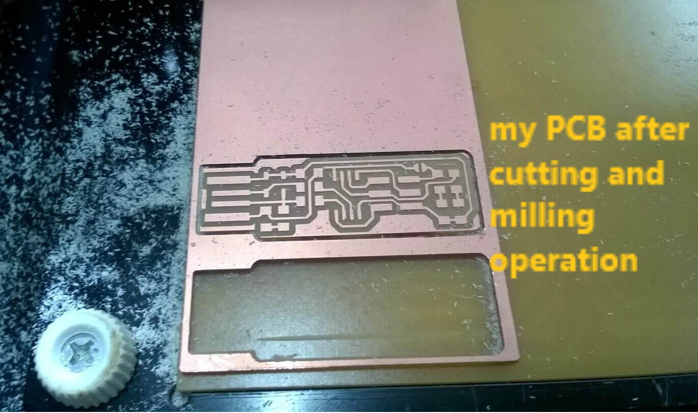
7).After milling operation, load the png file for cut.


load the 1/32 bit,give the x and y values and perform the cutting operation.
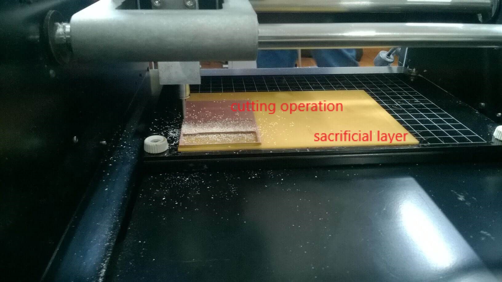
8).After the operation we have to vaccum down the dust using a vaccum cleaner.
Sodering the components to PCB
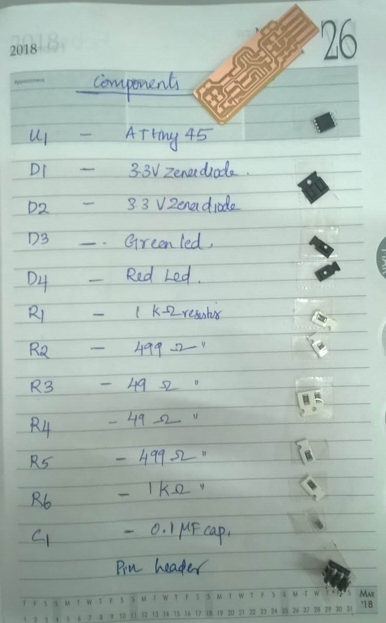
The components needed for making the ISP are listed below:
1) 1x ATtiny45 or ATtiny85
2) 2x 1kilo-ohmresistors
3) 2x 499 ohm resistors
4) 2x 49 ohm resistors
5) 2x 3.3v zener diodes
6) 1x red LED
7) 1x green LED
8) 1x 100nF(0.1 microfarad) capacitor
9) 1x 2x3 pin header
While Soldering always make sure that the surface of copper is cleaned and it gives a
shiny finish,or we have to just rub with the cutter blade to make it shiny.
Mistake
Do not exert more pressure while cleaning the surface,I actually got a cut in my PCB and later soldered to join
that break.
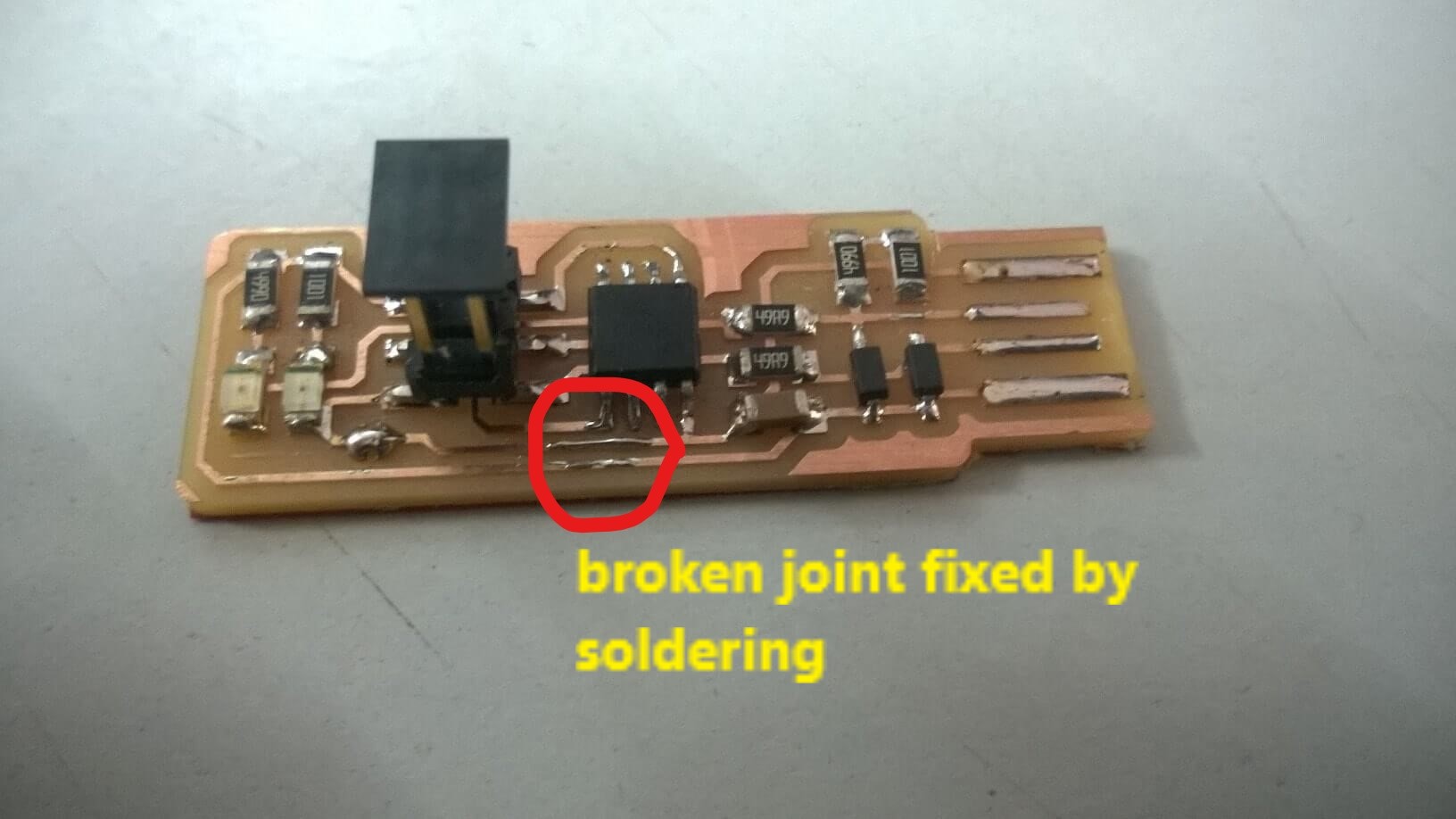
Remove the unwanted traces in our PCB with a tweezer
Solder each component safely that it ensures a good seating on the PCB.
In our circuit we have to create a bridge between J1,so that it can beused to program the ATtiny 45
AFter soldering the components.

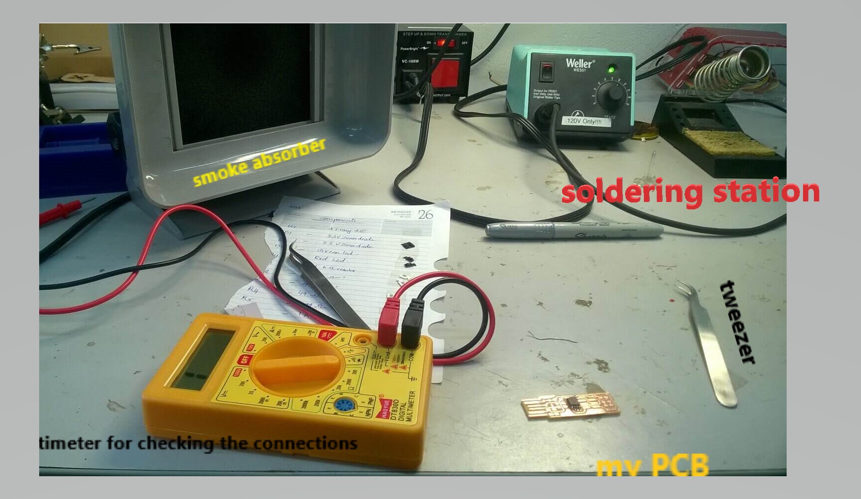
Checking AND debugging the PCB
After soldering each component we have to check it using a multimeter.If the connections
are proper it gives a beep sound for the components,for diodes it shows thhe value,and for leds it lights up.while
debugging with the multimeter i found out a loose joint in one of my legs of the ISP header pin and was able to solve the issue.
After soldering, inorder to increase the thickness we stick some vinyl layers at the back.inorder to gave a tight fitting,
when connected with the computer.
Programming the PCB
So inorder to make the ISP we need to program our PCB.Since i am using windows,eventhough the
steps are hectic,I decided to give it a try using the GNU AVR toolchain in windows 10.
Since i have already installed Git i went on to install ATmel GNU toolchain but the download link mentioned is showing
404 error.
Then i searched in the website for it and installed it.Following the steps I installed GNU make,avrdude,and updated the path
by going to the control panel and added the path files
Now we have to Install the Driver using Zadig Using the dowload link.Now plug in the programmer and install the driver
After performing all these steps we have to perform the sanity checks mentioned in the page using gitbash.All the checks were performed
and it came out well.
After that Download the firmware and extract it.
After all this during flashing an error message popped opt showing the programmer could not be found.At last I left windows and
started my work with linux.
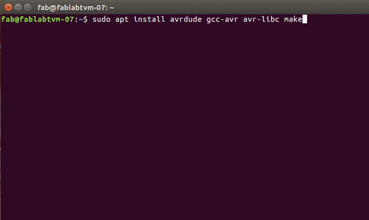
Programming with Linux
I used pc at our lab for making my ISP.The first step was to install the compiler,library for compiler,flash,and make for storage of main function by typing
sudo apt install avrdude gcc-avr avr-libc make
After that we need to download the firmware as mentioned in the tutorial.Extract it and open the terminal.
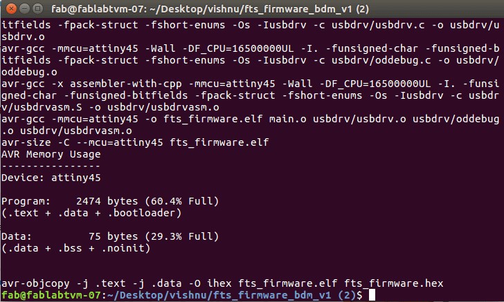
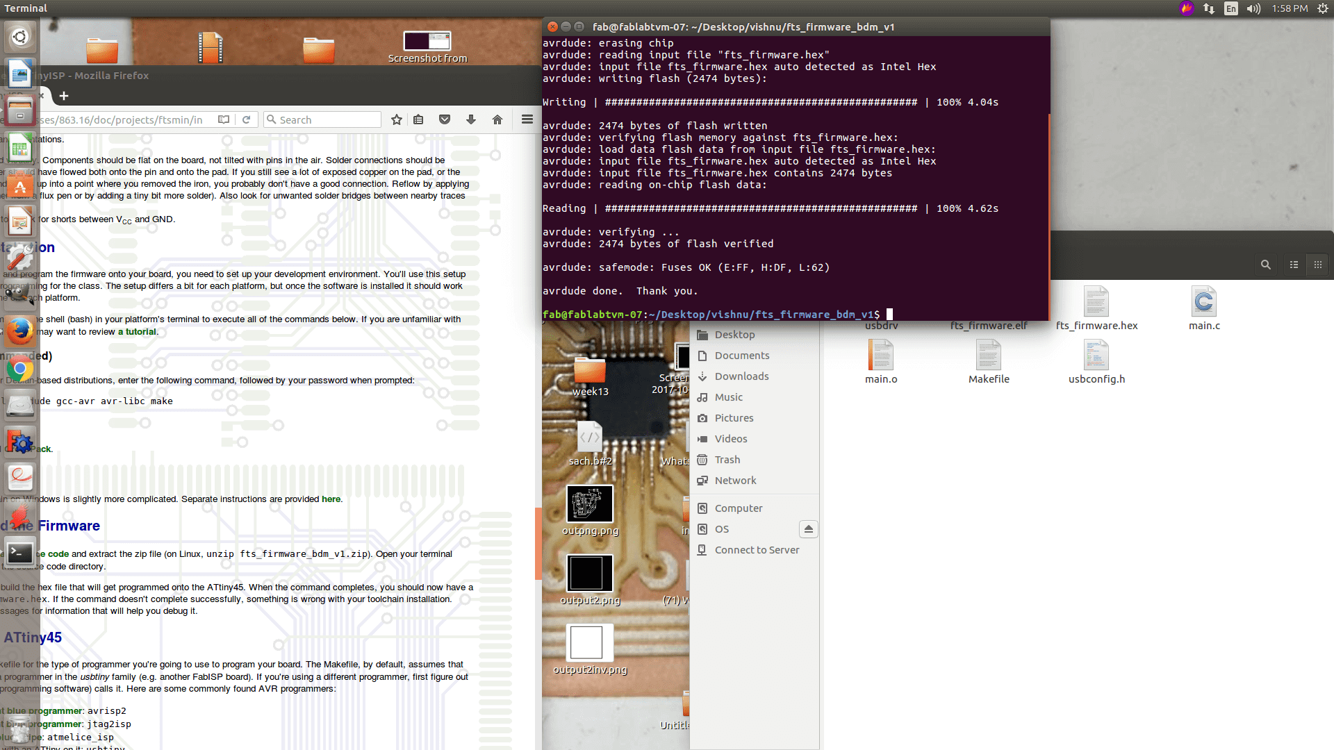
Now run the make command to make the hex file. named fts_firmware.hex. Now we have to plug in the ISP and connect our PCB to it.Check the name of the ISP inside the make file is usbtiny.else give the name as such.

Now run make flash command which will erase the PCB chip and program its flash memory with hex file we created using command make flash
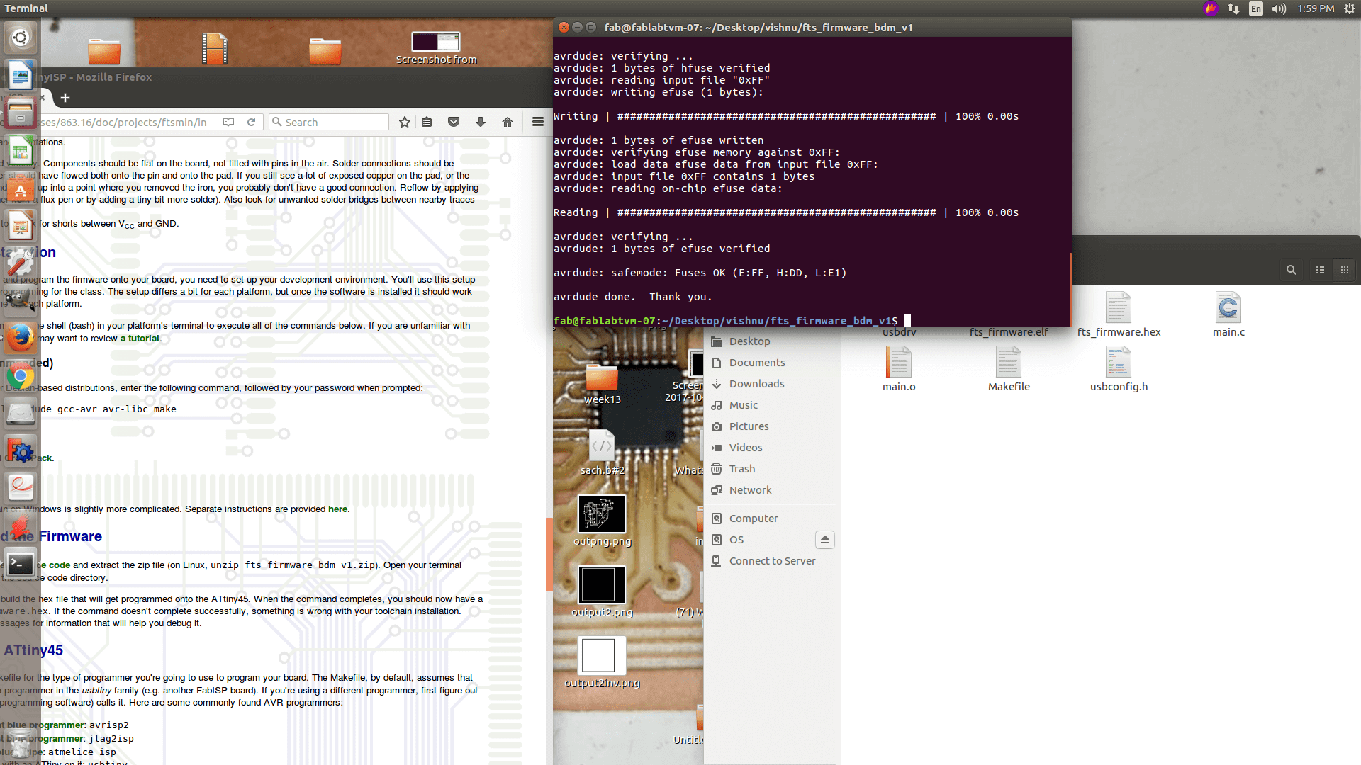
Now run make fuse command to set up all the fuses.
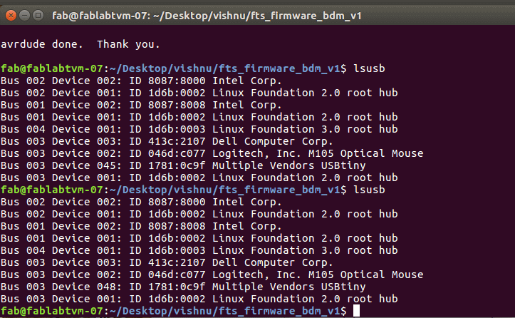
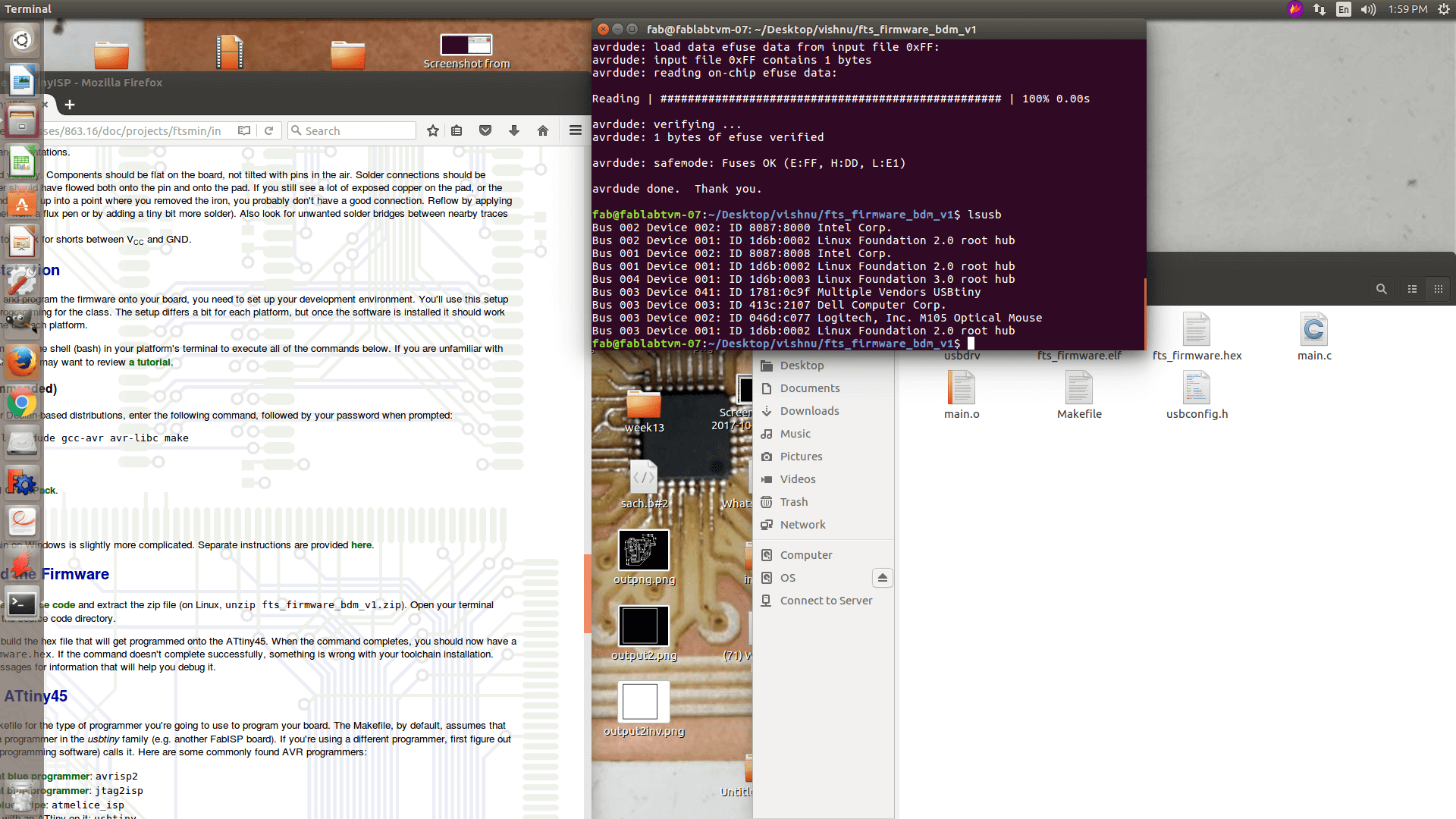
Now list USB using lsusb command.
Now run make rstdisbl to disable the reset function in the PCB, so that it can now be used as a programmer.