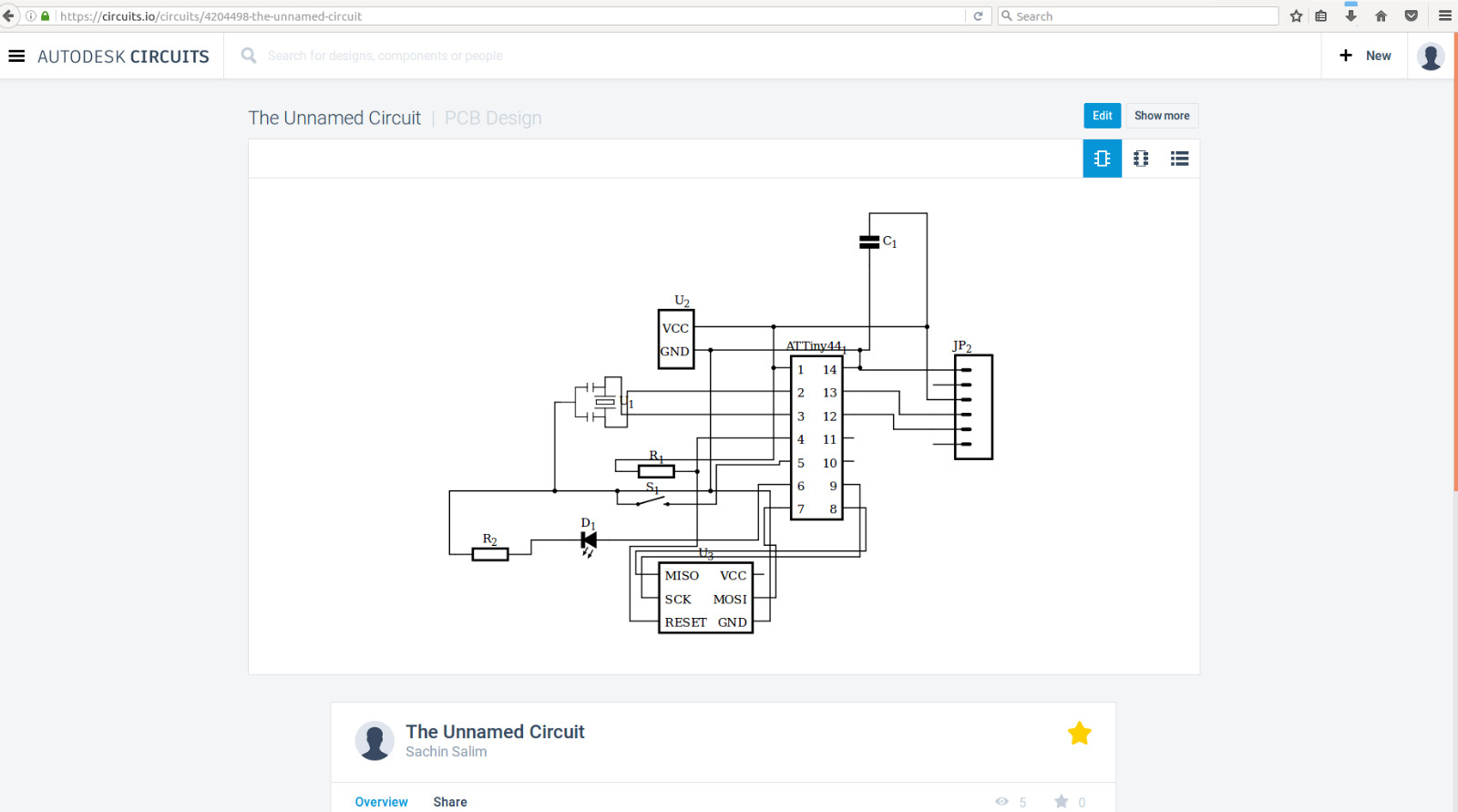
This week our assignment was to familiarise with some circuit designing softwares and redraw echo hello world board and add some additional components in it, atleast an LED and a switch
Eagle
Eagle was the first software I tried since Im much familiarise to it. I downloaded it and the installation process is not as much as hard
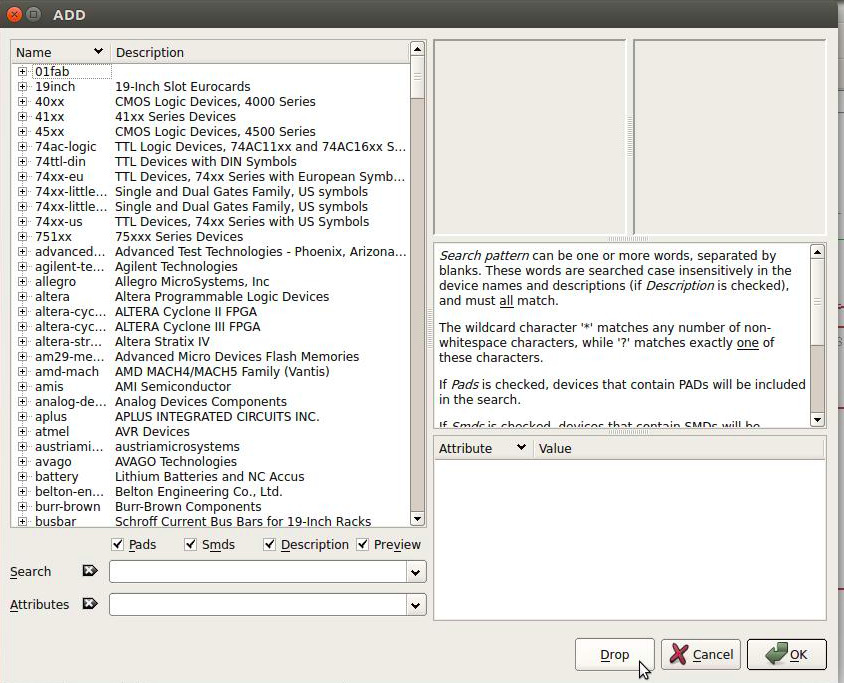
For this first of all we have to add fab library in eagle where almost all the components are there available for our assignment.
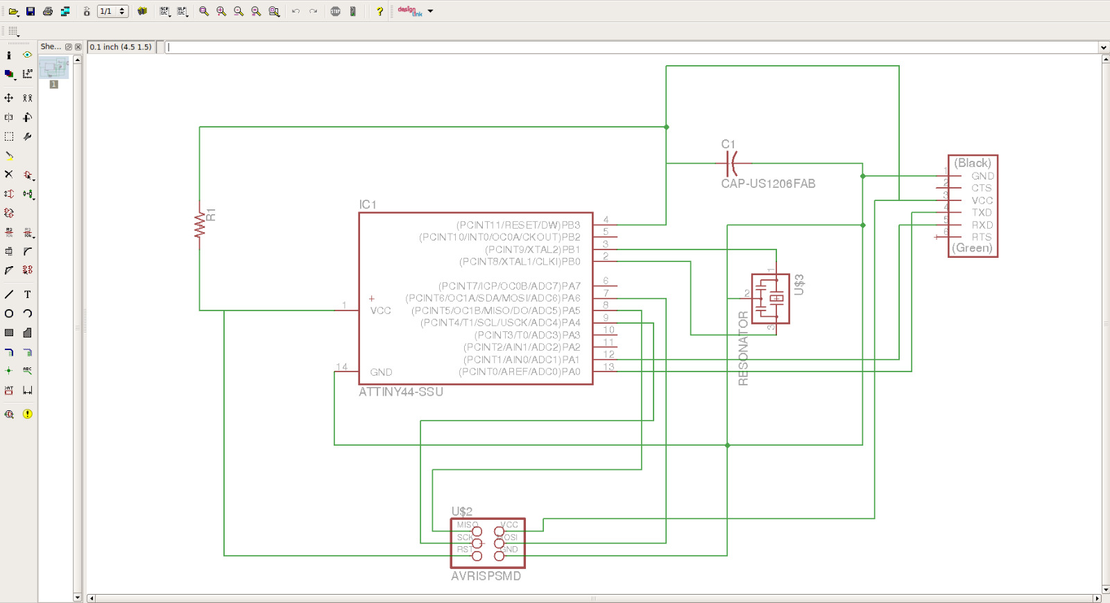
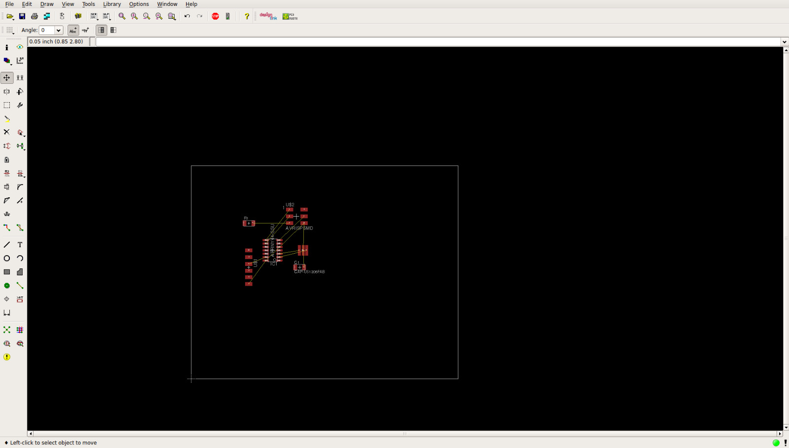
Then we should draw the schematic in such a way that each components are added and then connect them each other using wire as per our design.
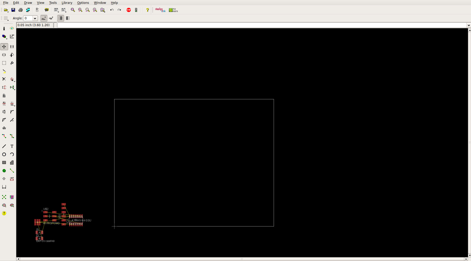
Ater that what we have do is that we have witch the schematic to board layout.
There we can see that there should be components as we added scattered outside a rectanglar space. We have to pull all the components into the box where we can see that all those are interconnected and the arrangement in a packed way so that only a small space have been occupied when routing. Routing is a step in the design of printed circuit boards (PCBs) and integrated circuits (ICs). It builds on a preceding step, called placement, which determines the location of each active element of an IC or component on a PCB.
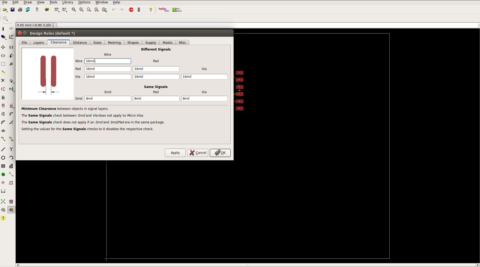
Then pullout all the components into the box and then what we have to make is that edit the design rules.
Clearence is made ok
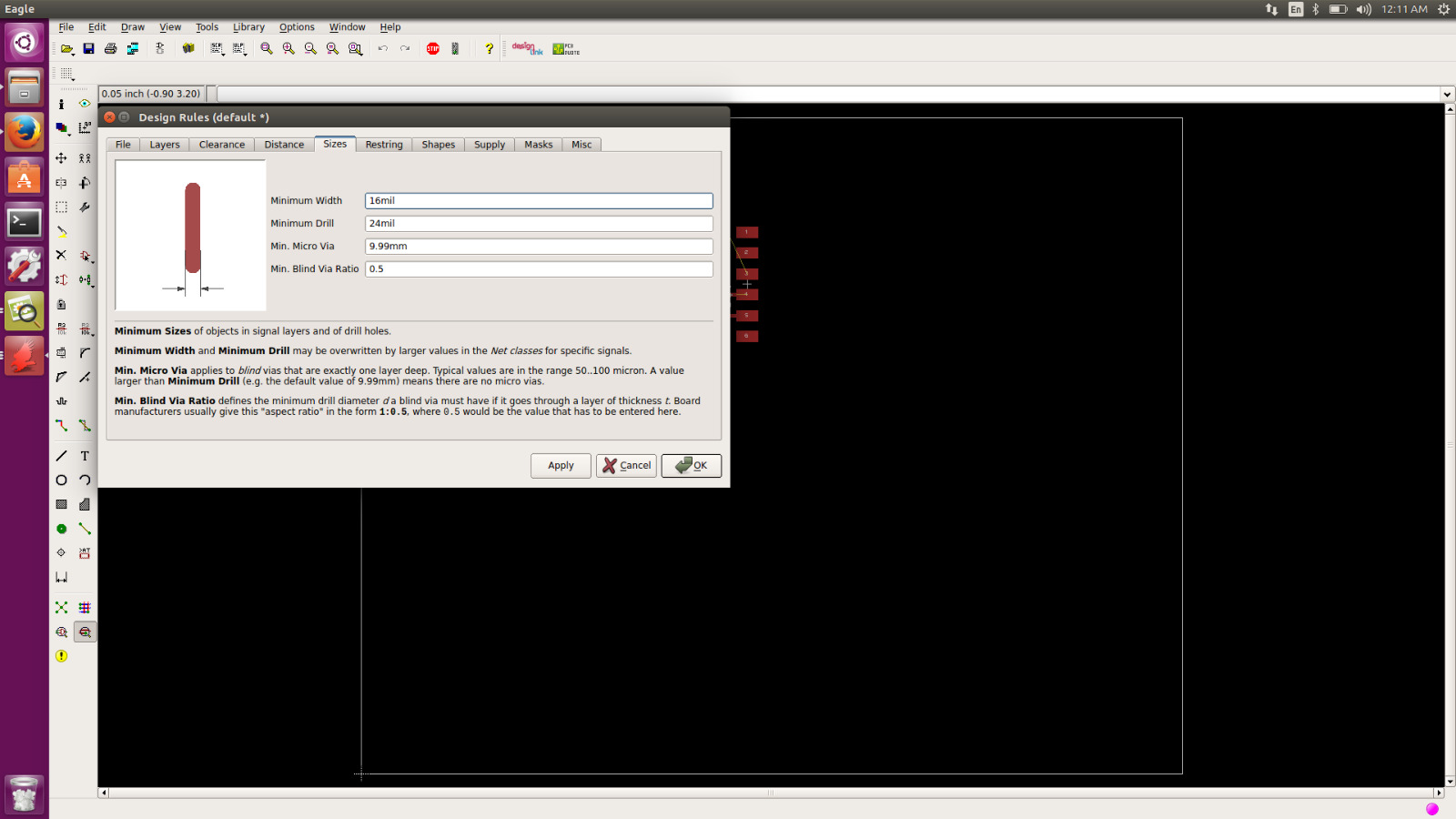
Size is made ok.
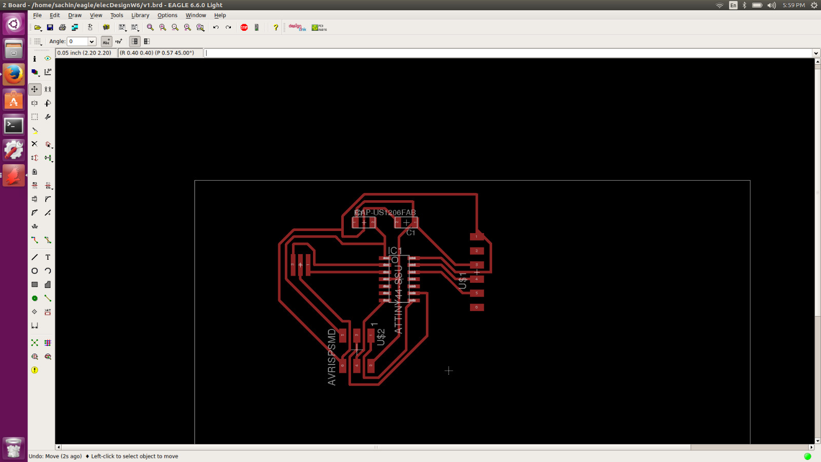
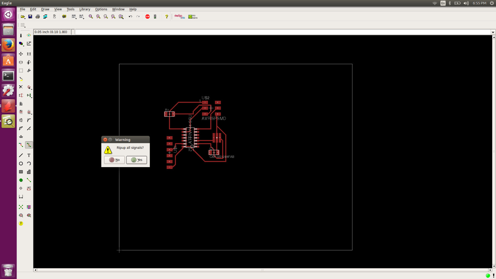
Then auto-route option is selected. One thing that we have to notice is that before auto-routing, since we are printing on only one side, we should select that top layer only and others are made not applicable. While auto-routing if any of the connections can't be auto-routed, then an yellow line is appeared and we we should manually fill up it.
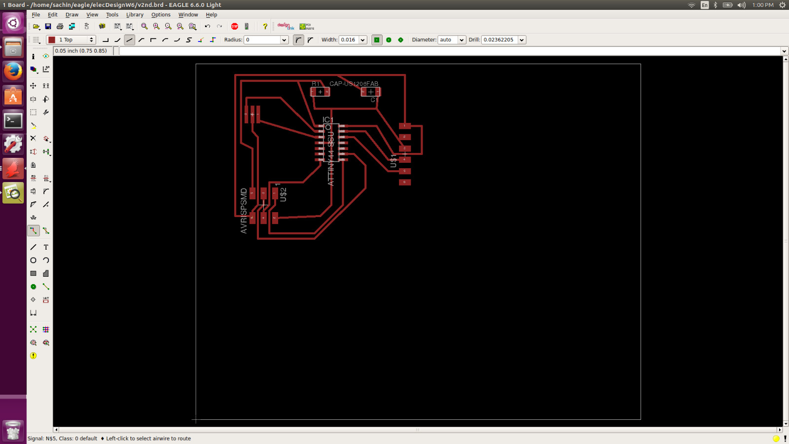
Then we rip-up all the lines to draw it manually. It took some time to draw manually. We can also ripup the selected files only if needed.
Hence I got my hello echo world design without adding any components.
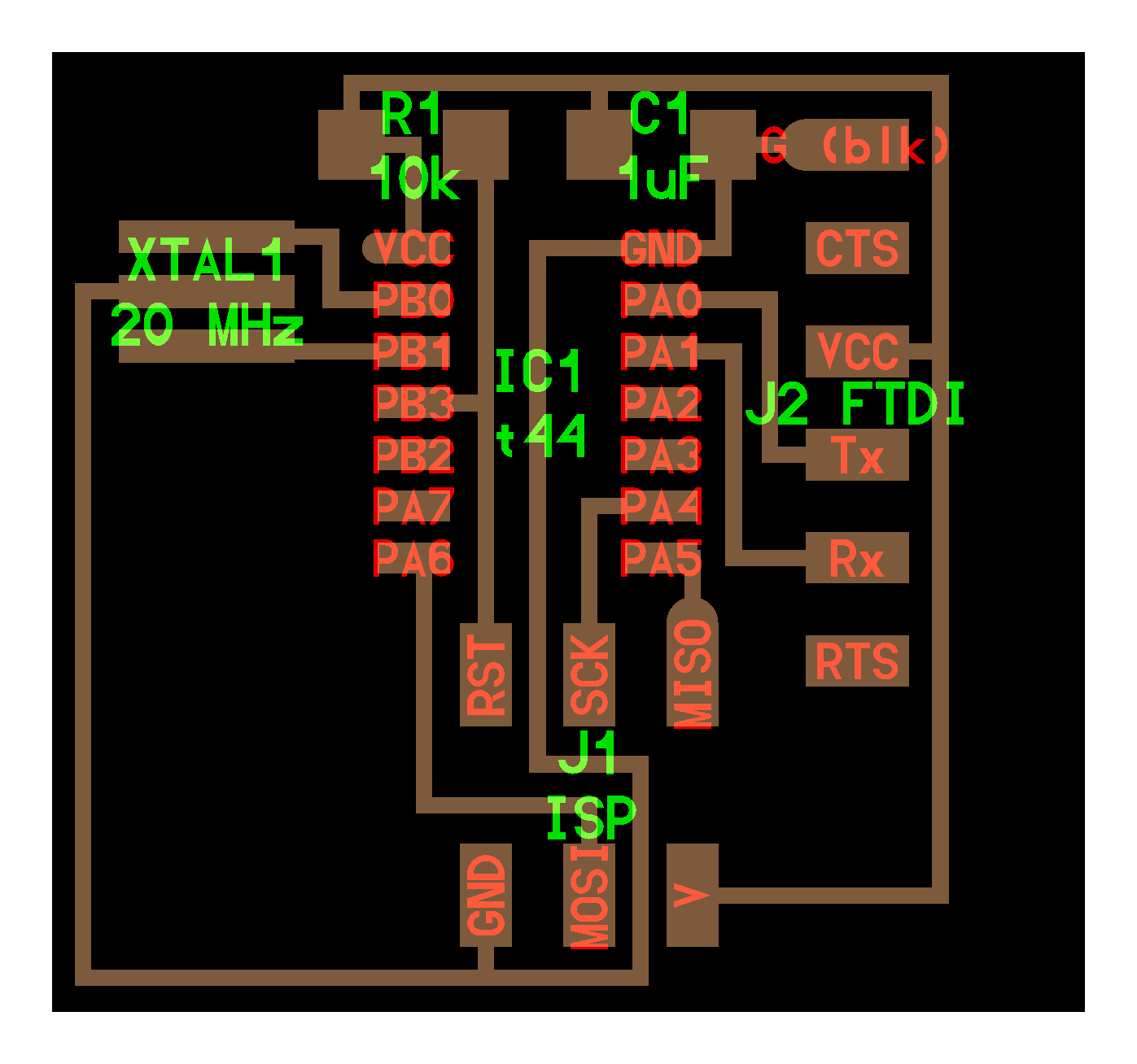
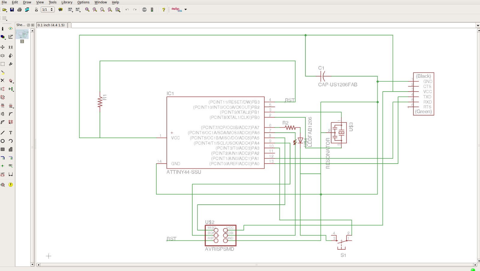
Next we should add one LED and switch. I selected red LED. For the in the design I should add a resistor of 499 ohm.
First I made changes in my schematics
I added LED, resistor and switch to the previous circuit.
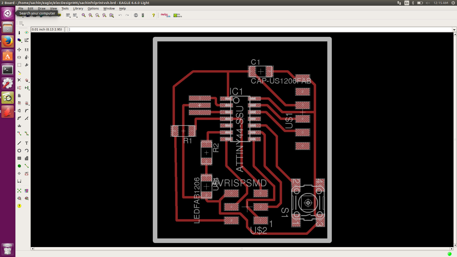
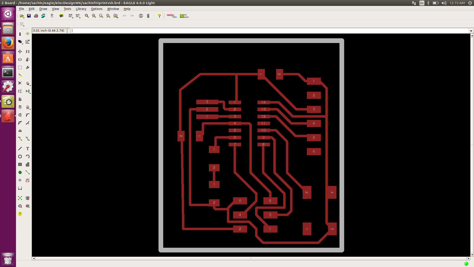
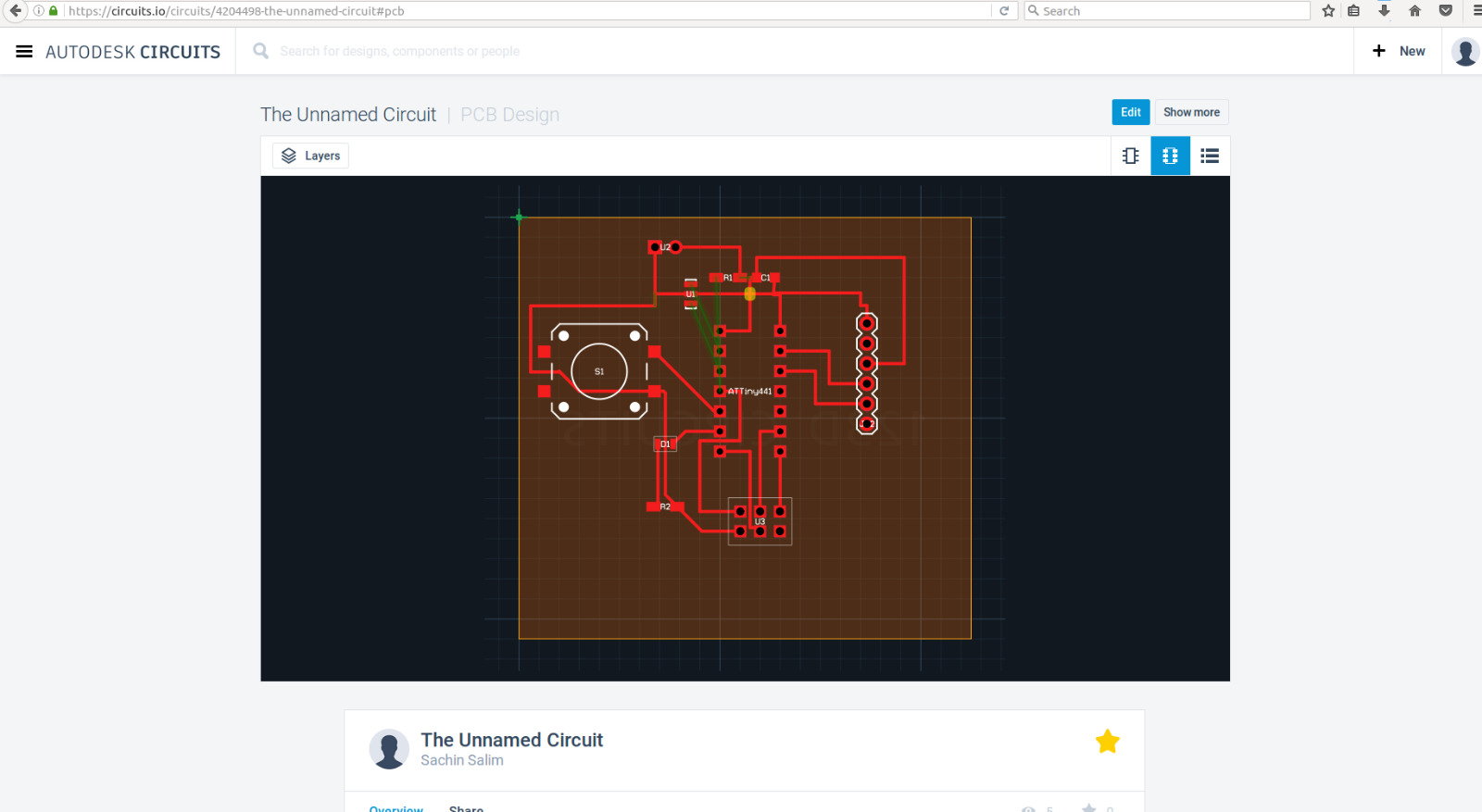
Then I converted it to PCB layout and routed it.
Then deselect all the other listings except dimension and top layer. Then we should get how our board looks like.
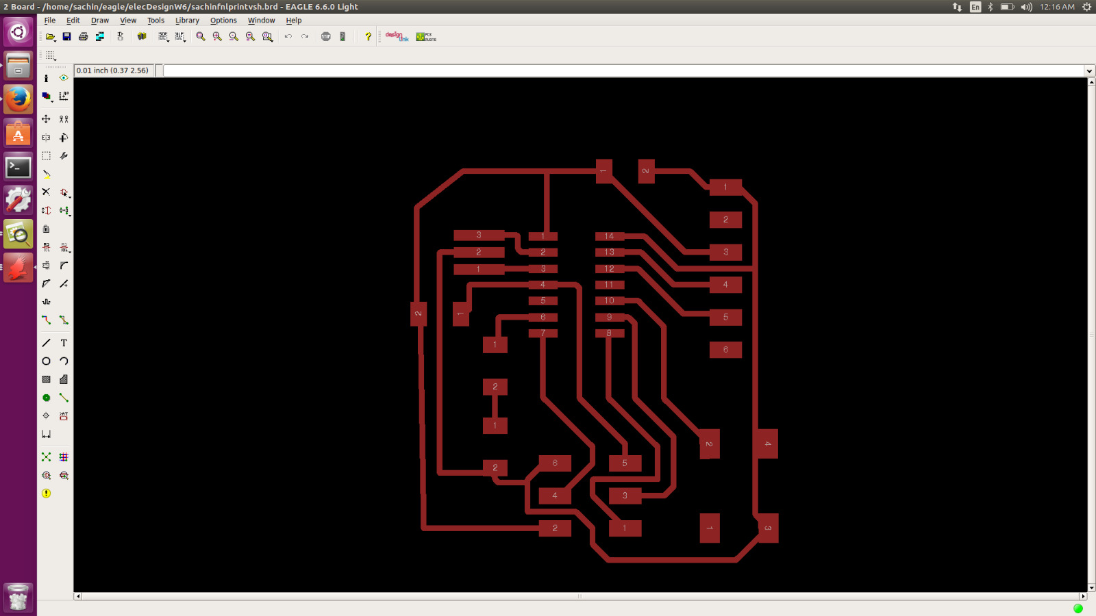
Then select only top that is what is used to mill.
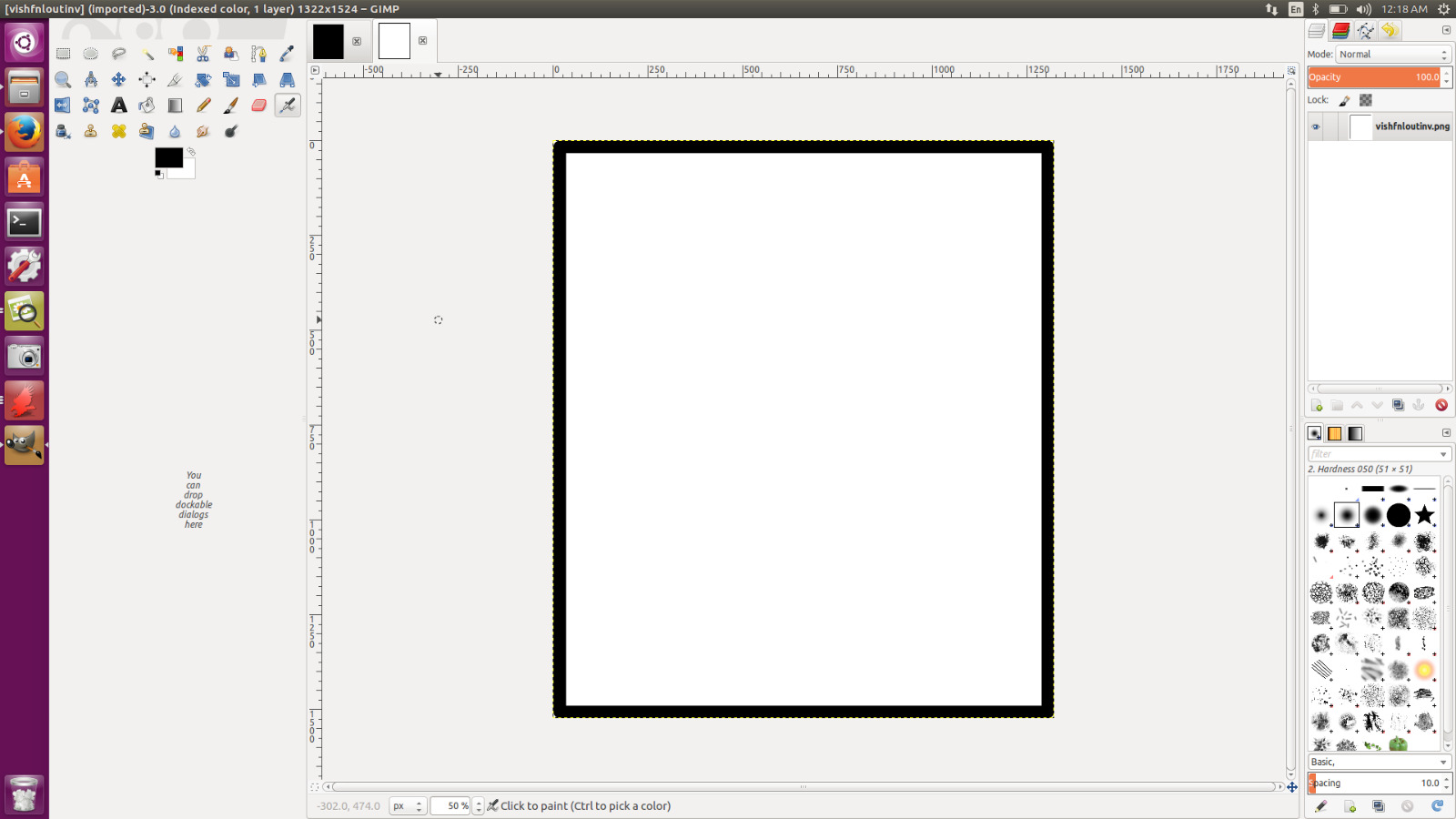
Export it to .png file and select monochrome mode inorder to see in black and white.
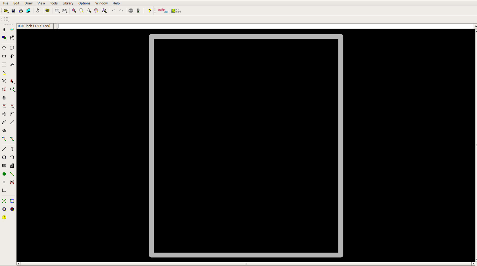
Then select only dimension in PCB Board. Here in properties increase the line width.
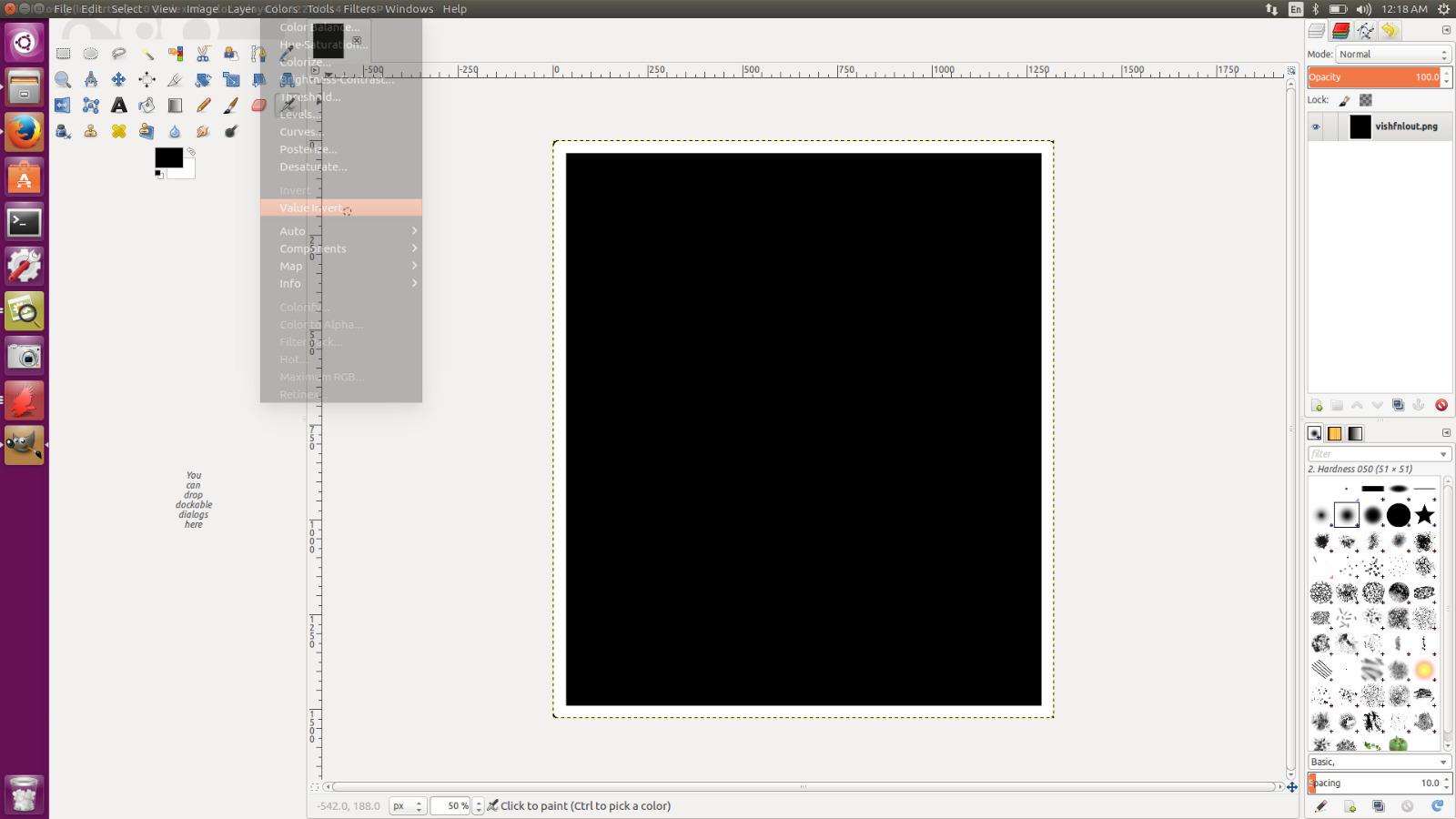
Then export it in .png format and open it in gimp. Invert the colour of the file so that white is that is going to get cut.
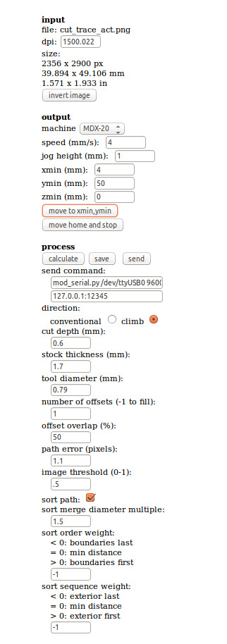
Then next step was that to mill. For that I used fab modules and loaded the image.
After loading both the images as input first of I should mill and then cut as in previous session. Settings I have made here are as follows.
After this I should make path and send it. x and Y should set manually.
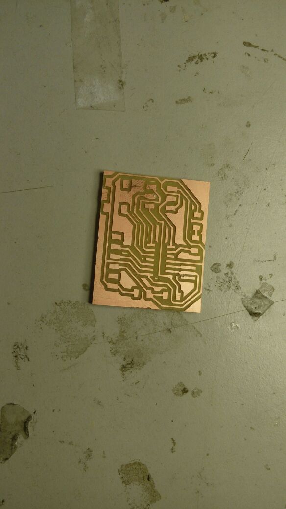
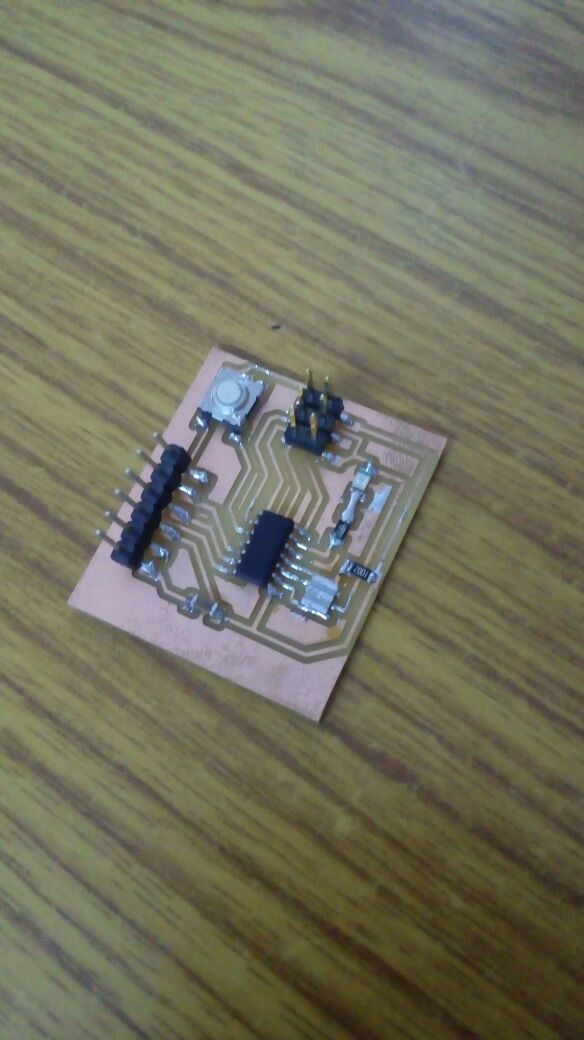
I obtained my board after milling. Now I have to solder the components.
Components needed are:
- Resonator 20 MHz
- Capacitor : 1uF - Resistor : 499K Ohm (RxES 499 OHM 1-4W 1% 1206 SMD)
- Resistors (x2): 10uK Ohm (RES 10.0K OHM 1-4W 1% 1206 SMD)
- ATTINY 44-SSU - AVR ISP
- FTDI-S ( 1X06SMD)
- LED. Blue clear (The negative pole will be oriented to ground)
- Buttom (SWITCH OMRON SWITCH)
We learned how to use the program with an existing board, but for our practice started from scratch, adding components.
Then I started soldering.
Its an online tool. I tried it. As in eagle 1st we have to draw the schematic diagram and then to switch to the PCB layout. Here auoto routing option is not available. After completing the work, we should download the gerber file.