Fab ISP
Week 5, our task is to familiarise with electronic production by the way of fabricating a pre-designed PCB module. Through this we are supposed to familiarise with milling the PCB, stuffing the board by means of soldering and making an in-circuit programmer by milling the PCB
Milling the Board
Roland MDX-20 is the CNC milling machine that we uses in our lab.
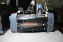
First we fabbers are made familiarisre with the machine. Vishnu, our fab instructer explained us about the machine and how to use the machine in safe and effective way. He also explained about what all we fabbers should get consider for using the machine.
Using this machine, we have to mill our board.
For milling htere are two main things that we need to not down
(i)Mill a circuit board trace image with a 1/64" bit
(ii)Cut out the board outline with a 1/32" bit
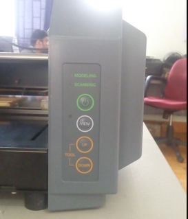
He also have explained us that there are mainly three planes, viz x,y and z. The x and y coordinates can be moved using the control software. The z axis is dependent on how the drill bit is set and needs manual adjustments which can be done using the control panel of the modella itself.
There are two modes
(i)View mode
(ii)Work mode
View mode is where we used to set the desired bit and work mode is that we used to work
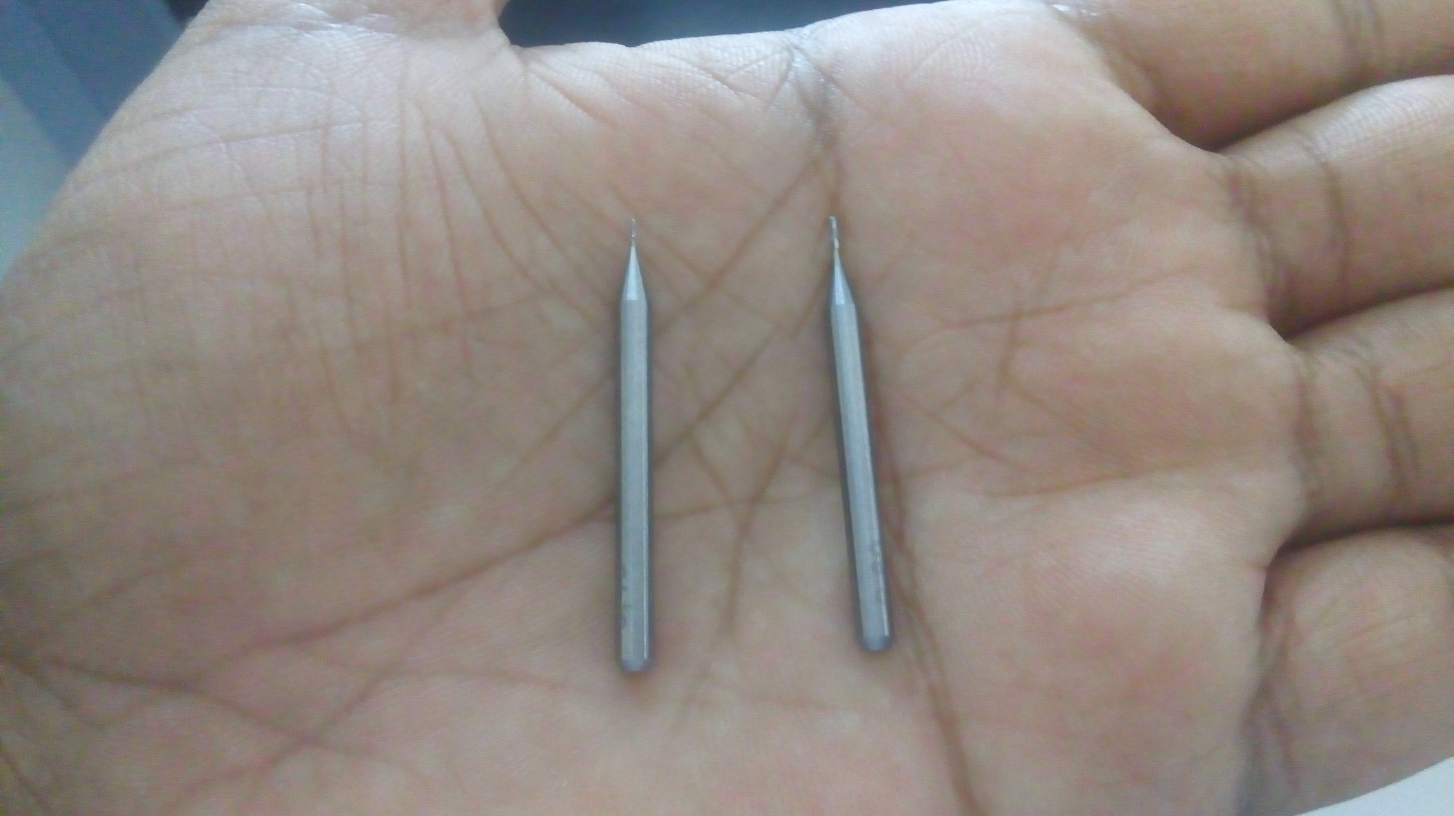
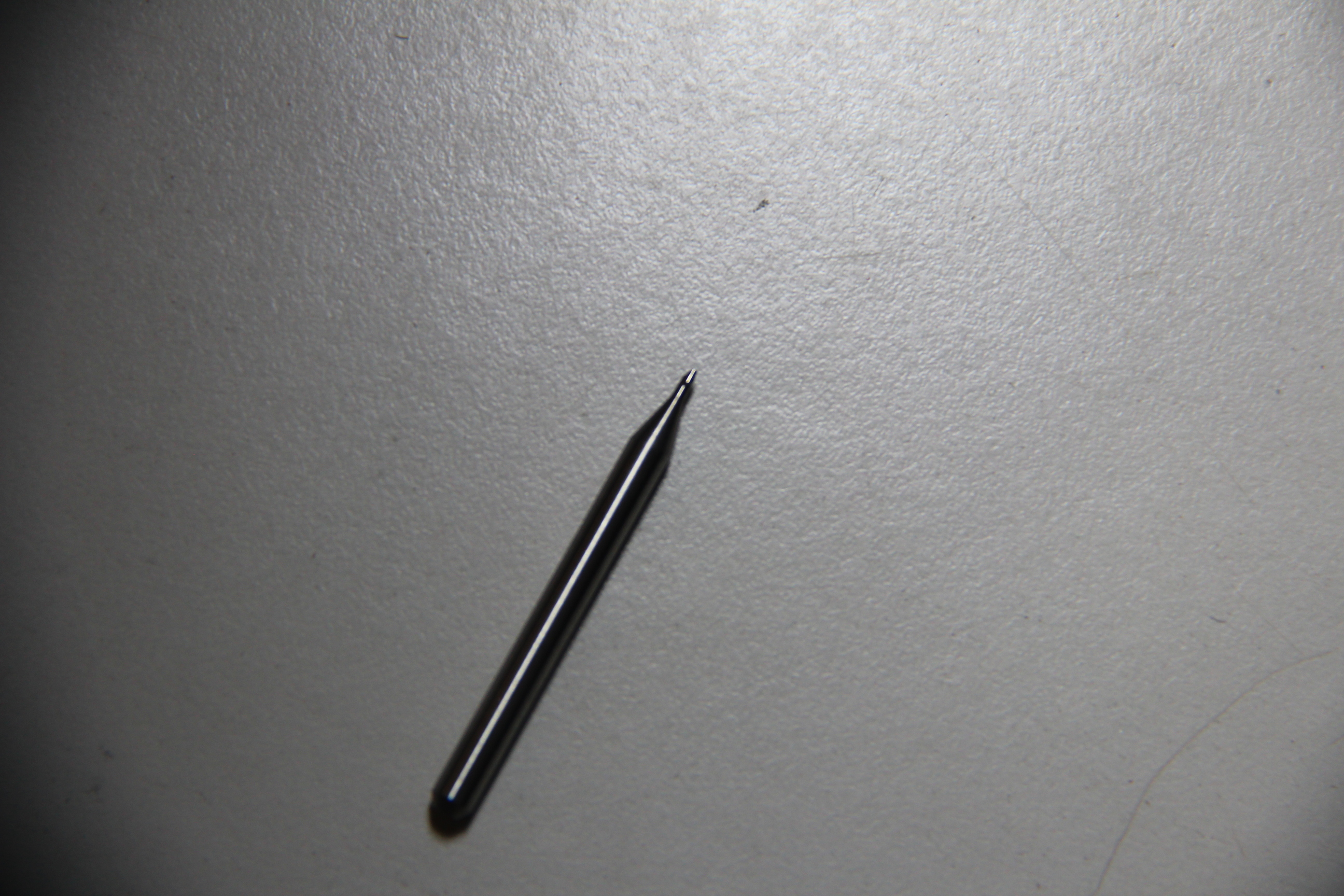
Then Vishnu told about the bits and its settings. The bits are made of material known as carbide and they are so costly. Setting the bit is one another matter that should hold in mind. There is an alenkey by which we uses to tighten the bit. Using that we should tighten the bit from two sides. Then only bit will get tighten. And also keep in mind that it should be kept maximum into the hole and some part of it should be left so that the point of the bit should cut or drill the board properly.
The next was that about mounting PCB
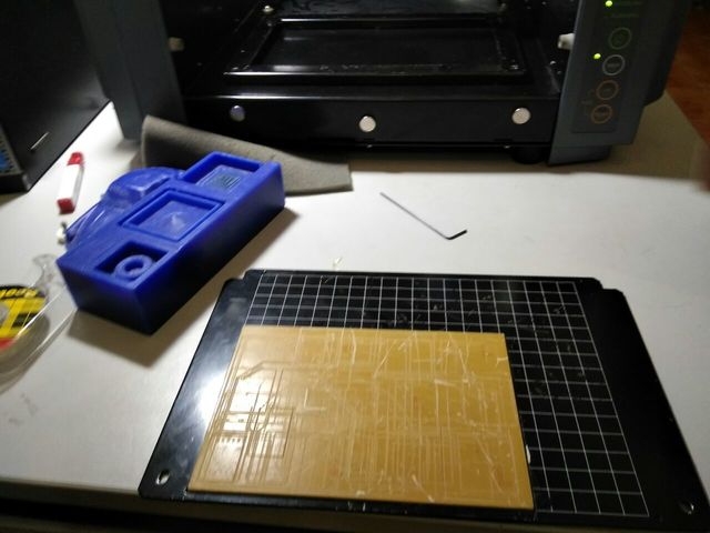
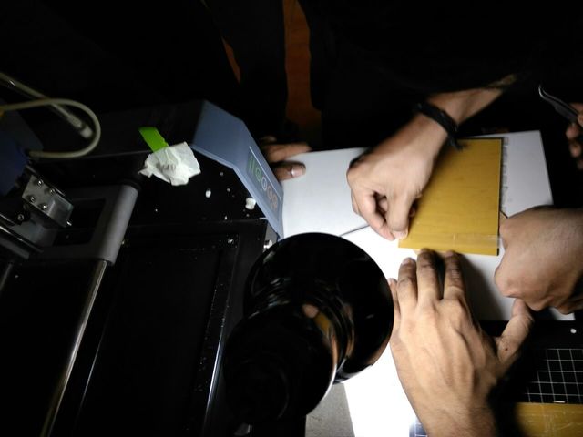
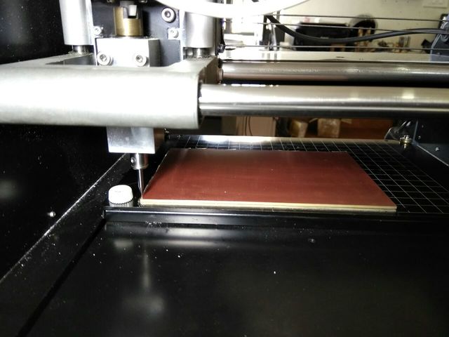
First of all we need to mount a sacrificial layer over the bed. On the top of it, we have to place the board that we have to mill. It should be get noticed that double sided tape is placed in between the sacrificial layer and the board that we have to mill and no uneven or irregularities should be present there. If there are bubbles arises at the time of sticking the tape it also has to be removed.
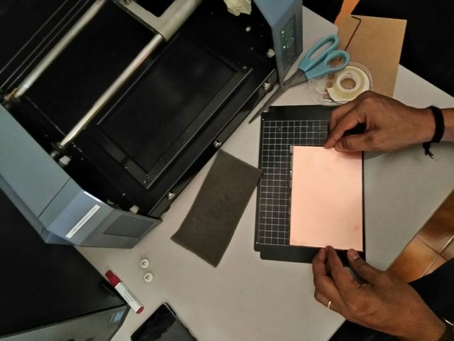
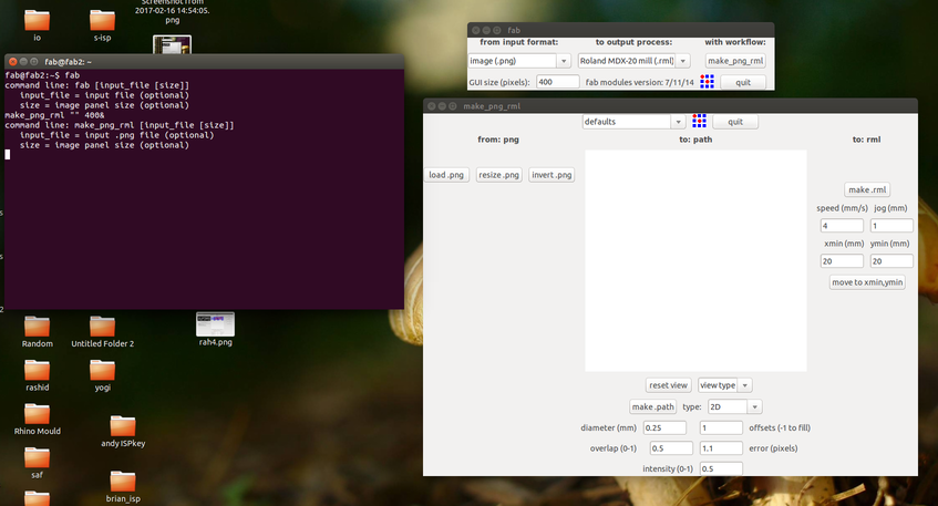
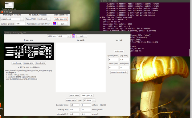
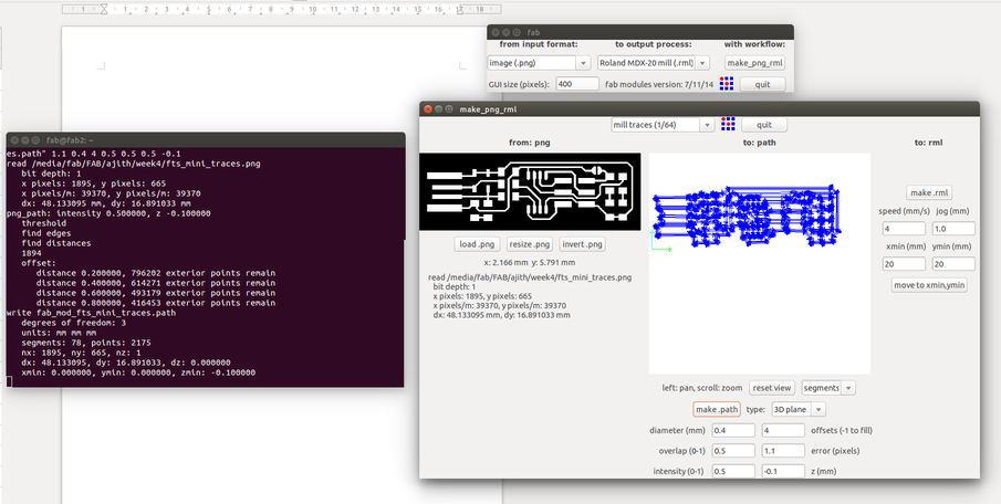
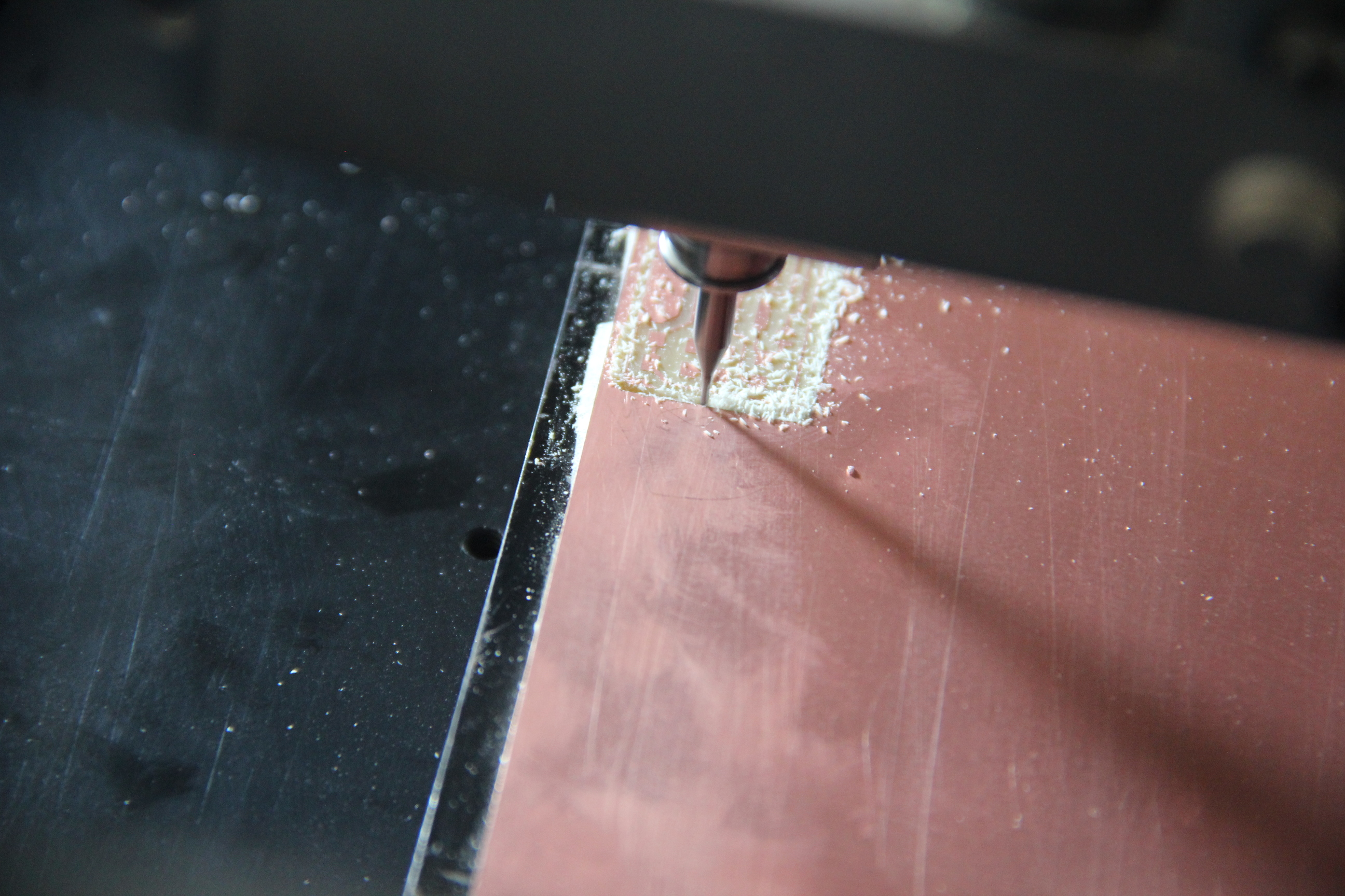
The next is about setting the machine. First of all we need to upload image of the board that we are asked to mill. It should be in .png format. Then next procedure is that the input image is converted to output format. Here the machine for milling is Modella MDX20.Then pcb process have to be selected. If it is milling, it should be PCB traces(1/64) and if it is to cut it should be PCB outline (1/32). Then we should make path. We can see the make path. Then settings should be changed if necessary. Here we left it as default. Then make.rml and send rml.
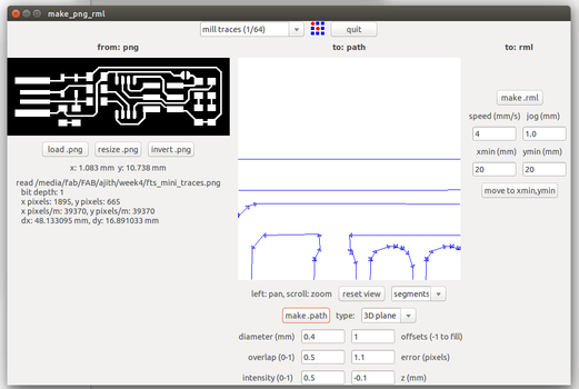
Now the next step is to set the origin, for which the x and y positions are set using the Modules control software. Btw, we can move the milling head only in modella's view mode. Once the x and y positions are set, the z position is to be set. For that the drill bit is to be fastened manually, such that it just touches the copper surface or move the drill head using the control panel of the modela to do the same. Now that the origin point has been set, we can proceed to mill by 'make send' in the control software before which me move out from view mode.
For cut the other bit is chosen and set its origin as that before as mill. Settings and all are as such as before.
Removing and securing the end mills is the next process that we should get conssider. It should be removed and secured in a most delicate and precise way so that nothing should happen to the bit.
After the work, the bed should be get cleared by using the vacuum cleaner provided
Next Yadhu, our other instructor showed us a demo on how a PCB can be milled.
FabTinyISp
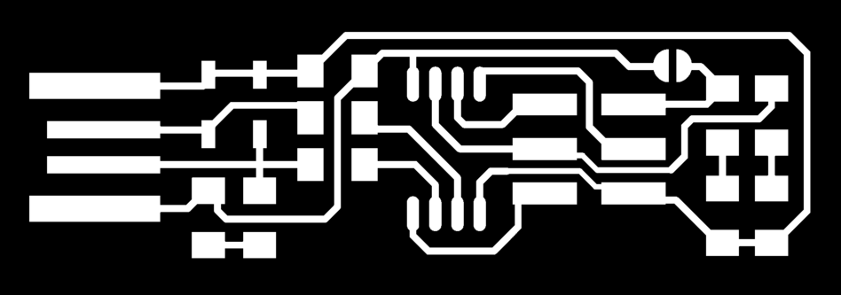
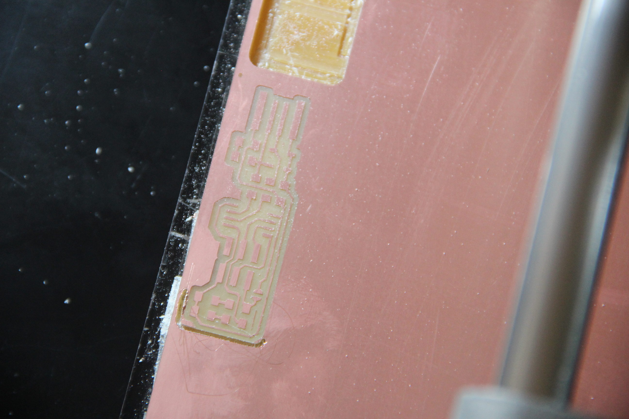
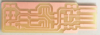
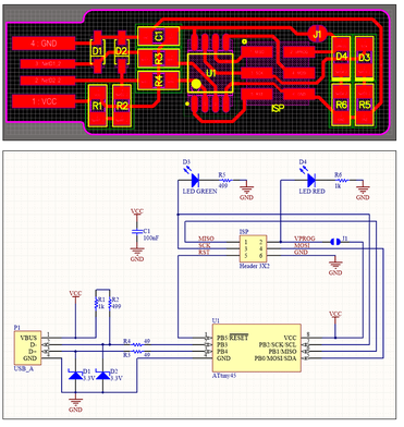
I chose ATtiny45 board. Its much simpler than other boards. I went through the schematic diagram and position diagram. Then I went through milling traces and cut layout. I downloaded the layouts.

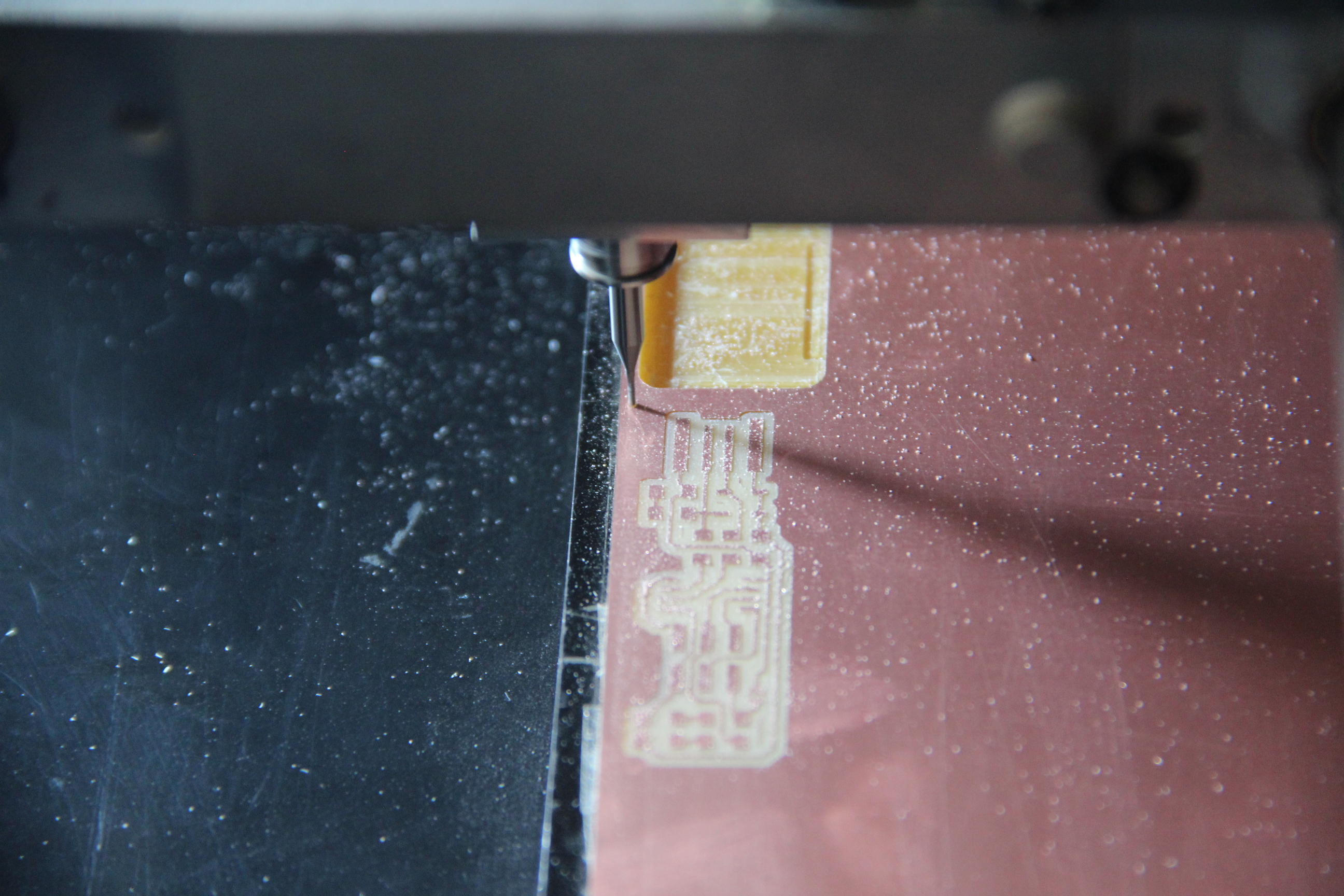
As per above I adjusted settings over the UI. Then I adjusted the x axis as 50 and y as 0. Then I fix the bit to drill. I actually milled in a fine manner. After milling what is happened is that I replaced the bit with 1/64 to cot the board. Then after all the above settings, what is happened is that cut started and at once the bit has broked. Atonce I stopped the machine and removed the bit. I entered that on log and adopted another bit.
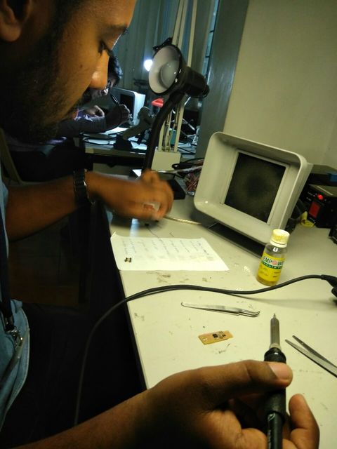
Soldering the board
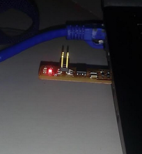
The next is that to solder the board. For soldering I first of all note down the components required to solder from the schematic diagram. Then corresponding to each component name, I pasted a double sided tape so that each component can be placed in a better manner.
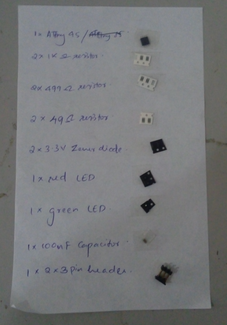
Here while soldering the polarity of diodes and IC have to be noted.
Put some extra solder in USB connected parts.
Before soldering process starts switch on the filter.
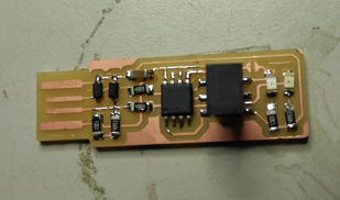
After soldering, continuity should be checked so that to ensure all the connections are made properly.
Programming Fab ISP
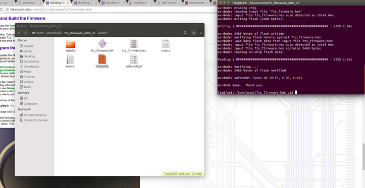
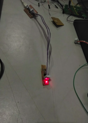
Here I followed Brians documentation. As per the instructions given, I installed avr dude and downloaded the source code files. After software installation and building the firmware the next step is that to program ATiny45. Then update MakeFile. Here open the make file in the directory in gedit and near the top find the line saying "PROGRAMMER ?= usbtiny" and change usbtiny yo the programmer you are using. I am using a ATtiny board so no need to change this. Test by connecting to usb. Now we can connect the device to a usb port and see if the red led glows. Connect the programmer to isp headers of the board. Erase target chip now erase the target chip by typing make flash. Then on configuring the fuses run. Make fuses to configure. Blow the reset fuse run rstdisbl(reset disable). Disconnect the jumber and now remove the connection we extablished befor programing.