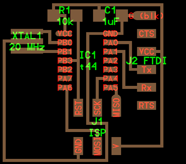
This week assignment was to make a Hello EcHo Board. The board diagram is already given we want to redraw it with LED with a current limiting Resistor and switch so additionally we want draw and mill the given circuit with these components. The board is already with Microcontroller (Attiny44), osscillator ,capacitor and a pull-up Resistor (pull-up Resistors is used to ensure the wire is pulled to a high logical level with the absence of input signal).

GROUP ASSIGNMENT
Here in group assignment we want to check the operation of microcontroller circuit board by using the equipment in our lab. Here in our lab we have
multimeter
Digital Storage Oscilloscope (EZ Digital DS-1100 100MHz)
Function Generator (25MHZ AFG 2125)
Multimeter
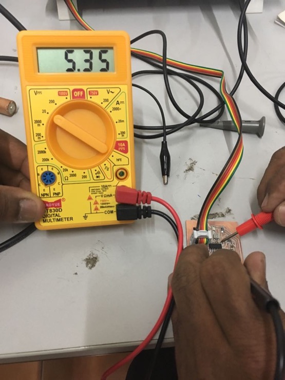
Using multimeter I checked the circuit conductivity ,here I checked the voltage across ATtiny 44 and I got the voltage as 5V
Digital Storage Oscilloscope (EZ Digital DS-1100 100MHz)
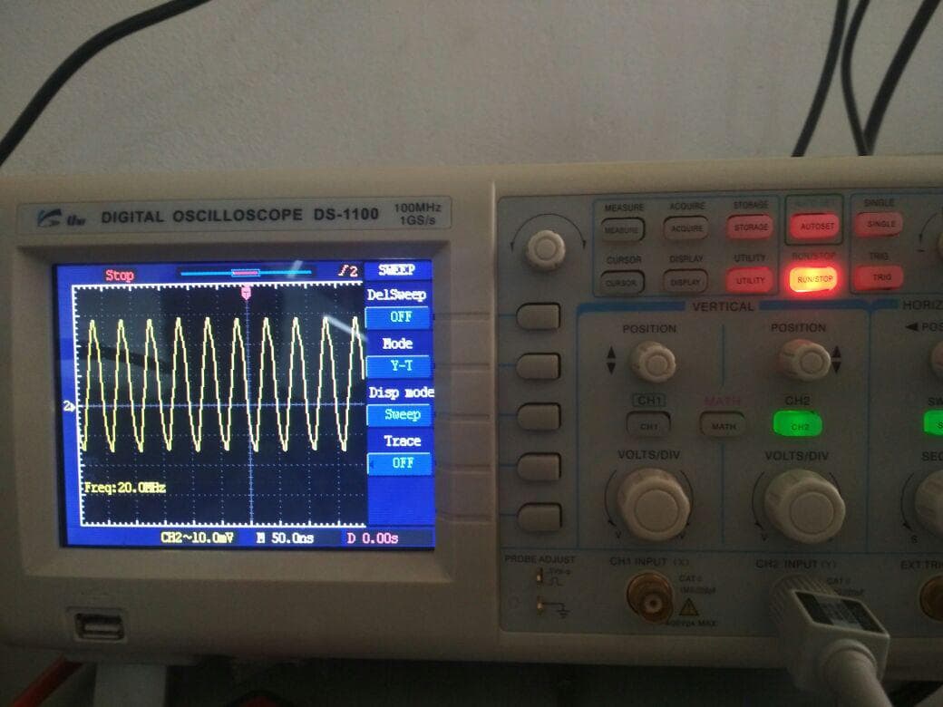
Here we used oscilloscope for checking the frequency generated by the Resonator . we get 20mhz as the frequency .
Function Generator (25MHZ AFG 2125)
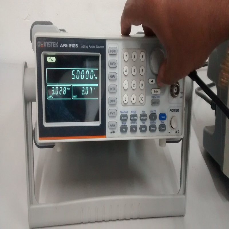
For giving signals to the board ,function generator is used to check or calibrate the graph on oscilloscope .We set the oscilloscope at 50ns for attain a clear spectrum
PCB Design Software
There are somany PCB design softwares but I used EAGLE (Easily Applicable Graphical Layout Editor) Software to creat my PCB borad. This software was easy to use and it is the software that widely using by the people for PCB design.
Using Of EAGLE software
EAGLE software is developed by AUTODESK so for installation we need to create an account in AUTODESK then we can install it easly, after installing the EAGLE you need to add "Fablibrary" to the Eagle.

FAB LIBRARY
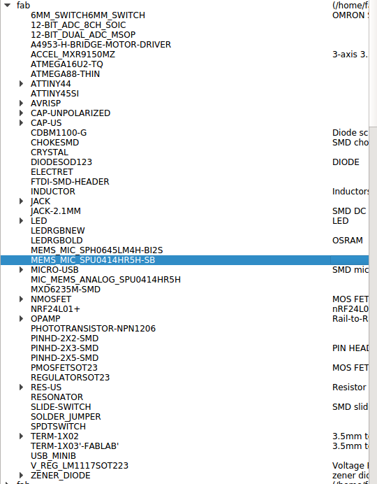
Fab library is the collection of all components available in the fablab . So here we can select the avilable components for our design , After adding the available components you can start drawing your schematic diagram
Making of schematic diagram Using tools
Add:- Here we can add components that we want to make our board
Move:- Move tool helps to take the exact position of component that we want (movig of
components)
Rotate:- Here we can rotate our components in afixed point
Root:- Root is the tool that gives the path of circuits here we can give the connenction between
the components manually
Here we are drawing the given HELLO ECHO BOARD with additonal LED, Resistor and Switch so here the components are using for drawing the diagram
ATtiny 44-ssu:- datasheet
20mhz Resonator : for giving frequency accurate and fast
6mm switch omrom
AVR ISP SMD HEADER:-for programming the board
FTDI SMD HEADER:- powers the board and allows it to speak to the computer
10k resistor
1 mF capacitor
GND
VCC:-power supply
RED clear LED with 499ohm resistor
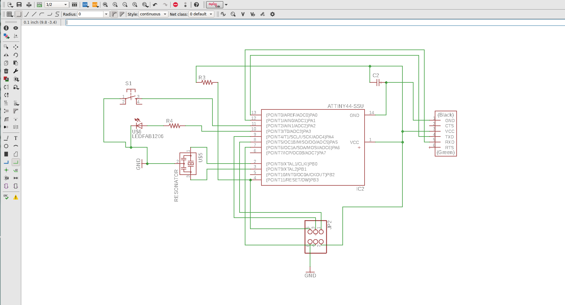
After drawing the schematic diagram by reffering the Given Echo board design ,I changed it into board diagram by file < switch to board then gave the "clearence and size of the trace "
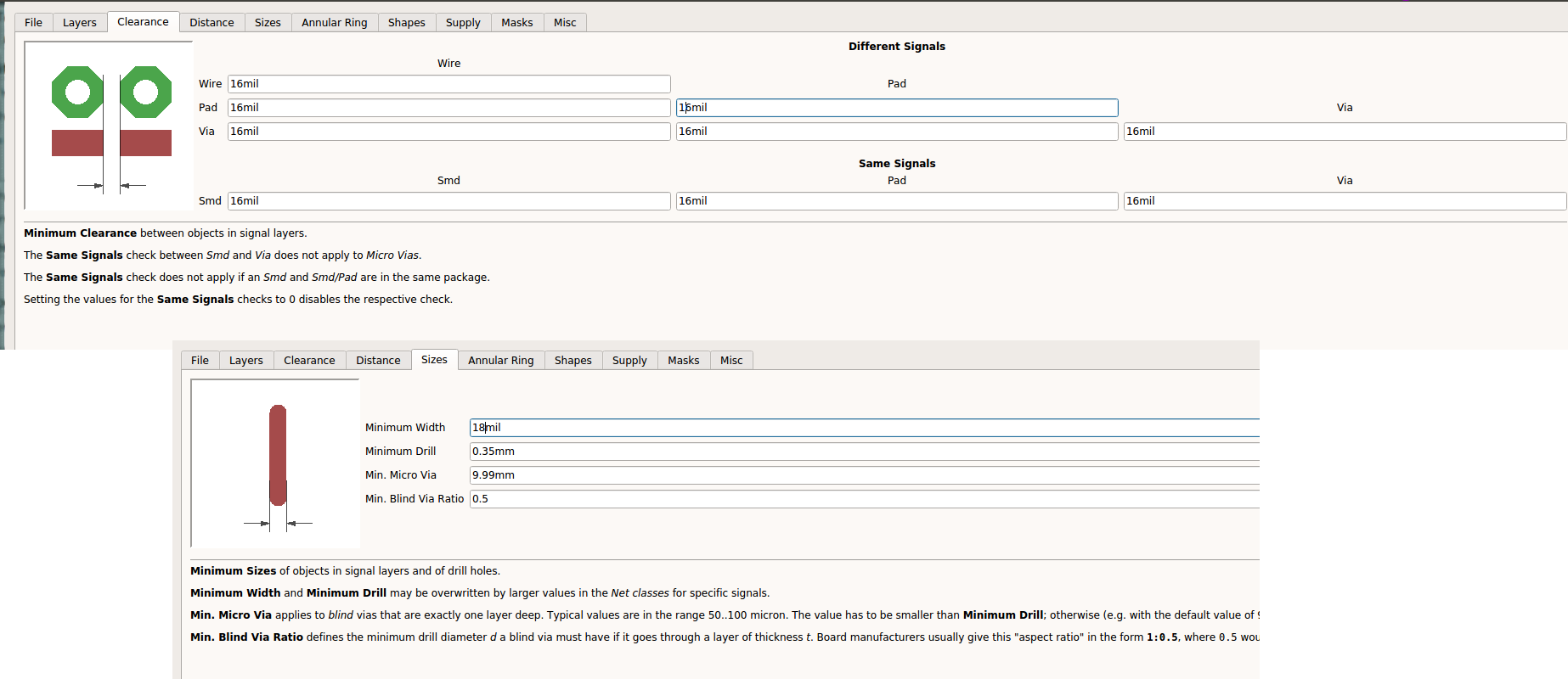
After giving the clearence and size of the trace gave the automaticrout in tool < Autorouter then i got a clear 100% route
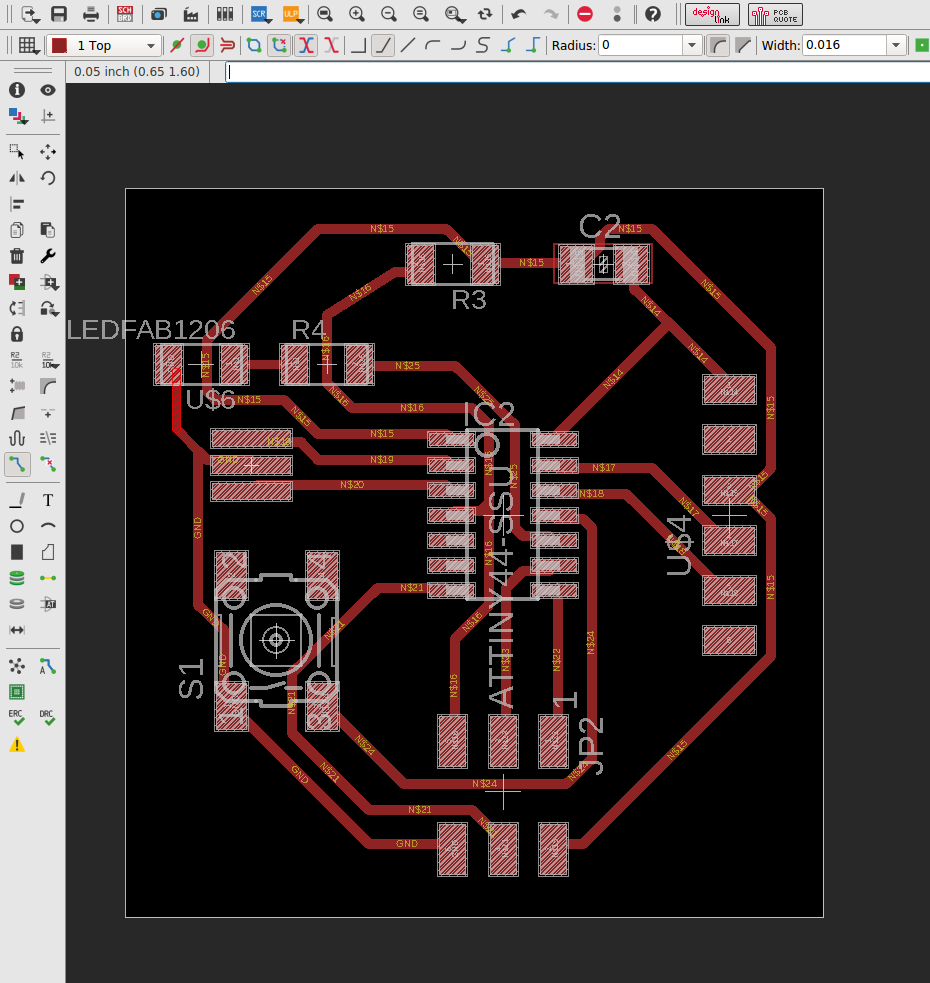
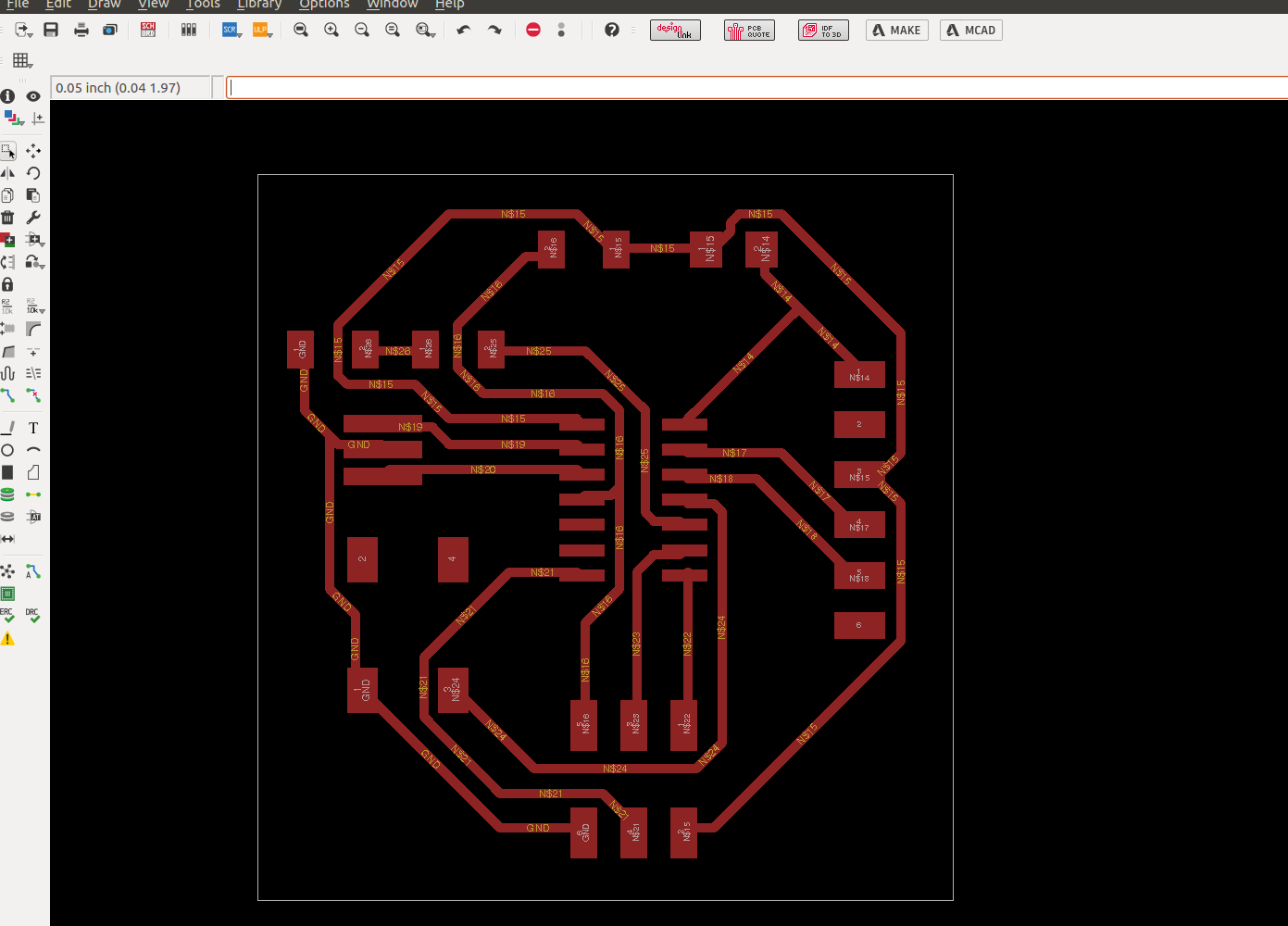
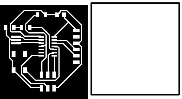 .png images for mill and cut
MILLING OF THE BOARD
For milling we have to change our board into .png file selected as monochorme and gave the resolution. After changing into .png we can open it in fab module here for milling and cutting of my board. I used Roland modela(MDX-20) for milling in our lab ,fab module is the print manager using in this machine. Here 1/64 bit used for the trace and 1/32 bit is used for the cut.
After open the .png image on the fab module set the "xyz" origin the give print .
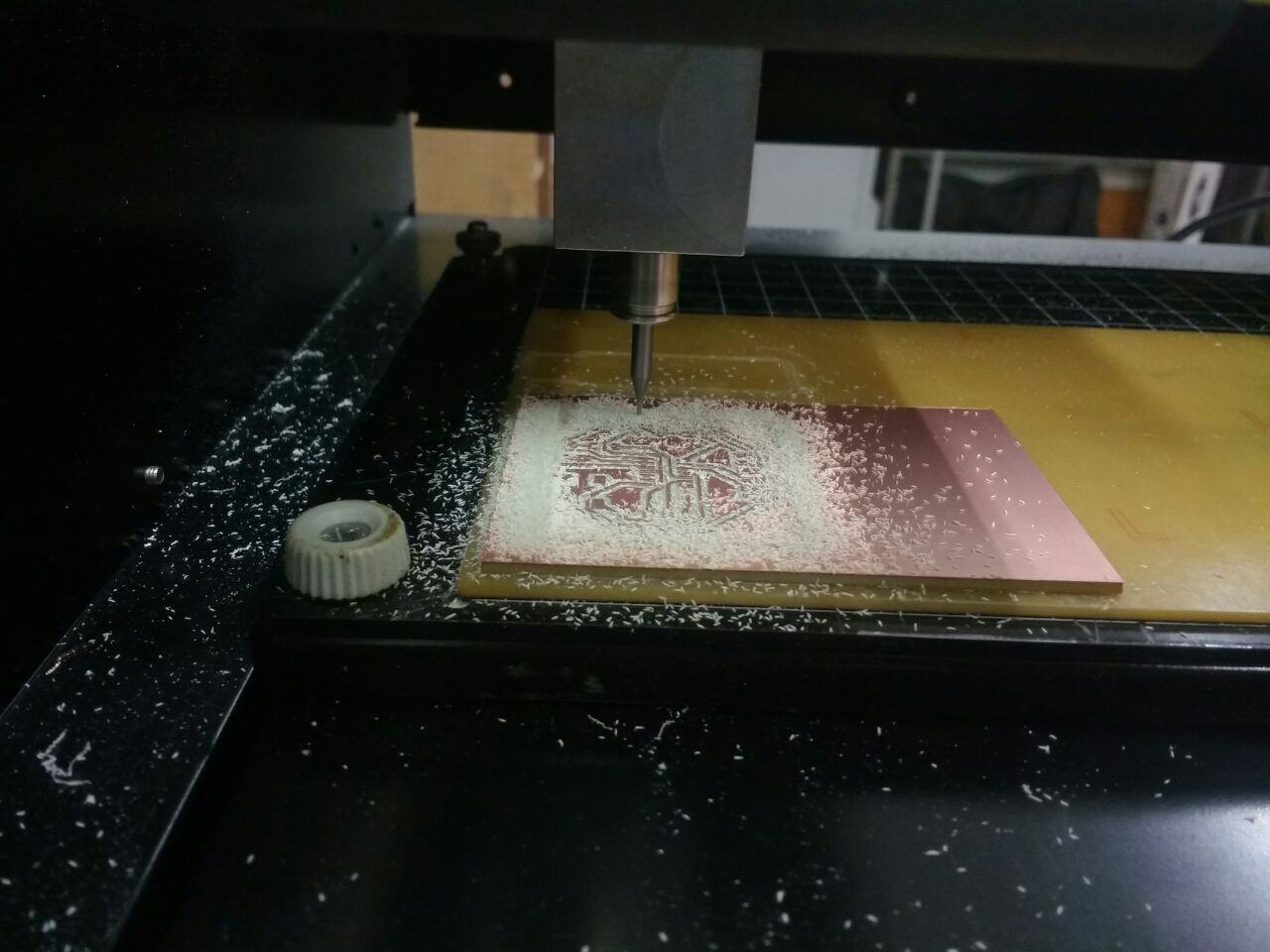 tracing and cutting of board
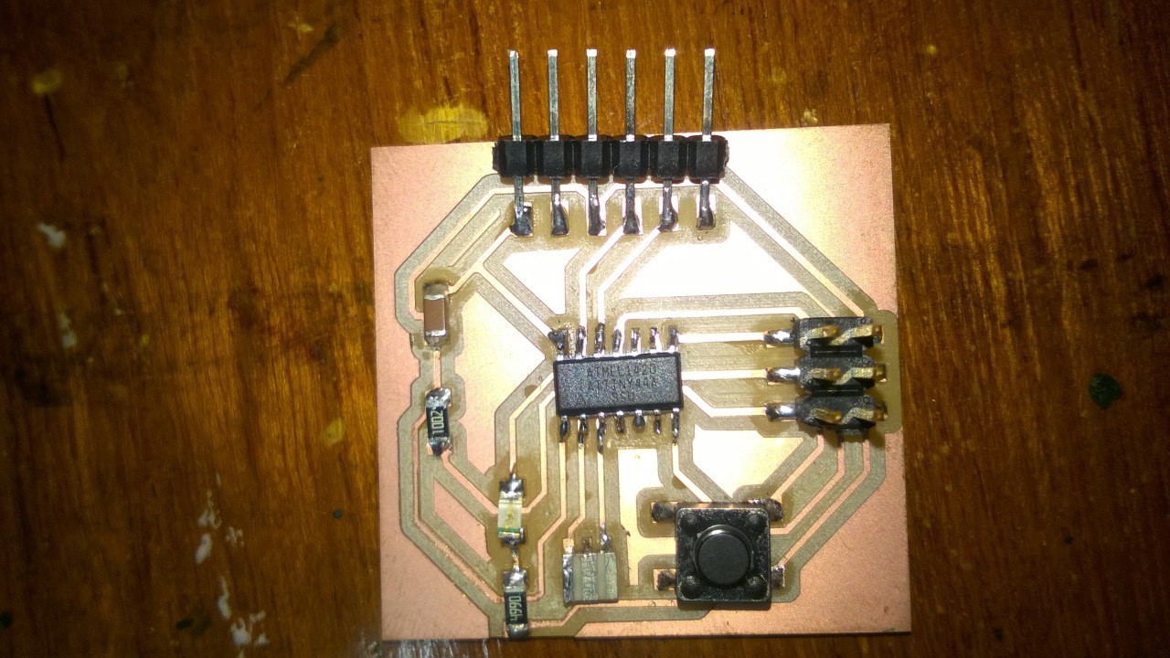
 Board after milling
soldering of the components
I think the soldering is pretty much easier than last time . I picked all components like a list for arranging the components with avoiding the mistake .The components I solderd are;
ATtiny 44
20mhz Resonator
6mm switch omrom
AVR ISP SMD HEADER
FTDI SMD HEADER
10k resistor
1 mF capacitor
RED clear LED with 499ohm resistor
After soldering I checked my board with multimeter either there is any mistake in my soldering or board
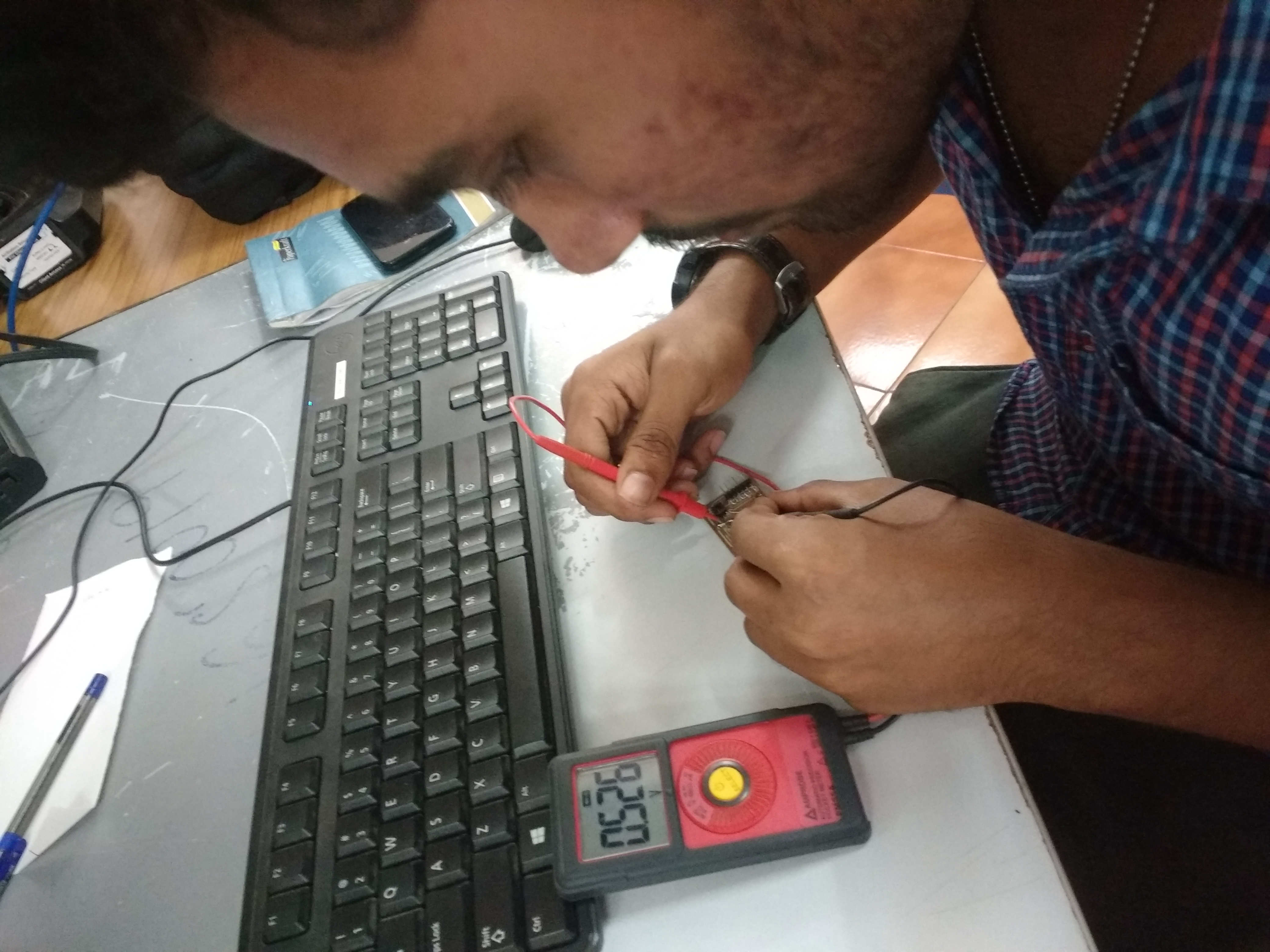
ERROR OCCURRED AND SOLVED
Here I got a mistake with my board diagramme , when I draw the schematic diagram instead of connecting the ground in all circuits I gave GND symbol thinking that it will automatically route all the GND ,So here I put a ''JUMPER'' for connecting all the GND as one
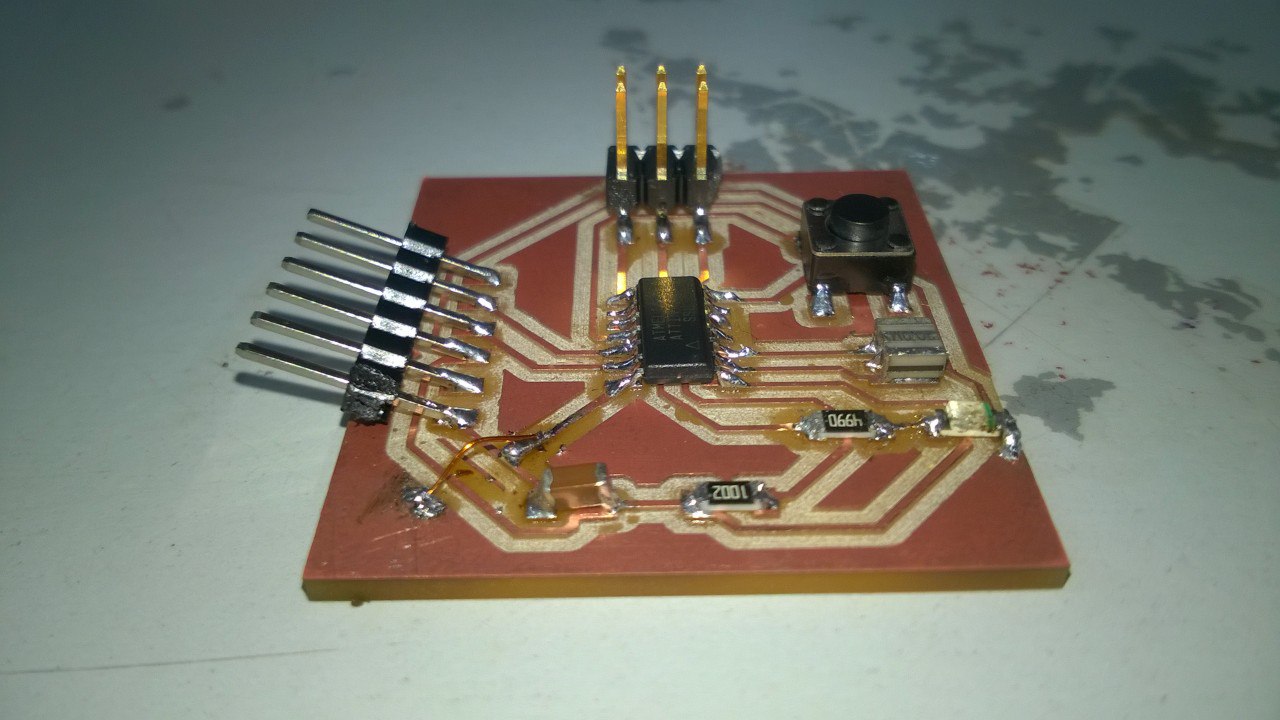
Here I got the idea either I gave a wrong GND symbol or it is not the right way .Give the root manually will give the right circuit with complete connection.
PROGRAMMING OF THE BOARD
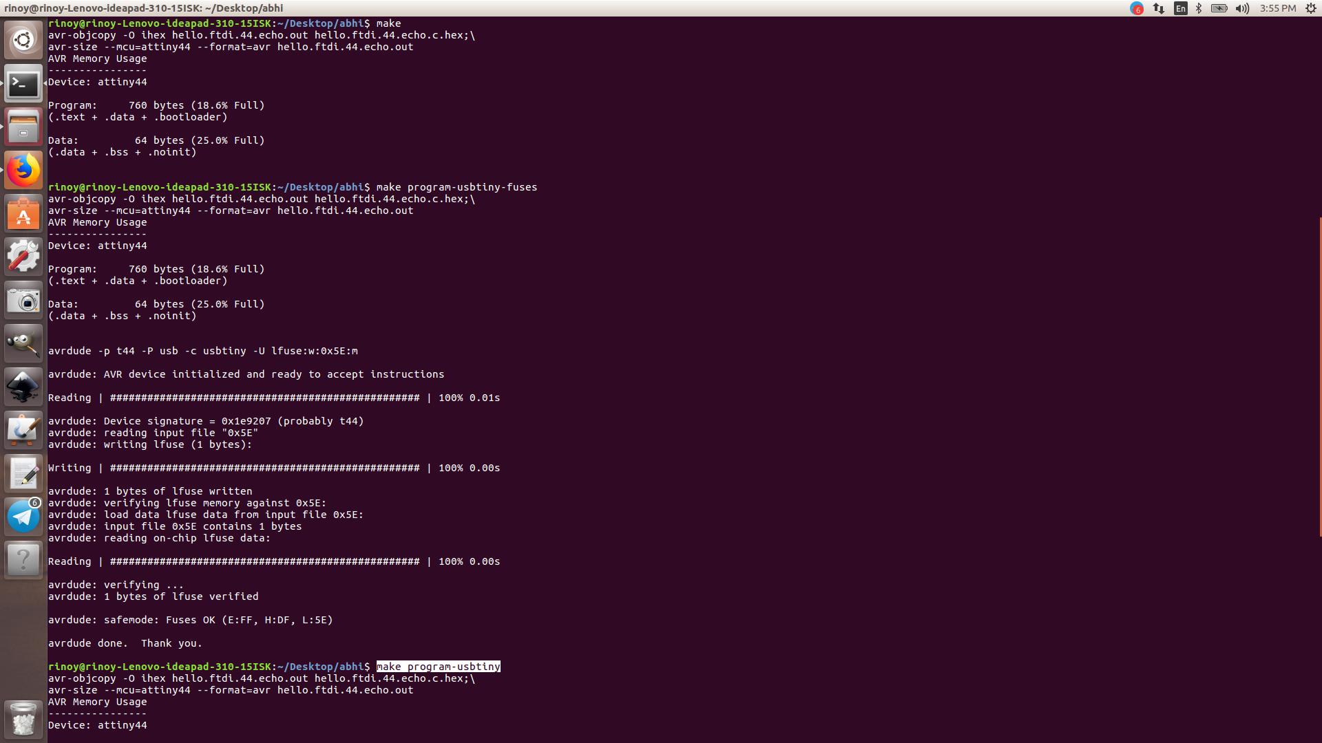
I want to programme my board working as per the echo hello world programmer .So I downloaded .c file and .make file from the schedule of fab academy then,
Renamed .makefile to "Make file"
opened the Terminal and added these below commands
make


make program-usbtiny-fuse


make program-usbtiny
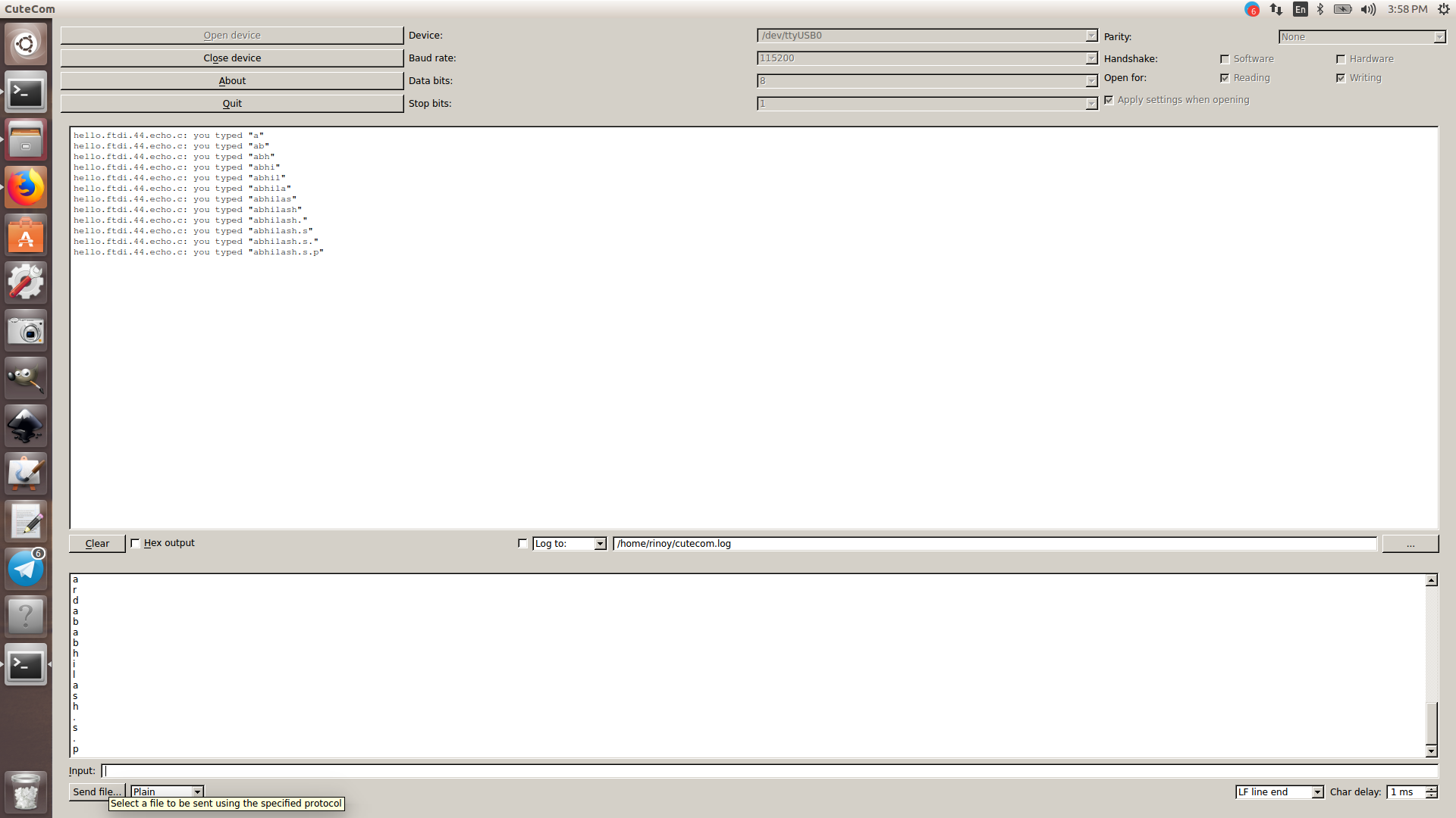
Then downloaded cutecom for checking the working of my board by using the command in the terminal"sudo apt -get install cutecom" after that i checked my board using my name and it echoed.
.SCH file you can download here
.BRD file you can download here
Trace.png image can download here
Cut.png image can download here