1.PCB MILLING
In this week's assignment was "How we can make a printed circuit bord (PCB)".The week was very intresting with milling,soldering and programming of the device that we have made also "CHARACTERIZE THE SPECIFICATIONS OF PCB PRODUCTION PROCESS".PCB bord is mainly made with copper sheet here we can fix our electrical components. We have FR-1 PCB bord for milling purpose it have two layers the first one is a thin layer of copper sheet and the second one is moulded hard paper layer so beginners can easly do that.
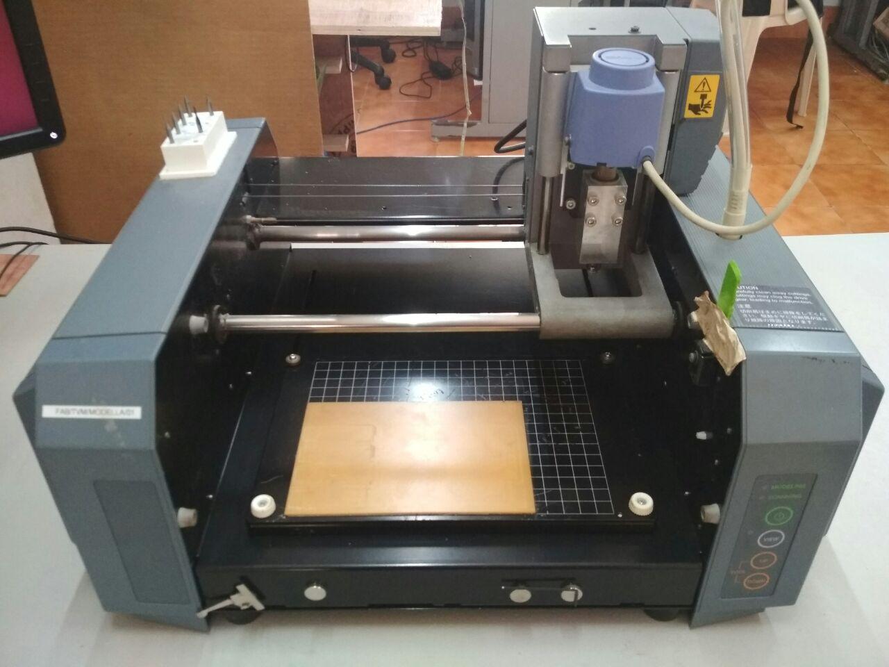
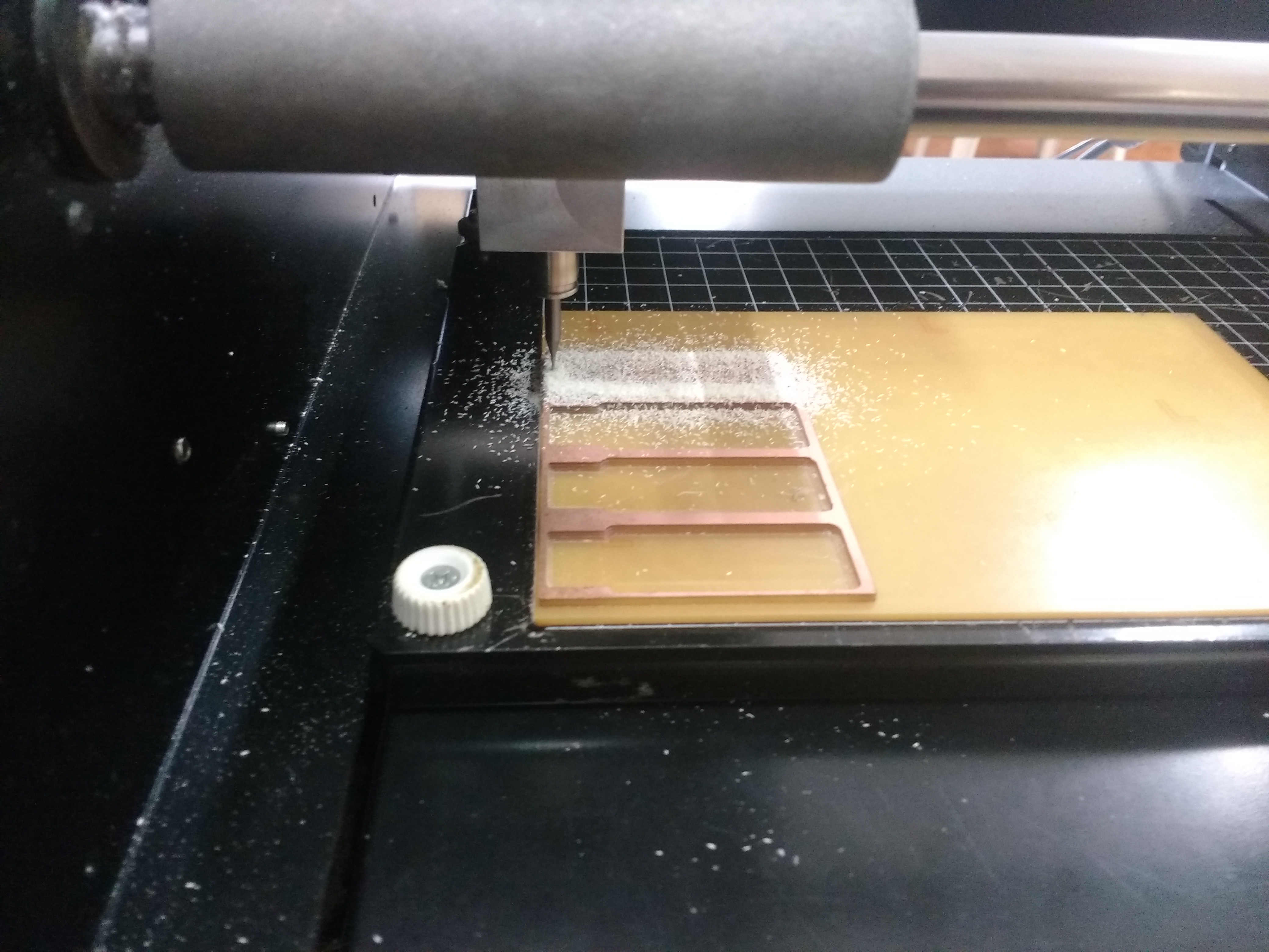
We use the Modella MDX 20 to machine our PCB. It has a tool head travells in x-direction and the bed in y- direction also has a bit whit moves in z-direction which helps in the milling and also cutting process
2.GROUP ASSIGNMENT
The group assignment was "CHARACTERIZING THE SPECIFICATION OF OUR PCB PRODUCTION". The Modella MDX 20 machine having the head with a CNC arrangement so the bit can mill and cut the bord through accessing of "fabmodule".
MAIN KEYS IN THE MACHINES
POWER BUTTON : for switching on and of
VEIW : the view button can use for view the state of milling or cutting at any state of cutting after veiwing it will restart the process at that place
UP & DOWN : for shifting the head up and down to set origin manually
GRAVITY SETTINGS
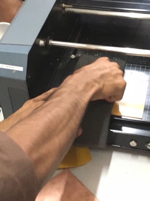
Here the bit want to tight manually on MDX 20 machine so we want to set it carefully because the bit can get easly damage
So we need to lie a sopnge above the bed taking as a precaution for avoiding the braking of the bit.
CHARECTERIZING
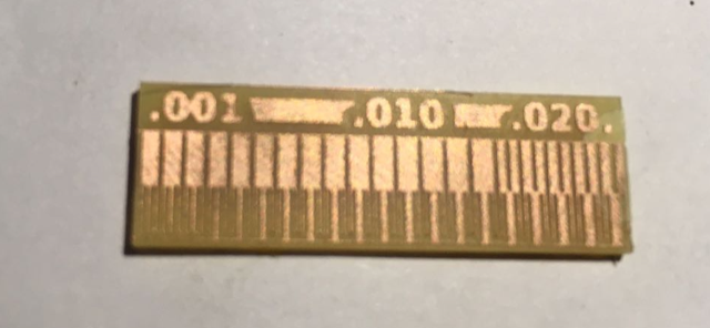
To find the "TRACE"of our machine download image from fabacademy's this week page
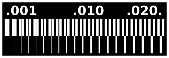
Here we got the 1/64 inch bit can trace the thickness of 0.001 and 0.01.also we got the idea of milling with this machine there is no playing from the machine when we cut our pcb bord it give a clear cut .Here the trace width less than 0.4mm came out imperfectlly
3.MY EXPERIMENT
I just read the Brian's page from the assignment for making the circuits and programming.He explaines the steps that we want to go through
DOWNLOAD THE PNG FILE FOR THE TRACE
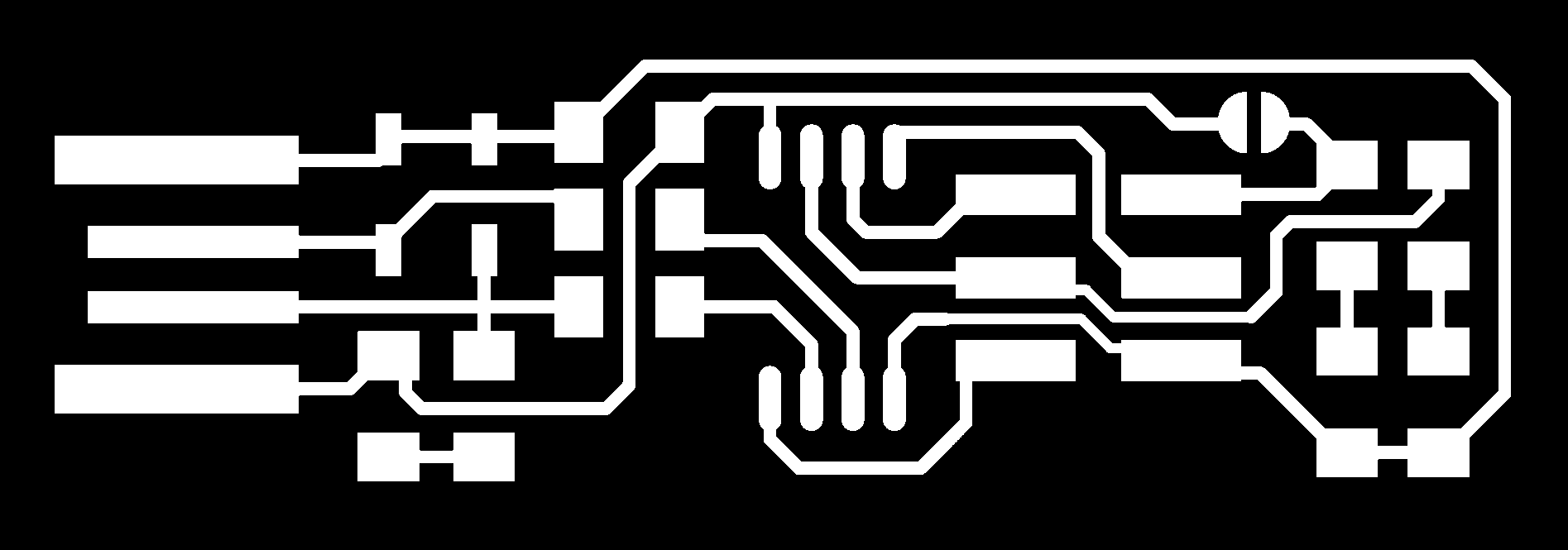
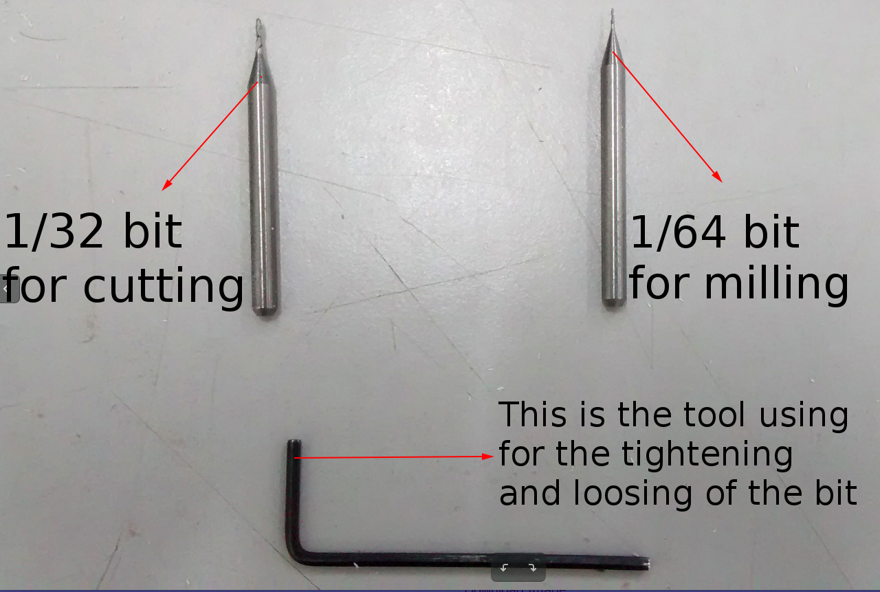
The image is black and white png formate.Here the white portion milled out through the 1/64 inch bit.
DOWNLOAD THE PNG FILE FOR OUT LINE CUT OUT

Here the out line png file is cut out through 1/32 inch bit
4.THE MILLING AND THE CUTTING PROCESS
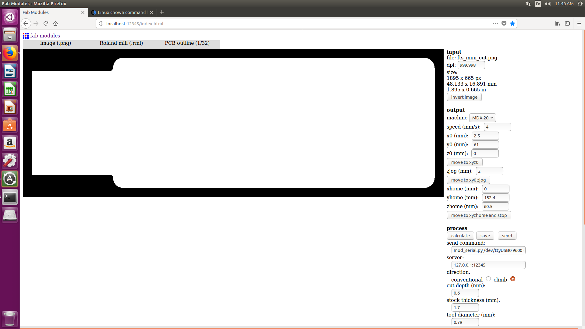
1. The fabmodule is choosen and gave the input as "image(png)file".
2.The out put as "Rolandbmill (.rml)"
3.The process of PCB trace are "1/64"
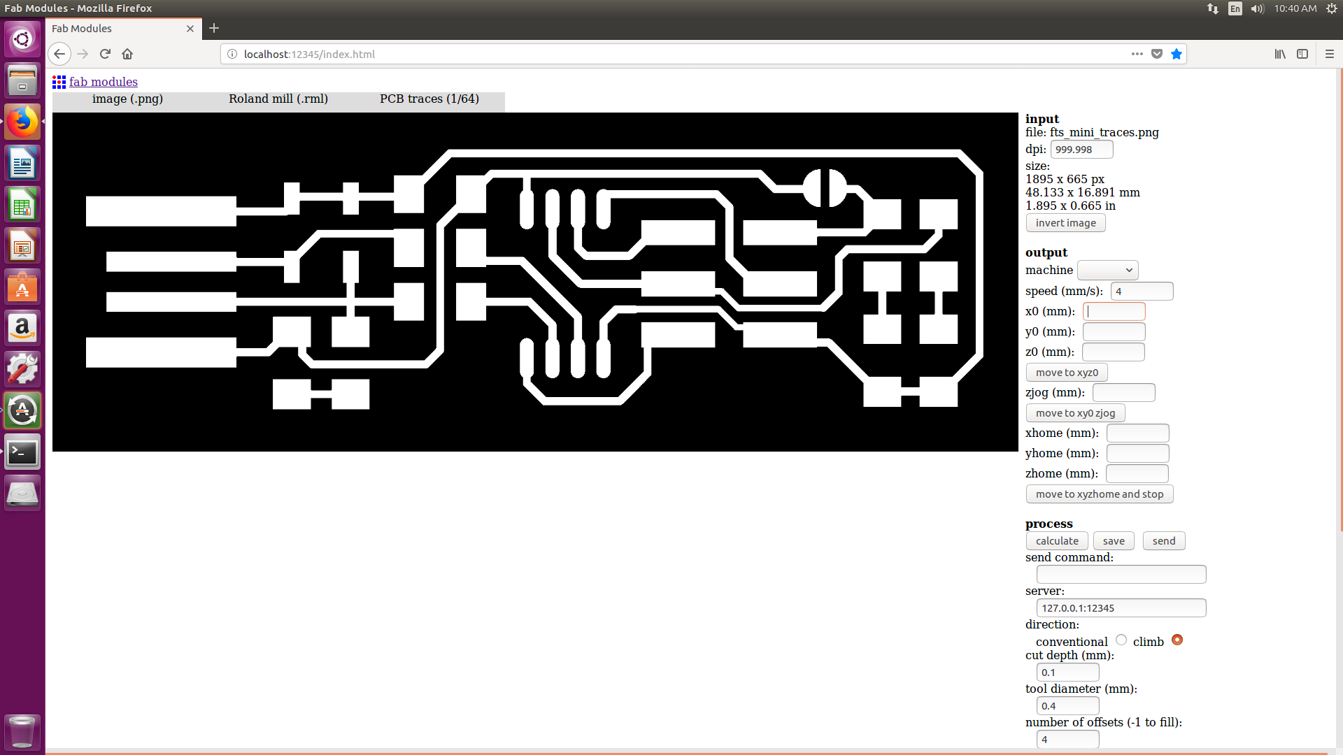
4.Then the machine is choosen as "MDX-20"
5.The origins are at the ratio of "x=2.5,y=61(for the exact position to begin)& z=0 in millimeters"

5."Cut deapth = 0.1mm & tool diameter =0.4mm"
6.Then give "calculate"(it will shows the offsets and path )
7.Then "send"
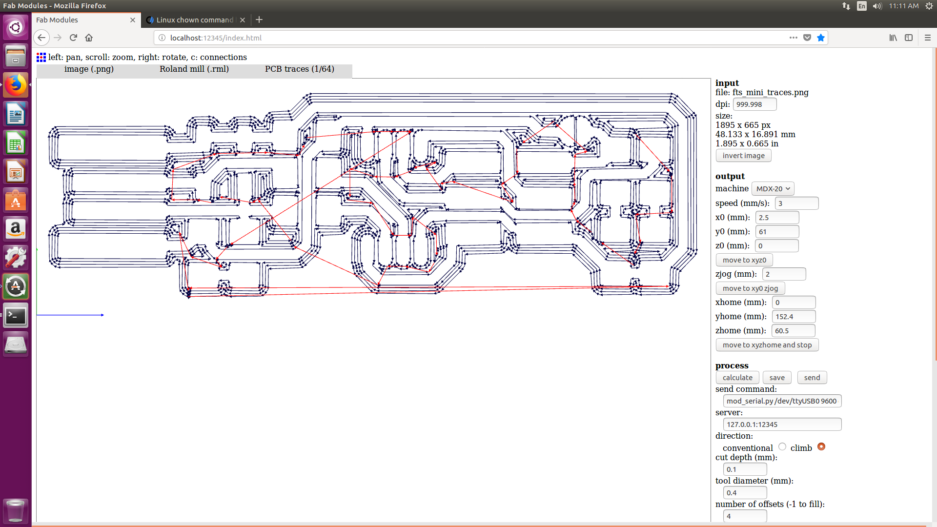
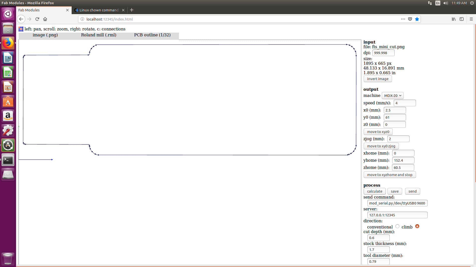
After cutting the trace then we want to cut the out line then i opend the image on fabmodule as .png .Gave the input & out put as the same but change the PCB outline as "1/32" for the cutting of the board
After giving the exact "xyz" origins gave the cut deapth =.6mm & tool diameter =.79mm .Then calculate < send.
ERROR OCCURED
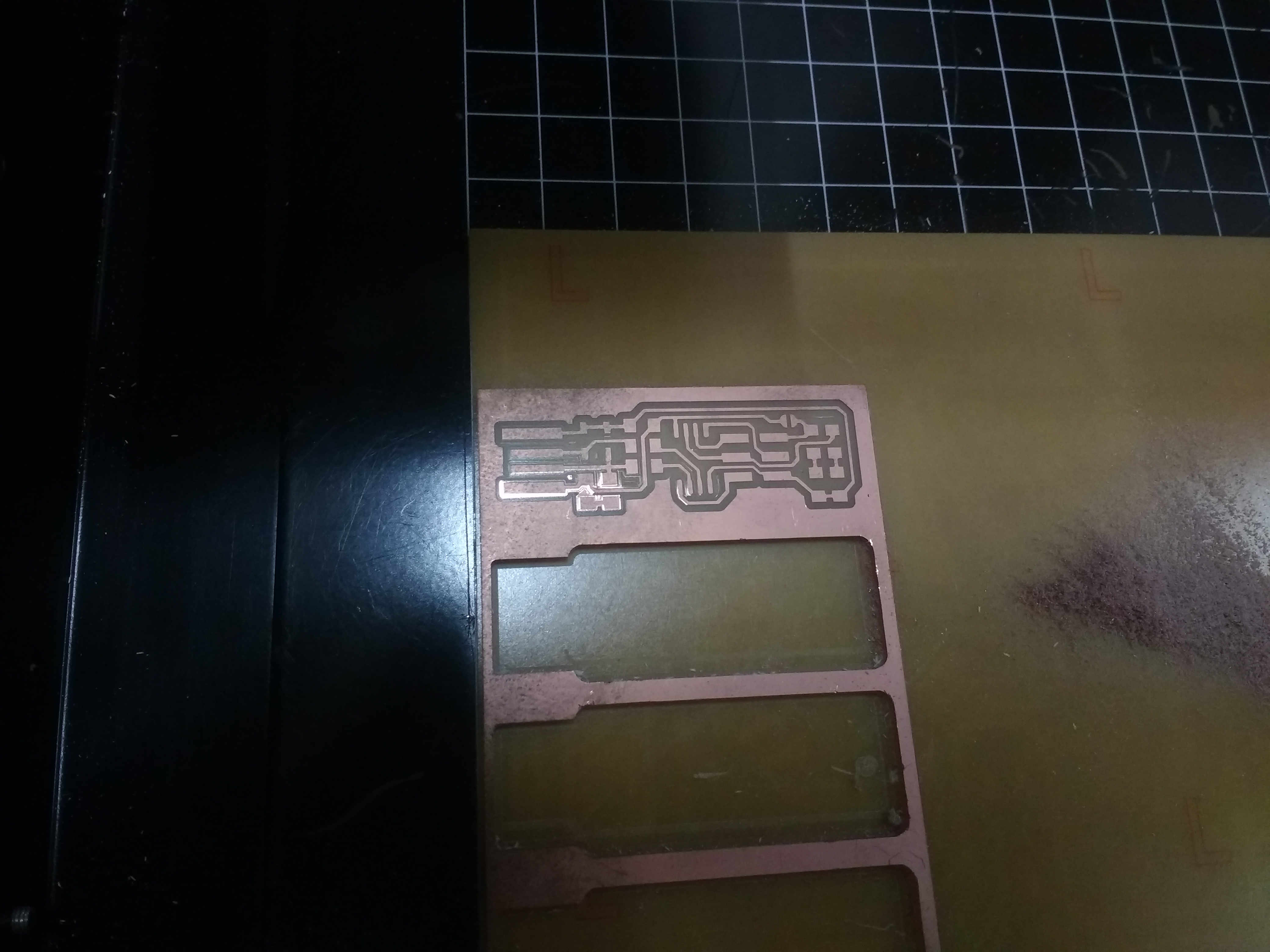
When I milled the PCB some parts willnot milled clearly .It something due to the bent in PCB bord the bit couldnot milled out copper perfectly
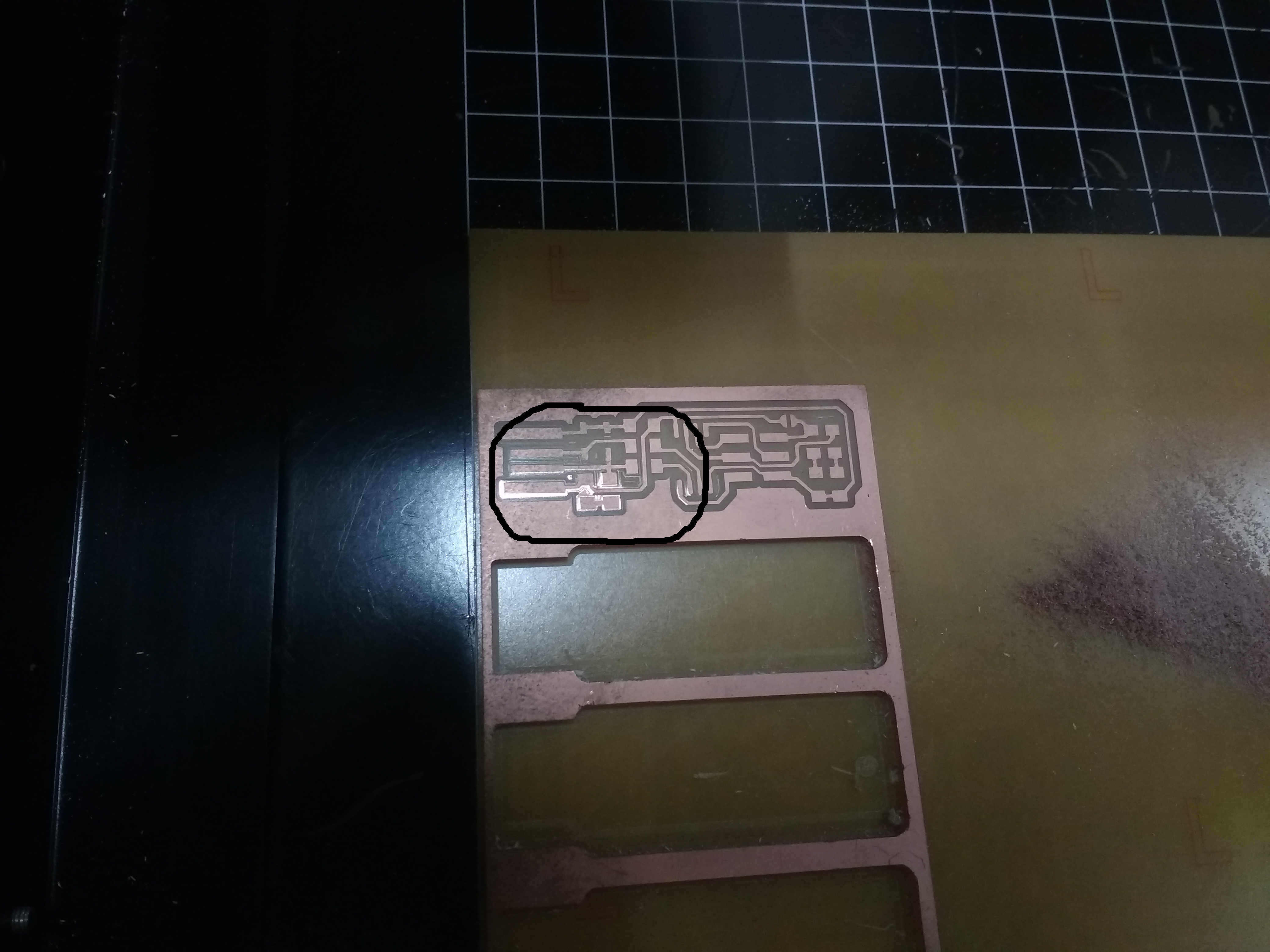
Then I cleared it with knife edge ,and make the path better for fixing electrical components and soldering
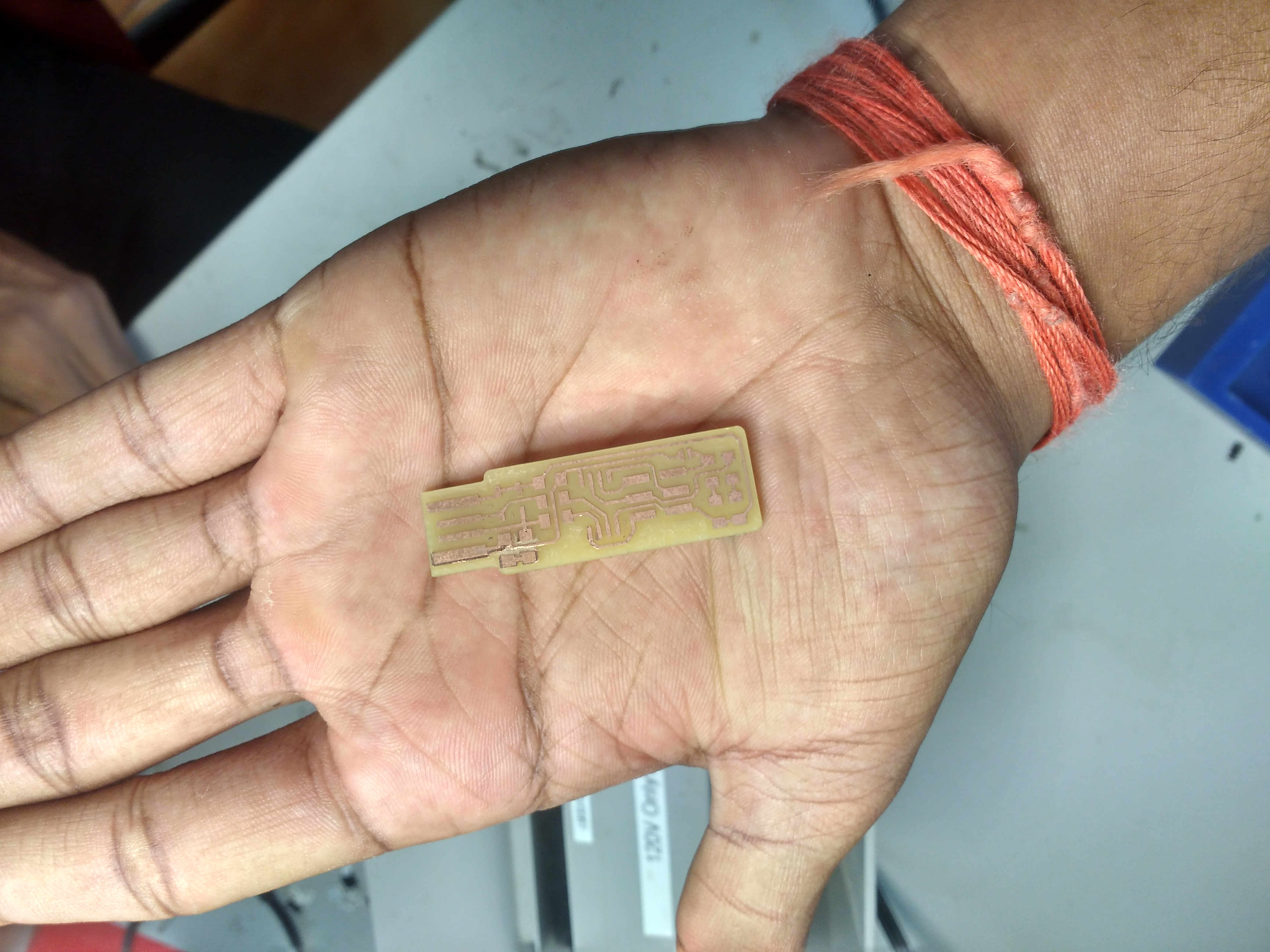
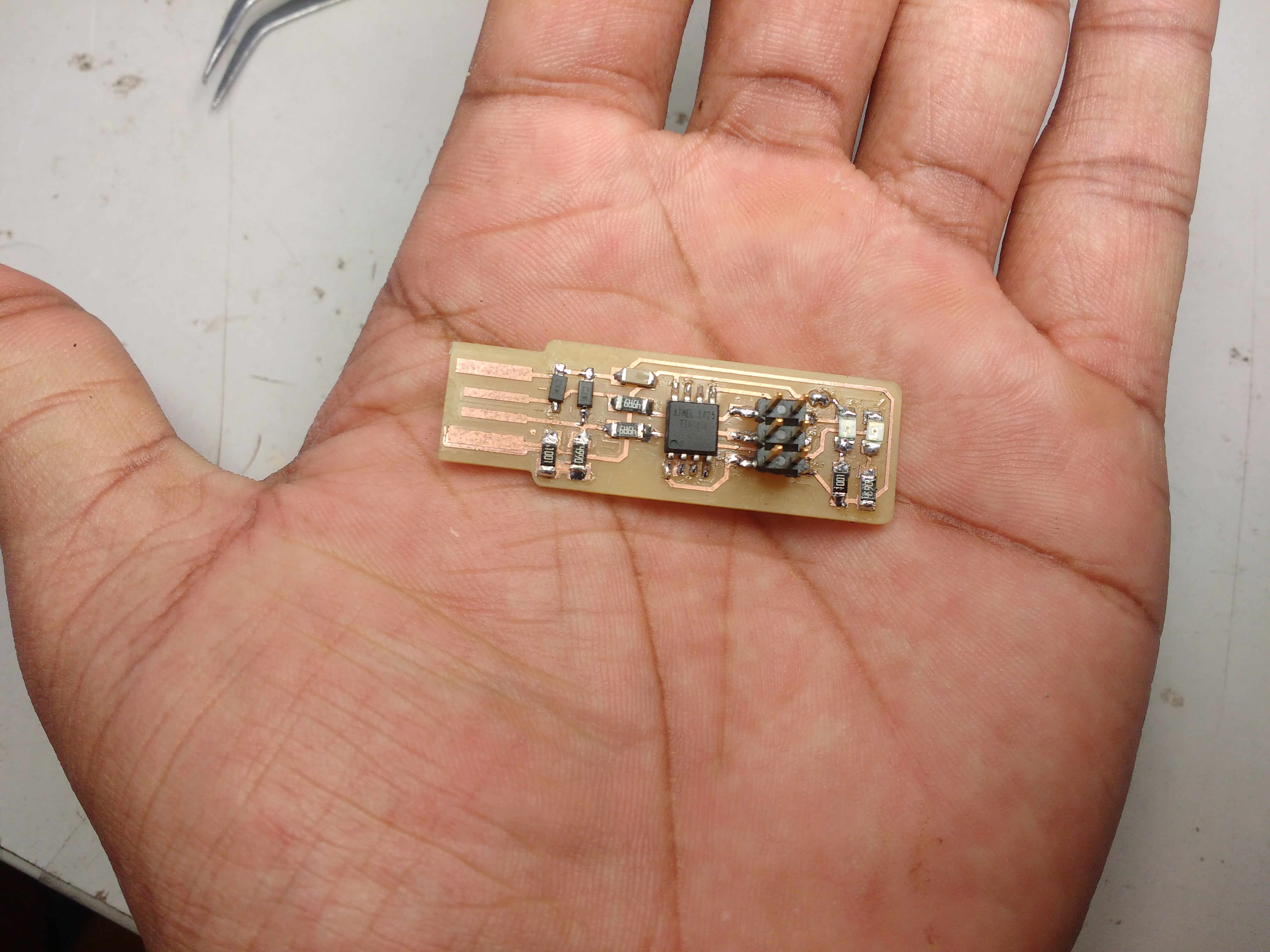
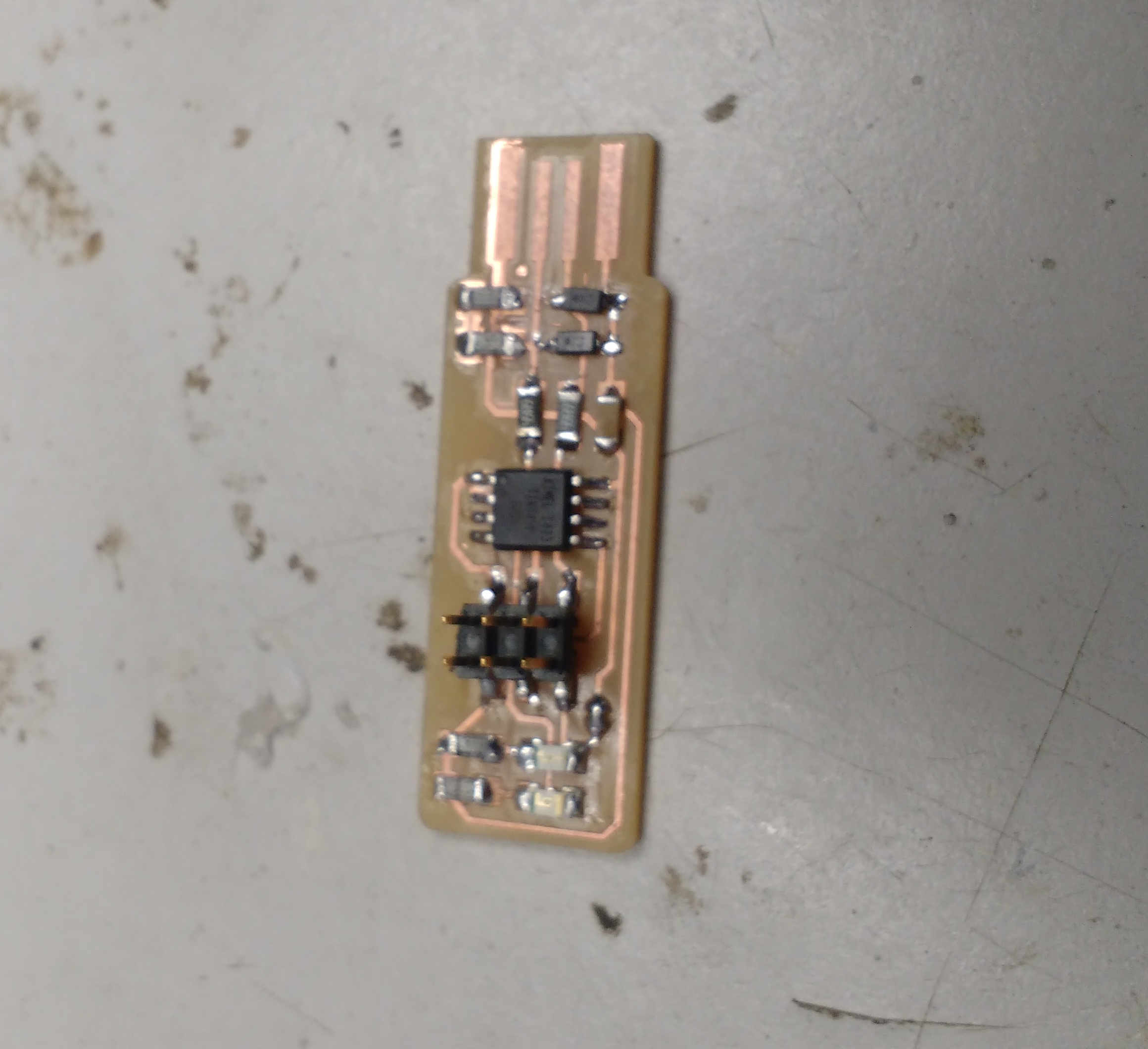
SOLDERING
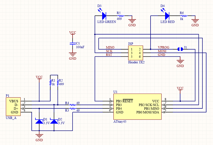
Here was the complete arrangement of electrical components on our cut out PCB through soldering . Brian explained the complete array of components in his page it helped as for easy soldering of the component very well
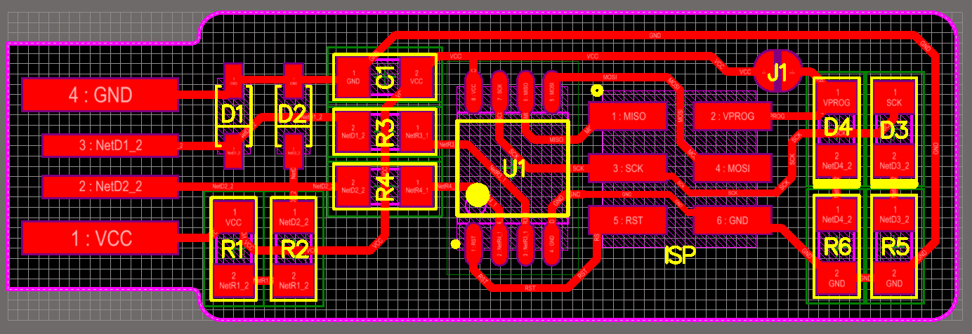
He also explained the arrangement through a schematic diagram it helps us in correct orientation of the components
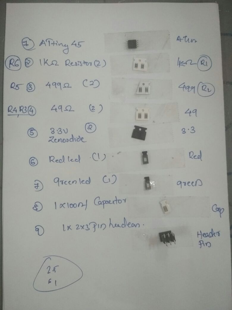
The required component were listed on a paper and pasted the components onthe paper for easy picking when soldering process
Soldering is very difficult process and it take more time for make a perfect soldering .It works on our skill the solder and the led at exact position can make shiny solder face with our components ,I tried my best for making the soldering shiny
ERROR OCCURED
When the soldering process it will take more time for making a clean face somany times the lead went over folwed on the board then I managed it with resoldering pump .
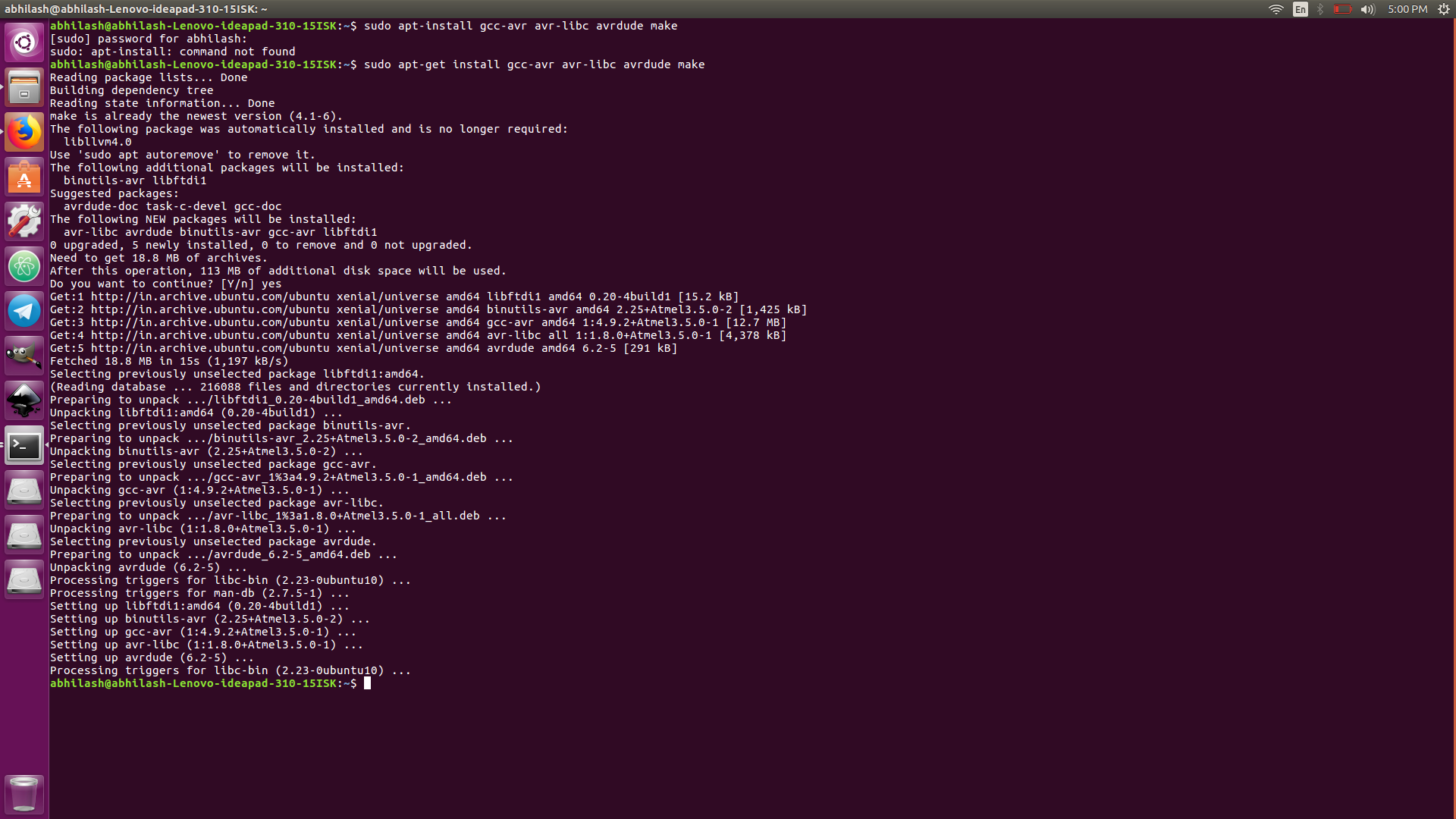
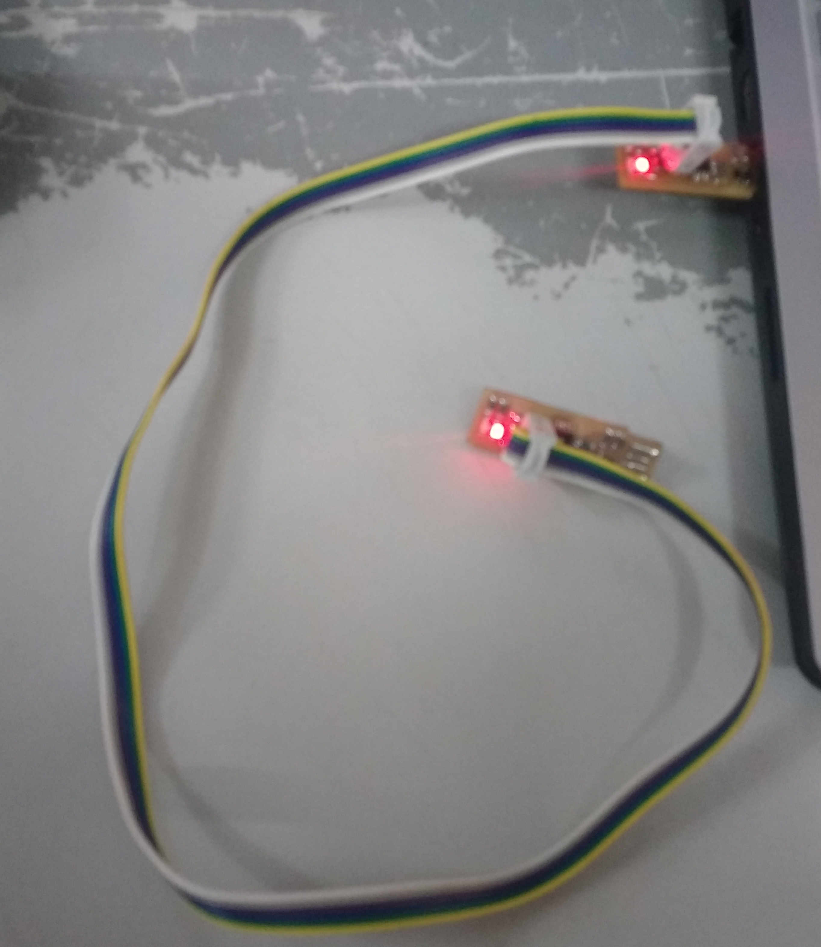
5.PROGRAMMING
For the programming I connected by a wire with a already programmed device and with the pc .Then installed the programme for working through terminal
sudo apt install avrdude gcc-avr avr-libc make
Then download the FIRMWIRE SOURCE CODE and extracted it.
When the source code is download it is in .zip file and then extracted it .After the extraction the file is in the soft state we want to make it onto "firmwire.hex" ,type the command Run make to the terminal.Then the file converted to the .hex file
then opend "makefile" for changing the programmer name intoUsbtiny.Then open the terminal for making flash with below commands ,we can directly connect the device with the lap.
make flash
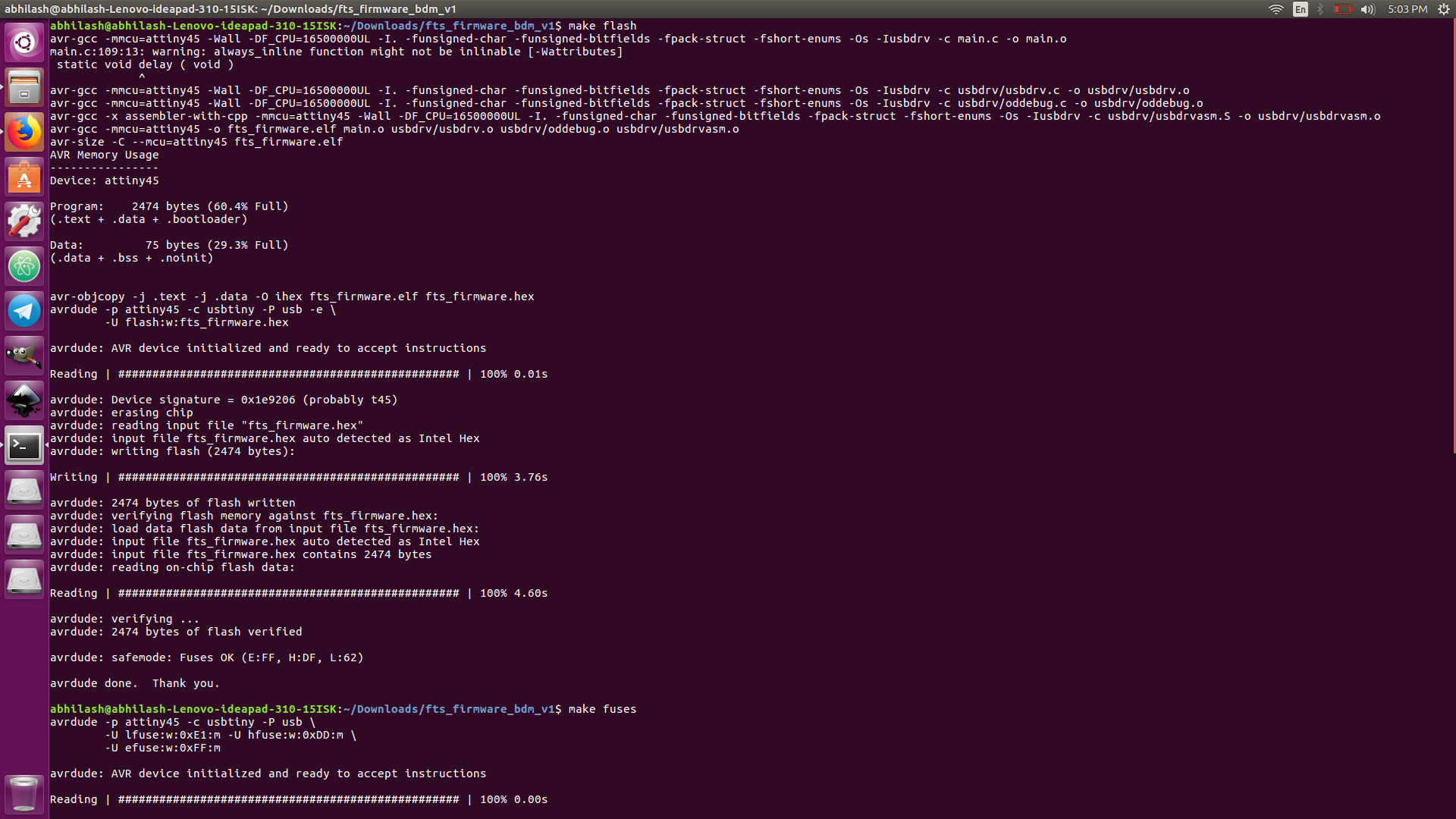
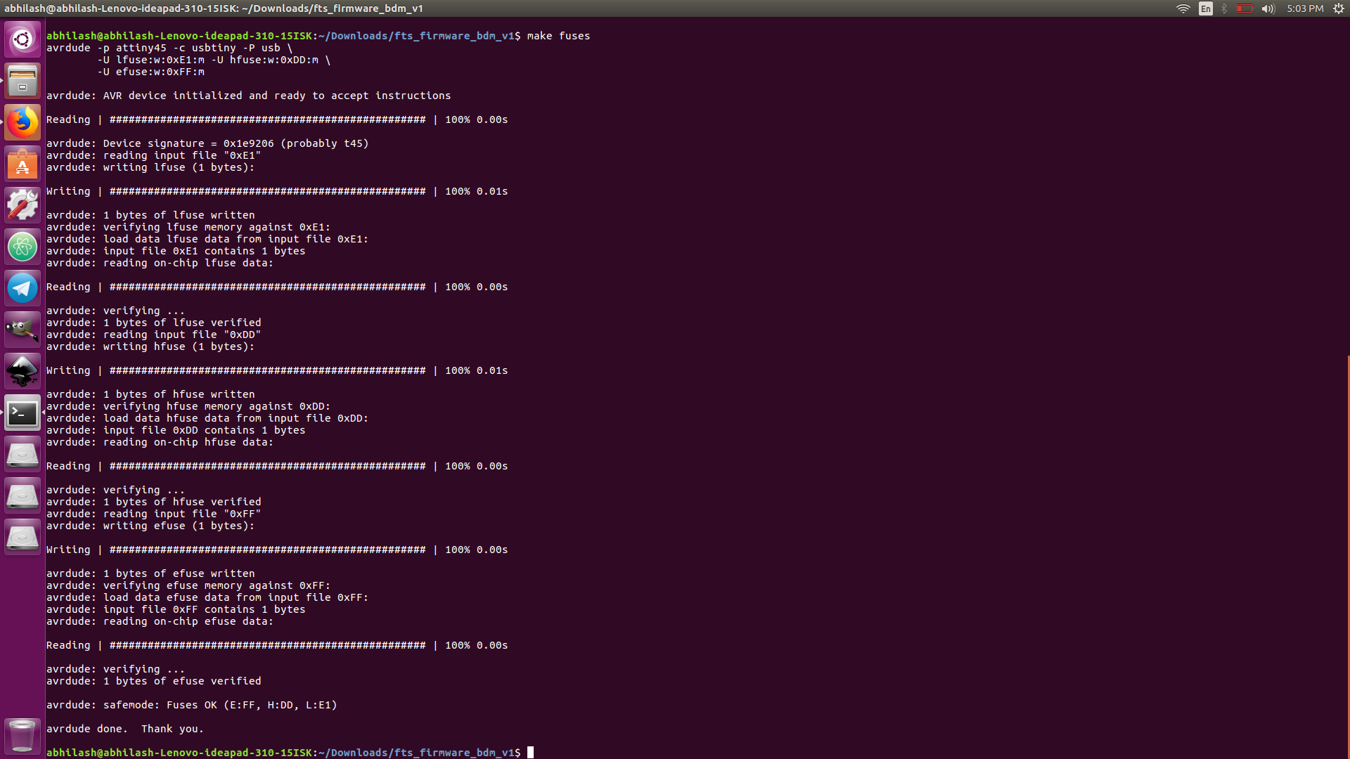
make fuses
Then lsusb for listing the programmes in that device in terminal
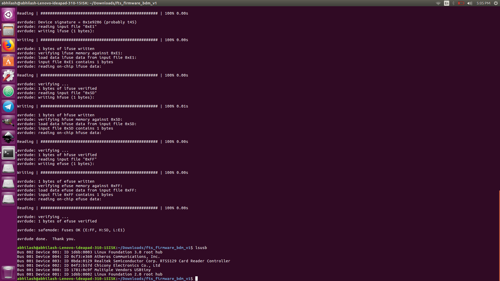
make rstdisbl : For disabling the reset pin in our programmed device ,
and now we have the programmed device we can use this device as a programmer for furthure programming of another device