Electronic design
Two week ago, I have used KiCad to design a double sided PCB. I ll design this week circuit assignment using Auto-desk Eagle software.
Eagle
Eagle could be easily dowloaded on linux from Auto-desk page link. As most electronic design software, Eagle follows the same procedures, you sketch your schematic diagram then you route the wire using PCB design.
Schematic
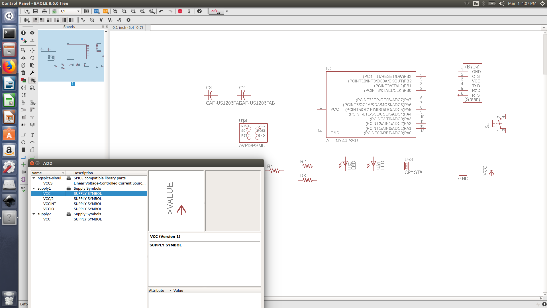
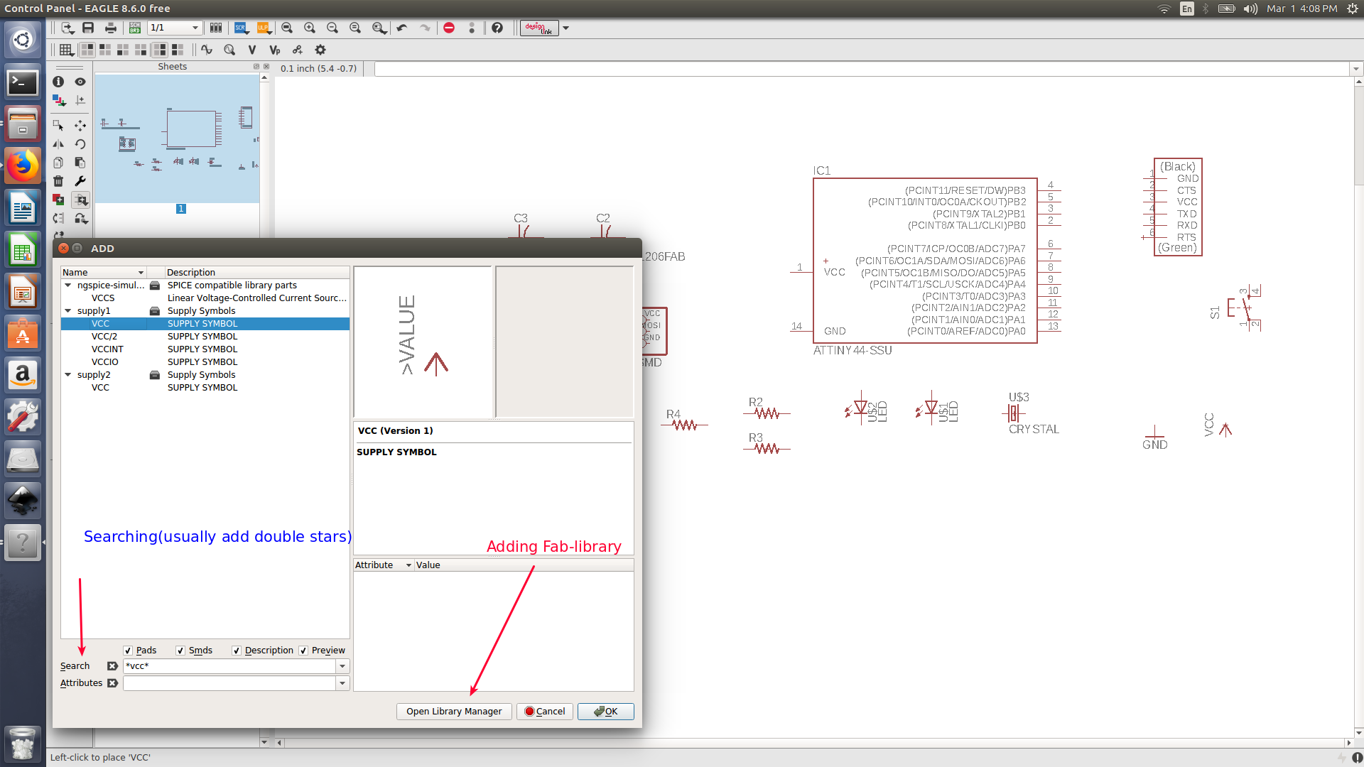
- Some of the electronic devices were unavailable at the add tab, I had to add Fab library (available at 5th week class schedule). To do that just save it as a link and open the
library managerafter accessing theadd tabthen simply browse for fab library ad add it. Labelis an easy way to connect between wire, without actually dragging a real wire which would make you schematic design tidy. To do that just label the 2 devices that you want to connect with the same name and they ll automatically be connected.- I have connected by switch to PB2 via a pull down resistor.
- LED is connected to PA7
PCB design
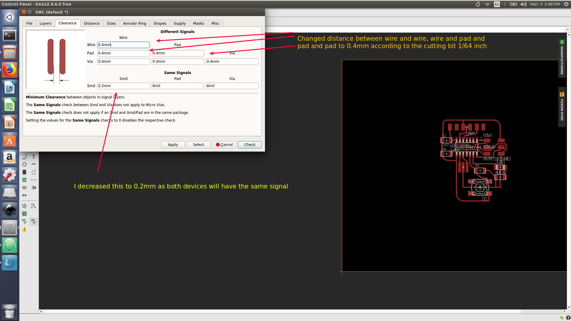
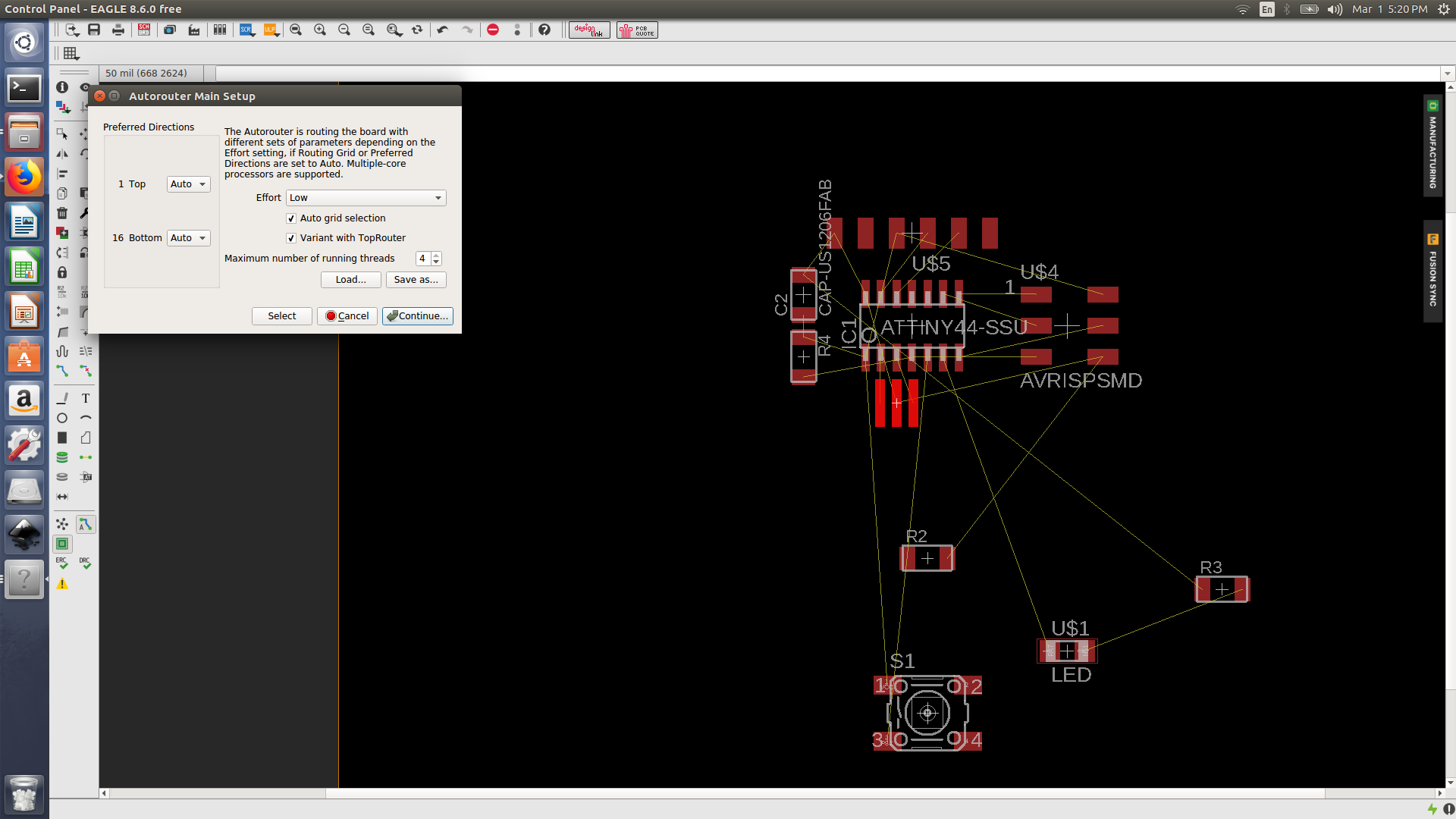
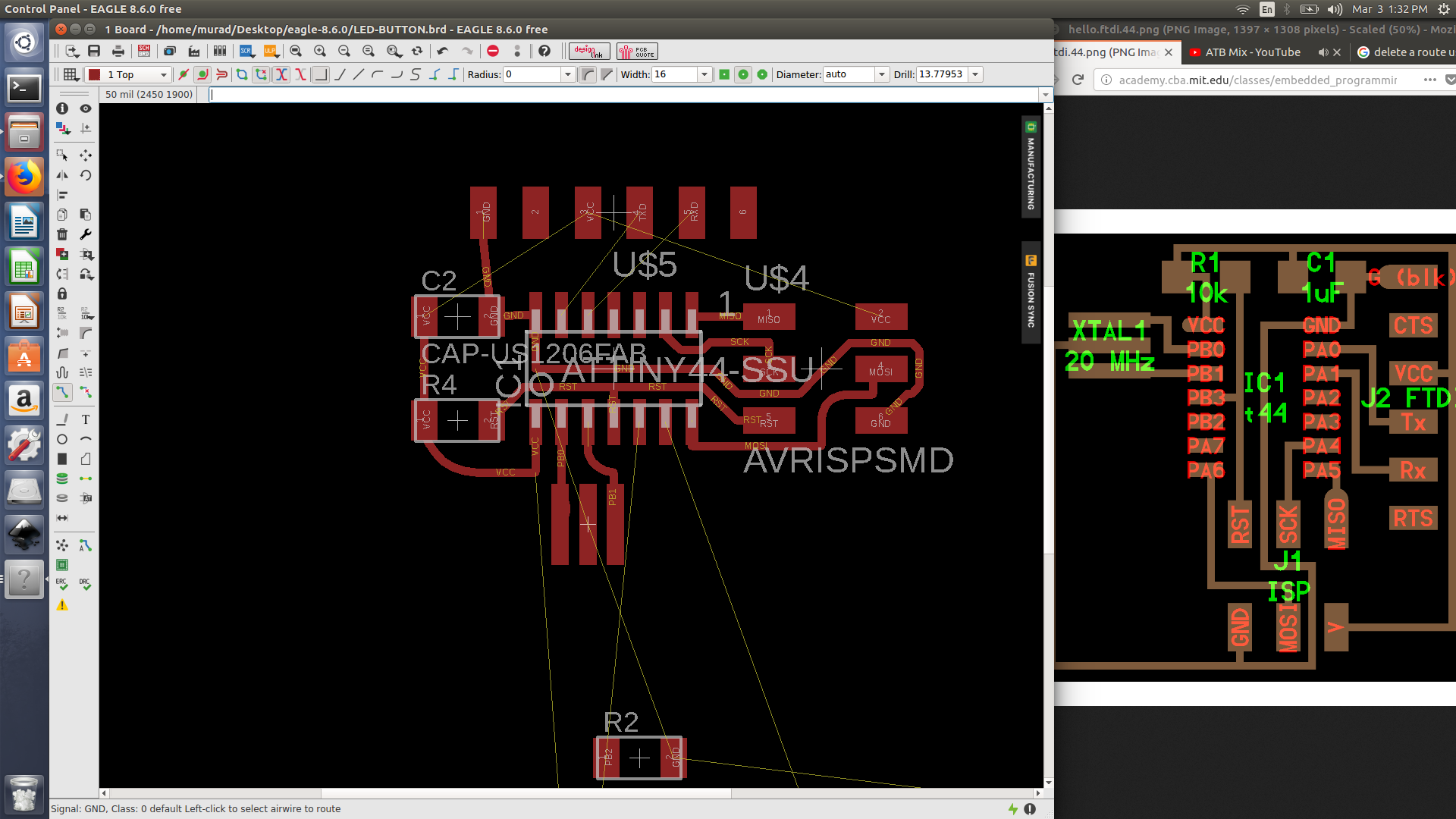
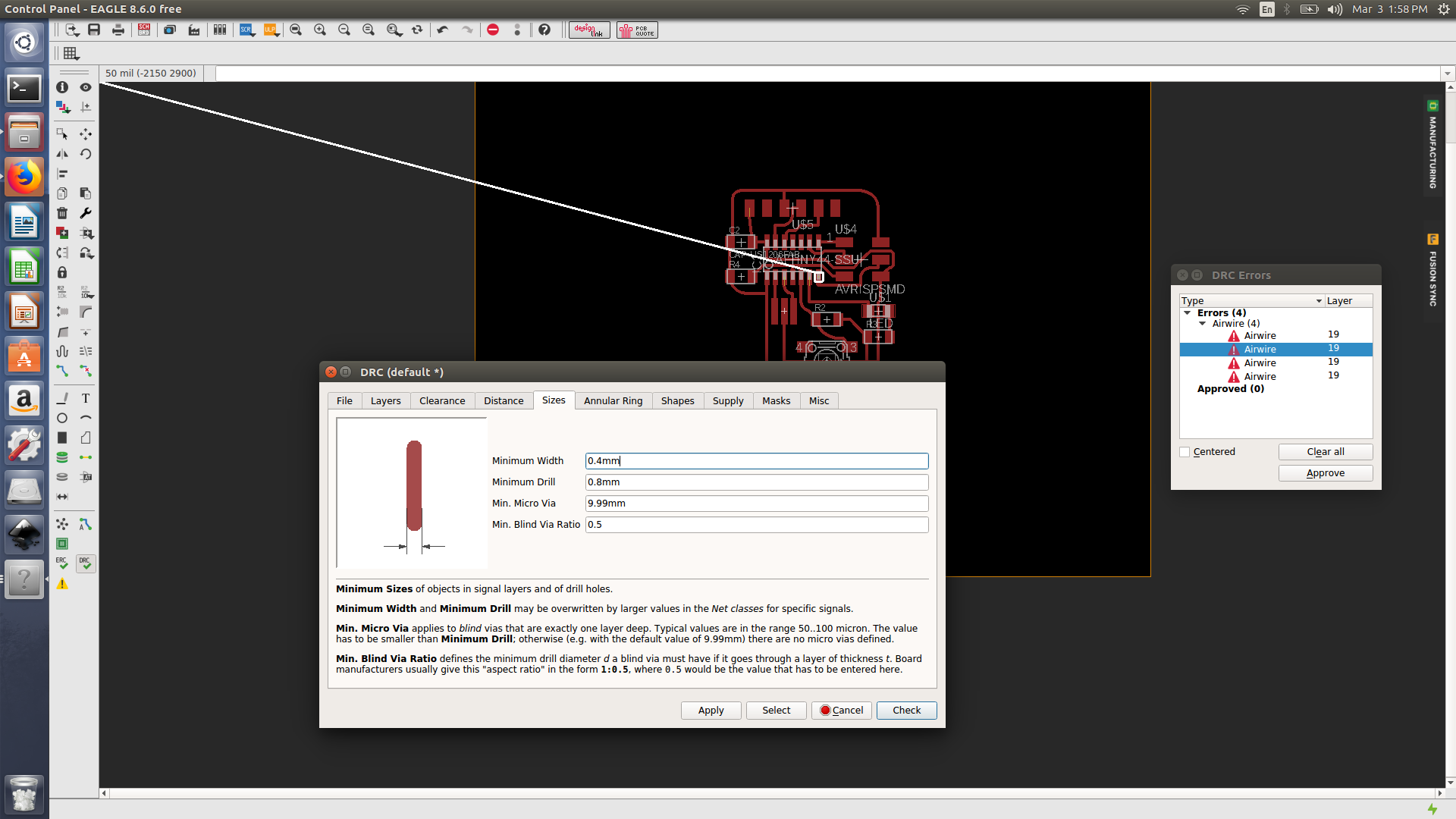
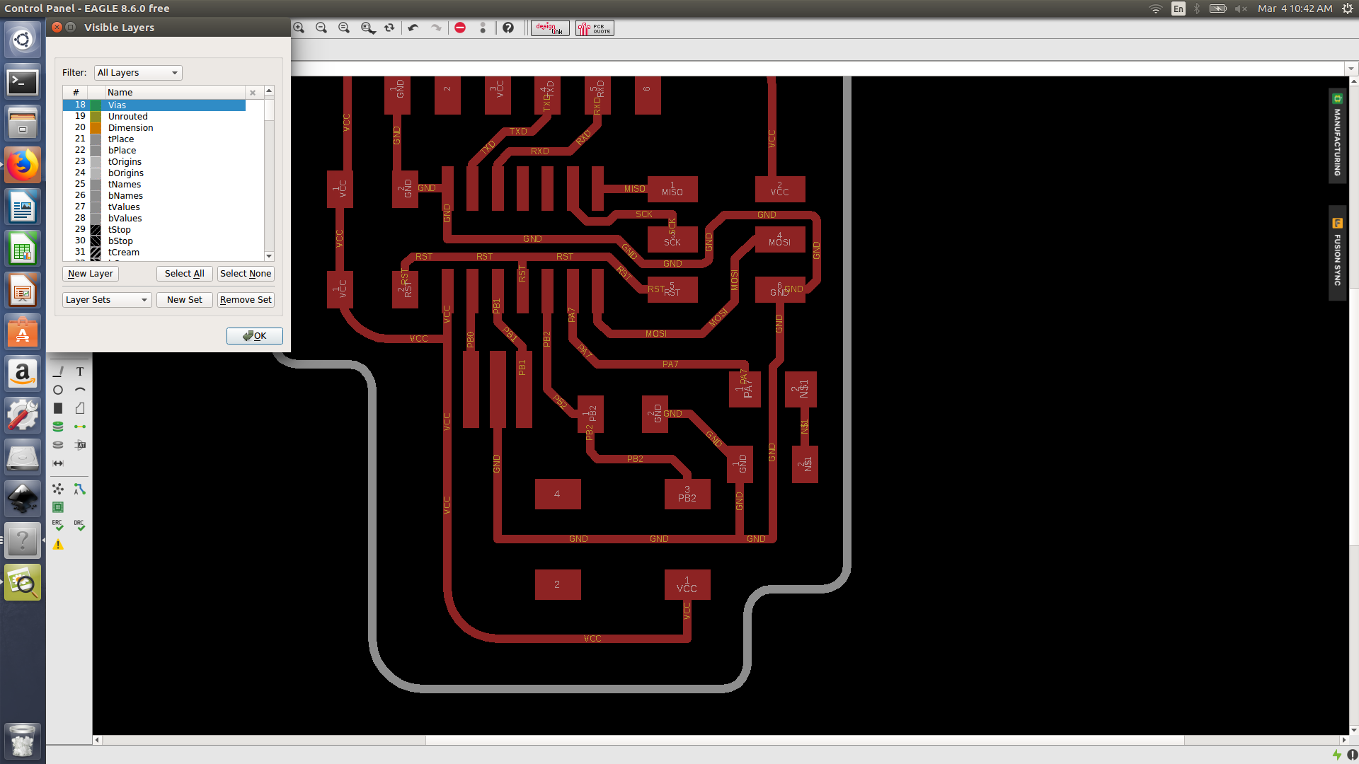
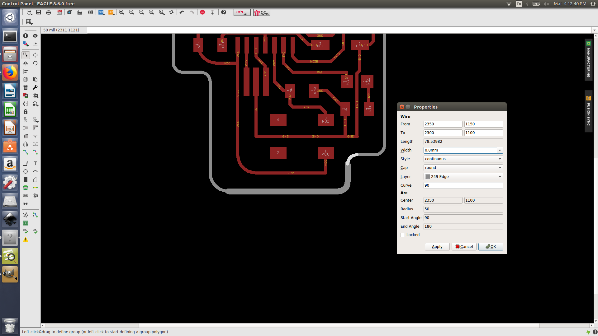
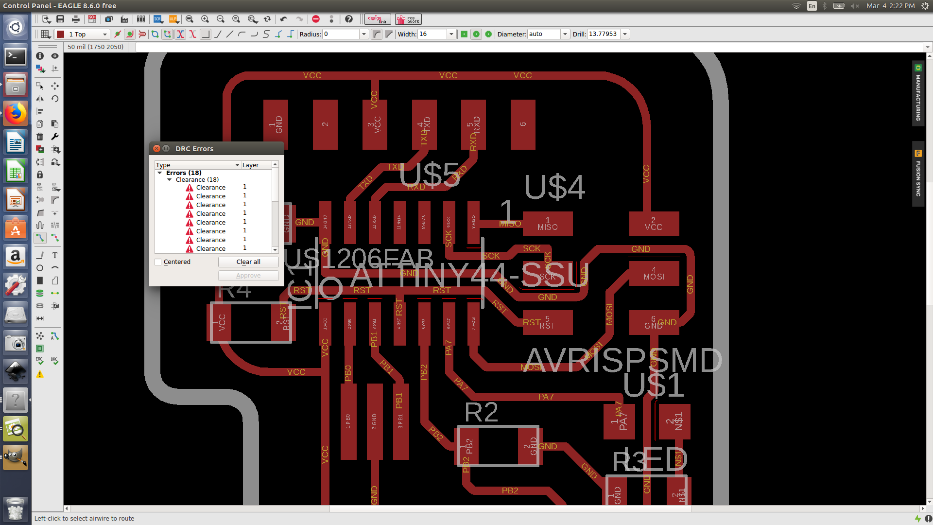
- Auto route is a feature that automatically route all your connections that you provided on the schematic sketch. To use auto route, you must first define all the design rules
DRCsuch as clearness between every wire and wire, wire and pad and pad and pad. those all must be amended to 0.4 mm as we are using 1/64 inch (0.39mm) bit to mill the traces. For the min drill, we must change it to 0.8mm as the cut bit we are using is 1/32 inch (0.79 mm). - Auto-route, does not change your devices location, it would just come up with more than a possible way to connect your wires. Its recommended to spend some time placing your devices in good place before activating the auto route
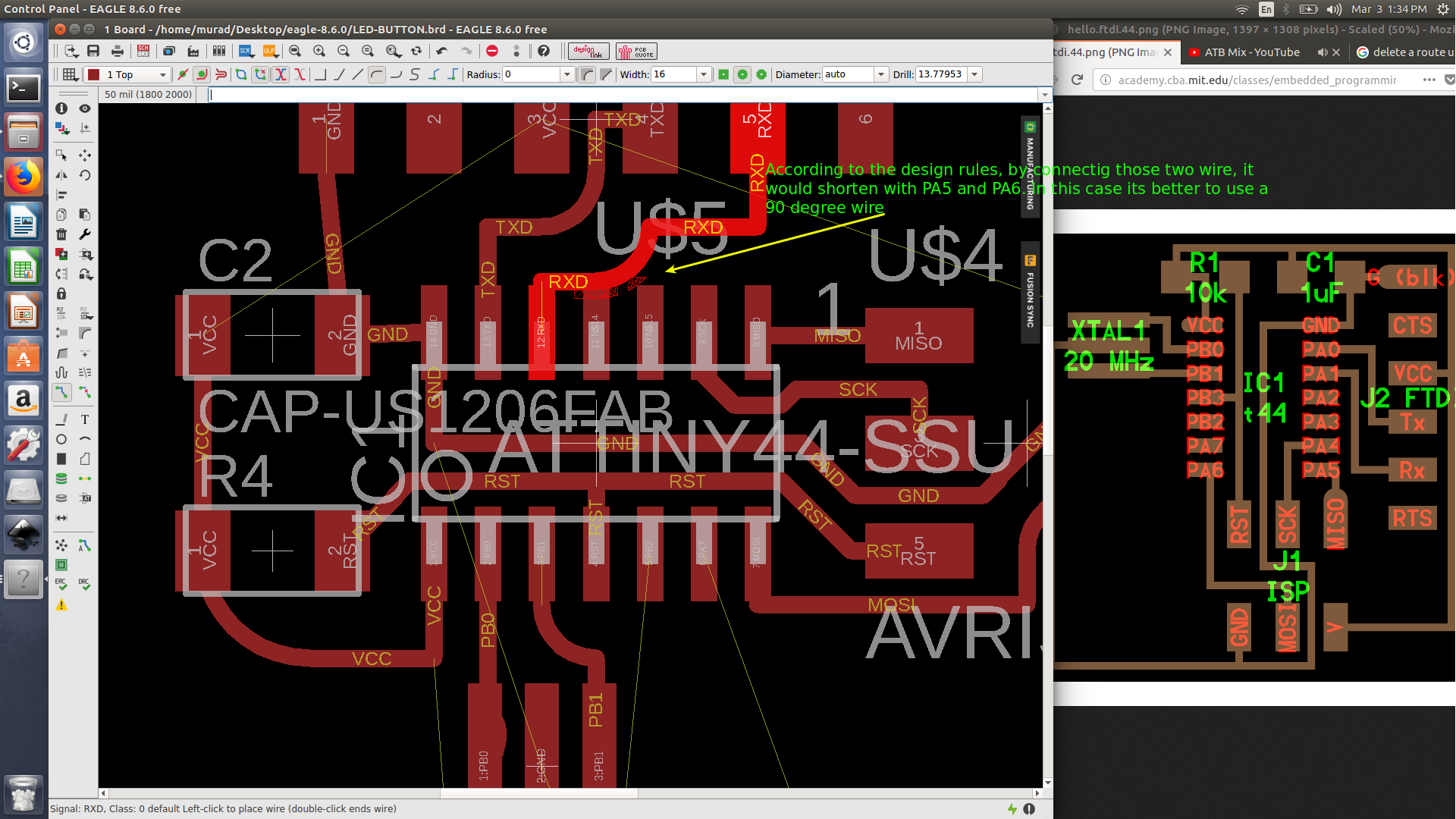
- I manually routed the connection, It’s more efficient if you have small circuit. I changed the route line width to 16 instead of 6.
- I have used wire bend 5 to create curved routes, however in some place it would take larger area compared to the normal 90 degrees wire.
Source files
download schematic filedownload Pcb design file
Problem Faced
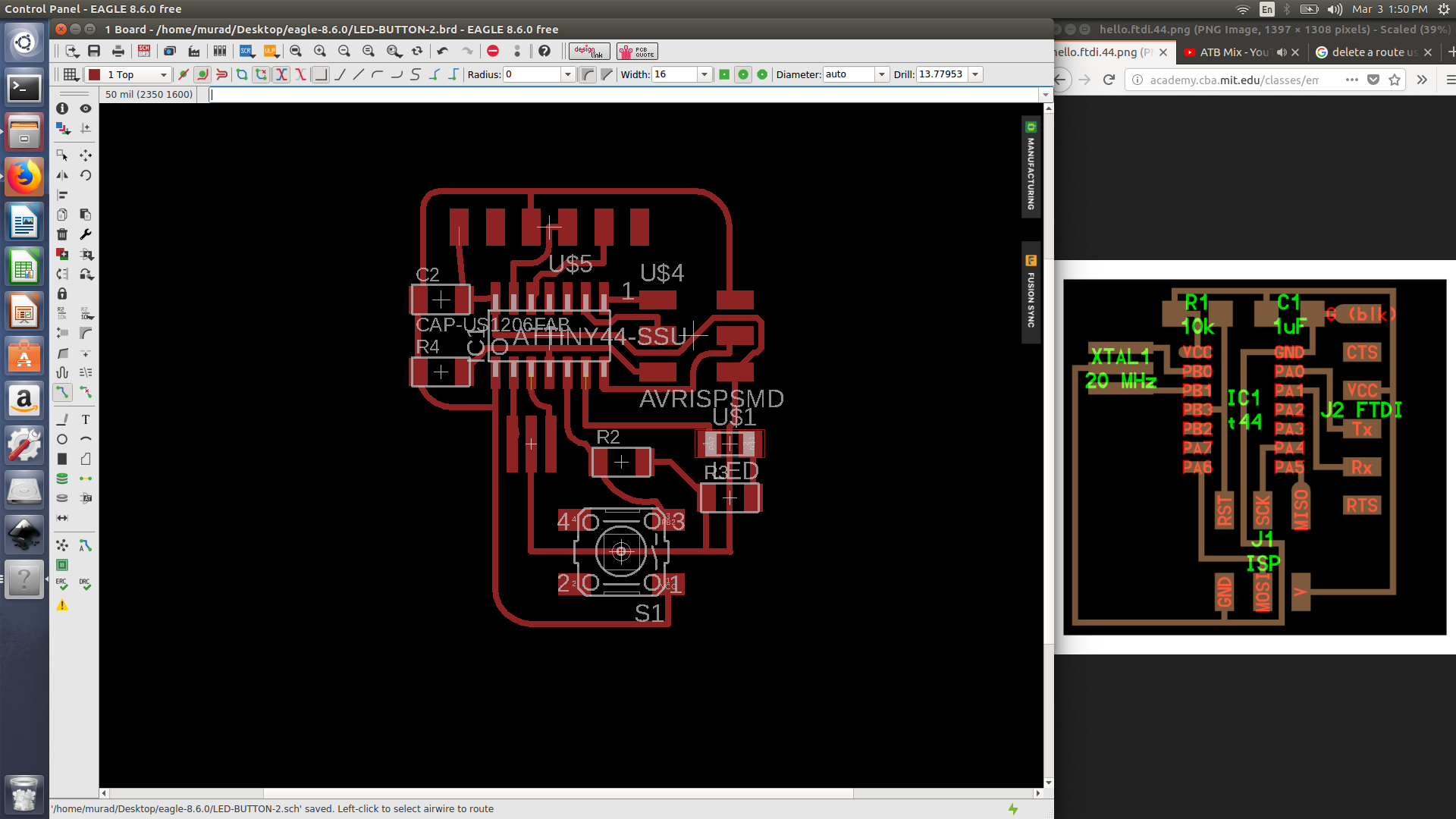
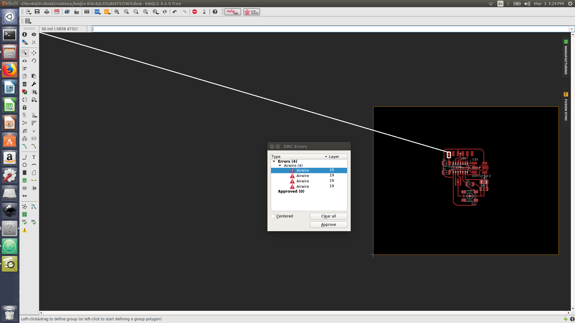
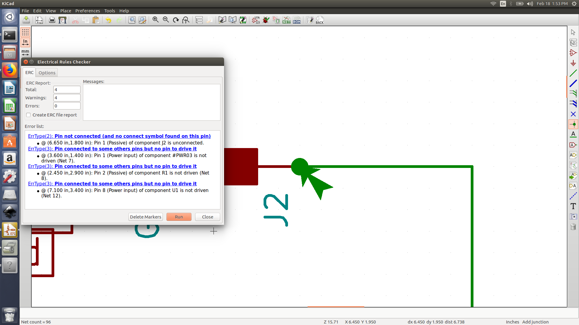
- After routing all my connection, I used
DRCto check my connections. I have got 4 error messages which shows air wires and a wire directing to outside the design area. I tried to show the global hidden air wire by usingratnestas rat-nest is a command that shows all air-wire and achieve the shortest path, but that didn’t work for me as those long wire lead no where.
Exporting pcb design
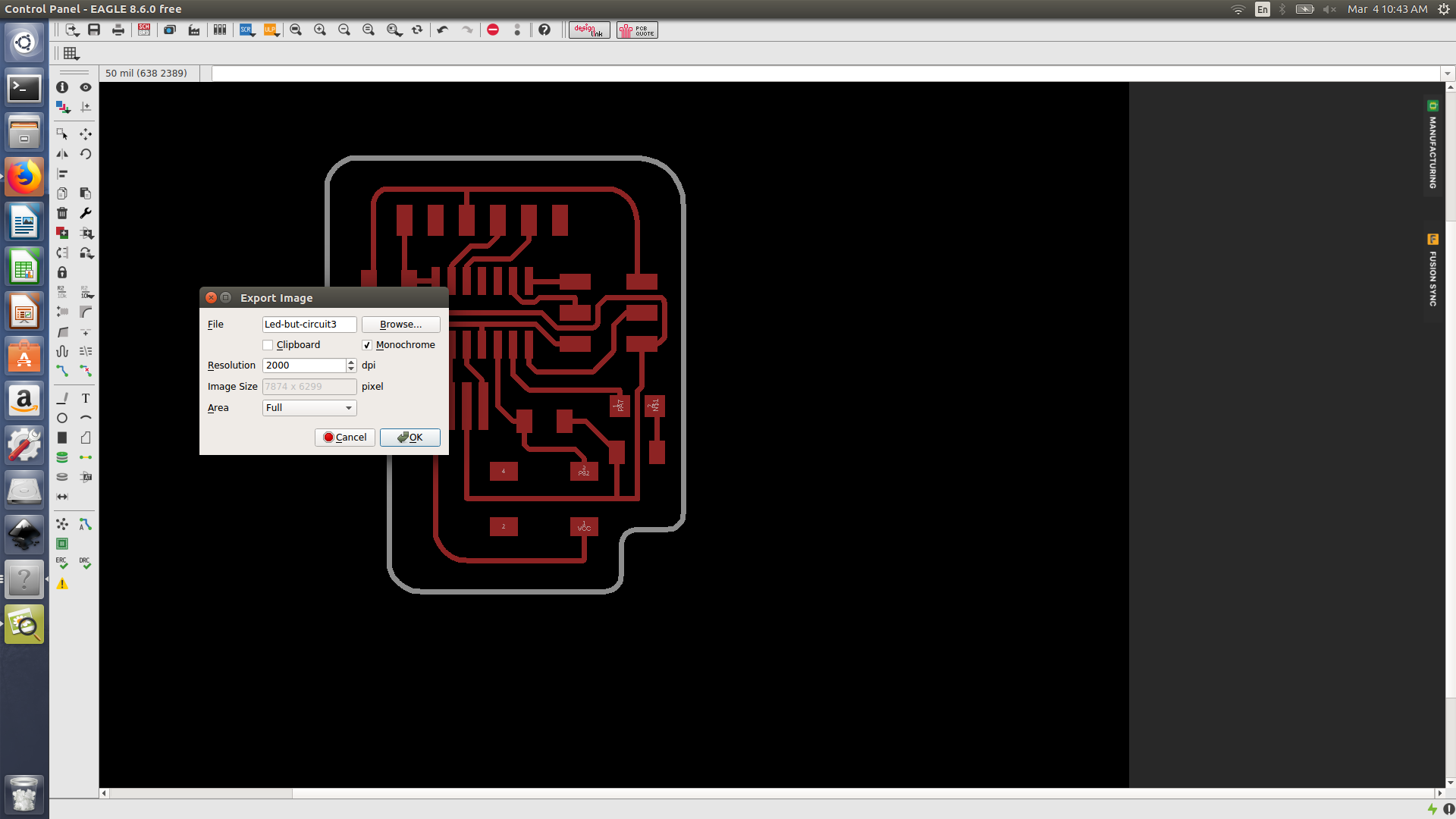
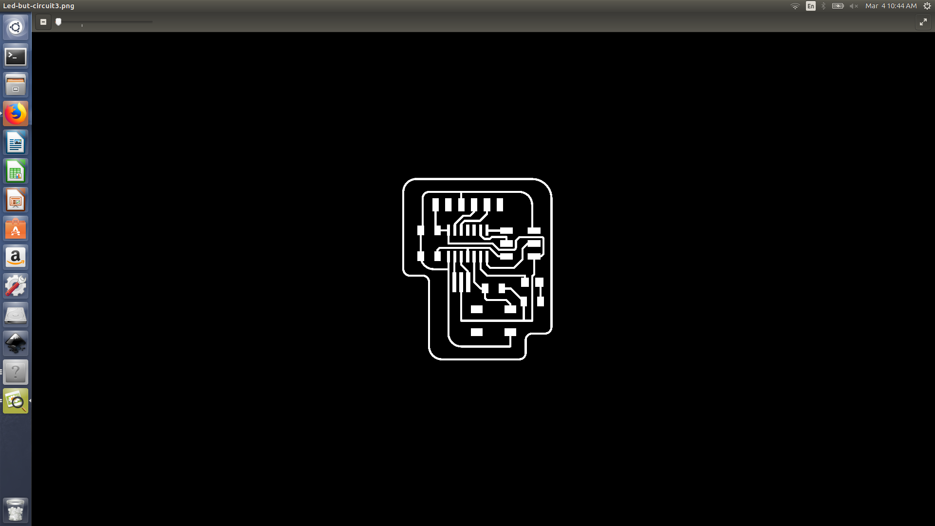
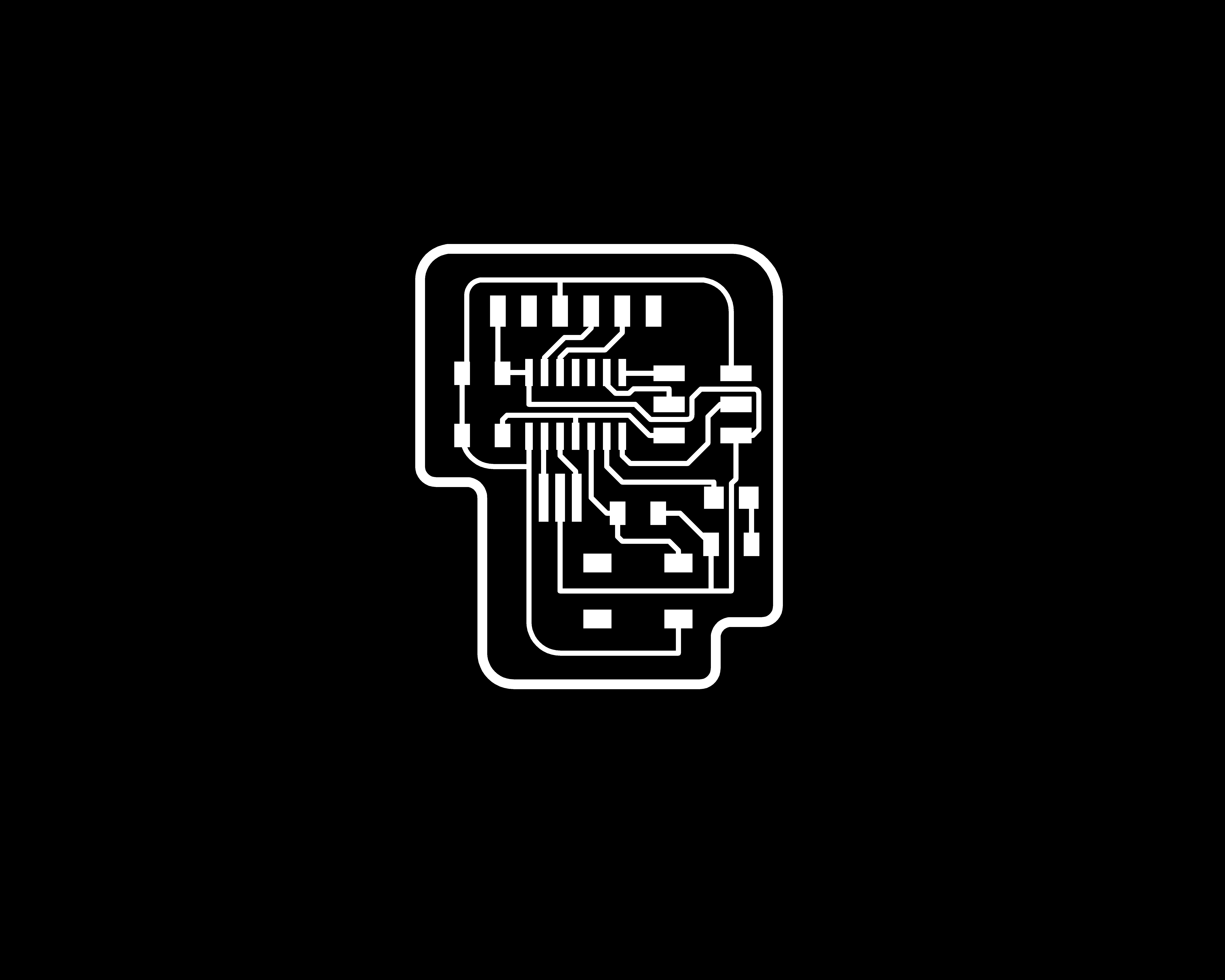
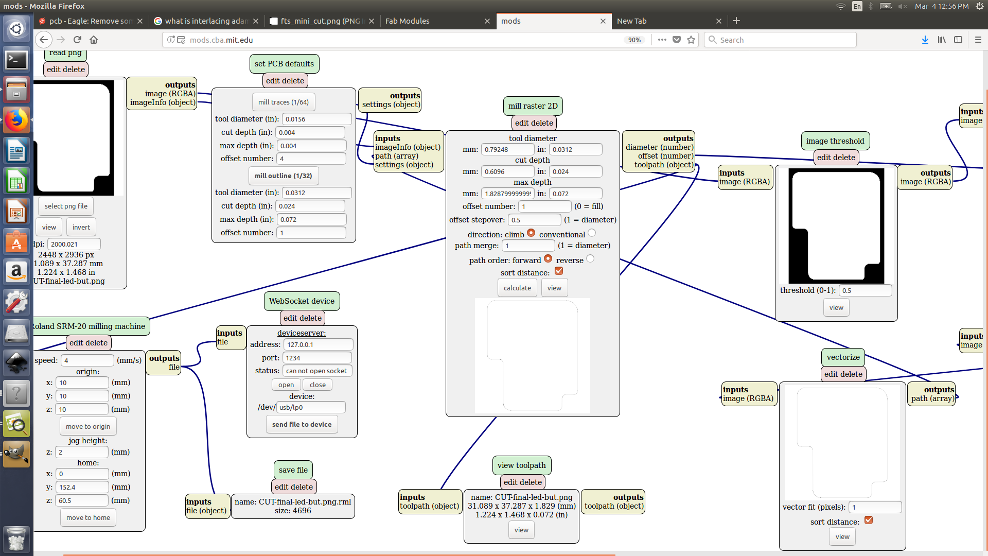
- I exported the circuit as a png image as this format is acceptable by SRM-20 to
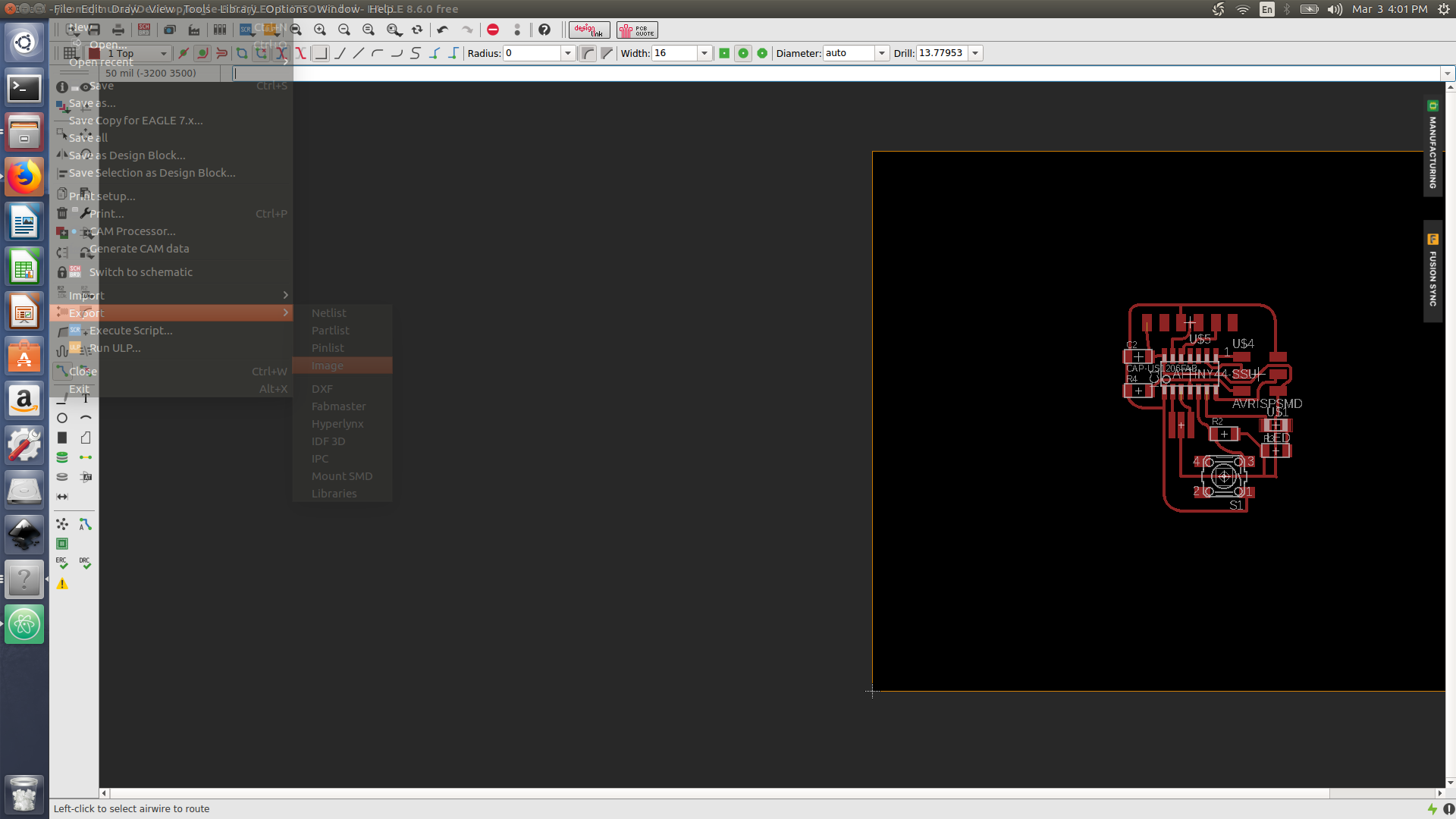
- I set the export parameters to 2000 pixels and mono-chrome ( black and white)
-
I have faced a problem as I have exported the image with the labels, names, value etc. I deactivated them by accessing
layer settingtick them off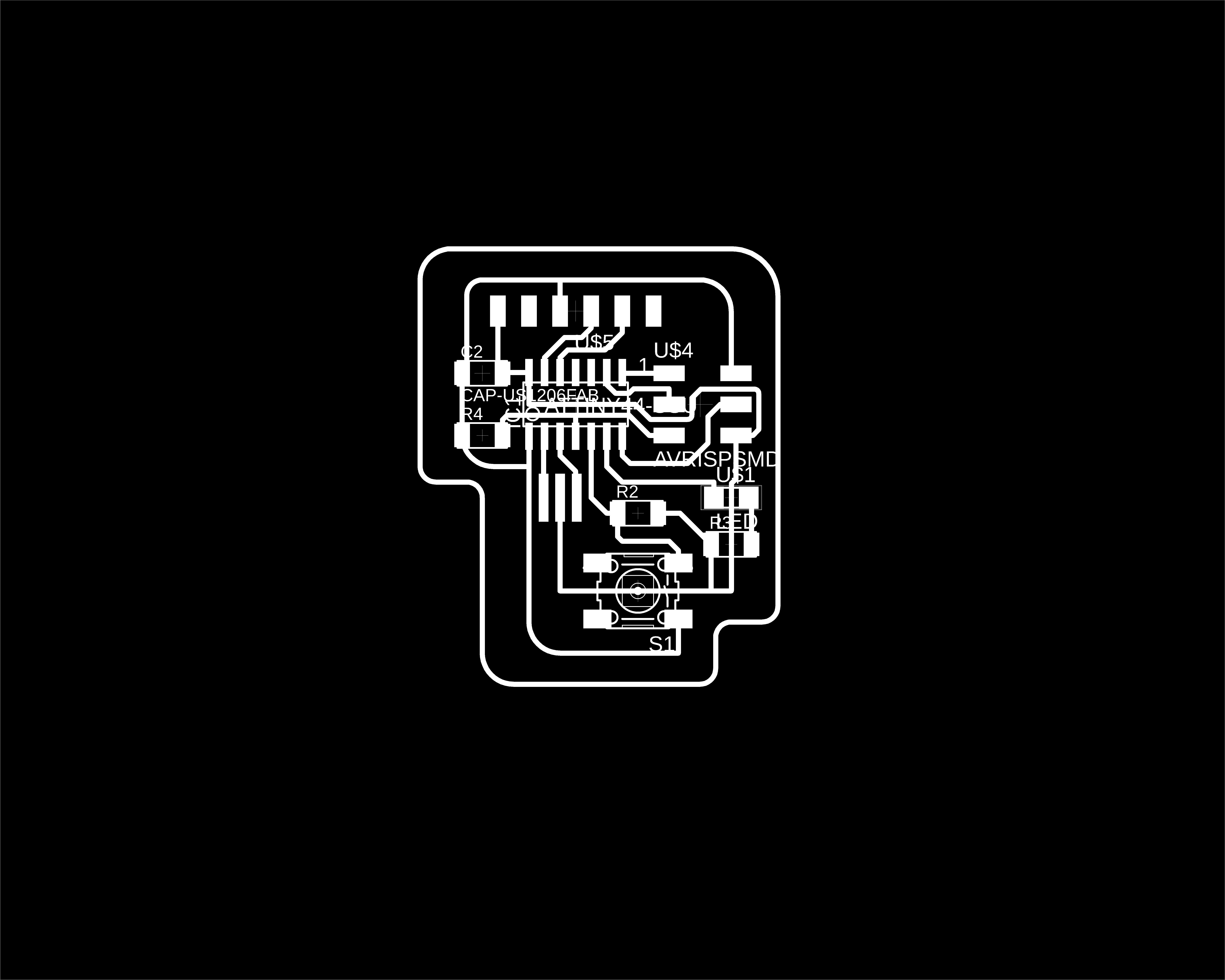
- I used Gimp to edit and crop my circuit images. I have created a traces image and a cut image.

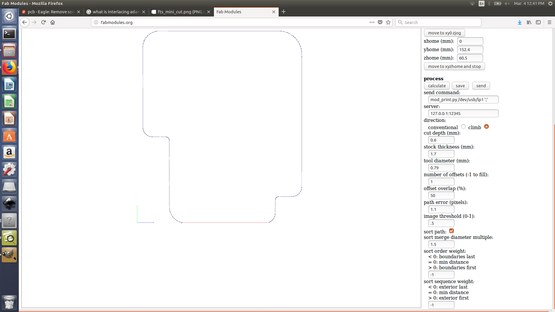
- I then created the rml file using mods, however one problem i faced is than the cutting line width was very so I have amended it in the design to 0.8 mm ( cut pit size)
Cutting the circuit
- I have tried to use both fab modules and mods to create the rml file. I am more familiar with fab modules but honestly mods is really powerful but you must take some time going through it as for the first sight it would seem very complicated.
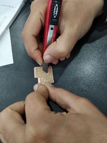
- After I cut my PCB some of the wire and pads weren’t separated properly, although I have already set my design parameter rule to 0.4 space between wire and pads. I had to manually cut the traces.
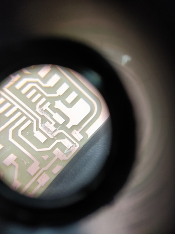
- for a better result I increased all the clearance parameter to 0.41 instead of 0.4 but this have caused several errors, I rerouted some of the wires.
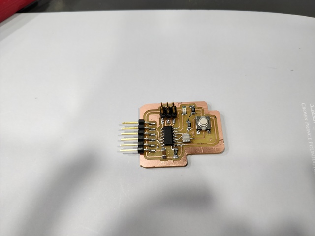
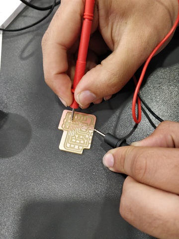
Programming the board
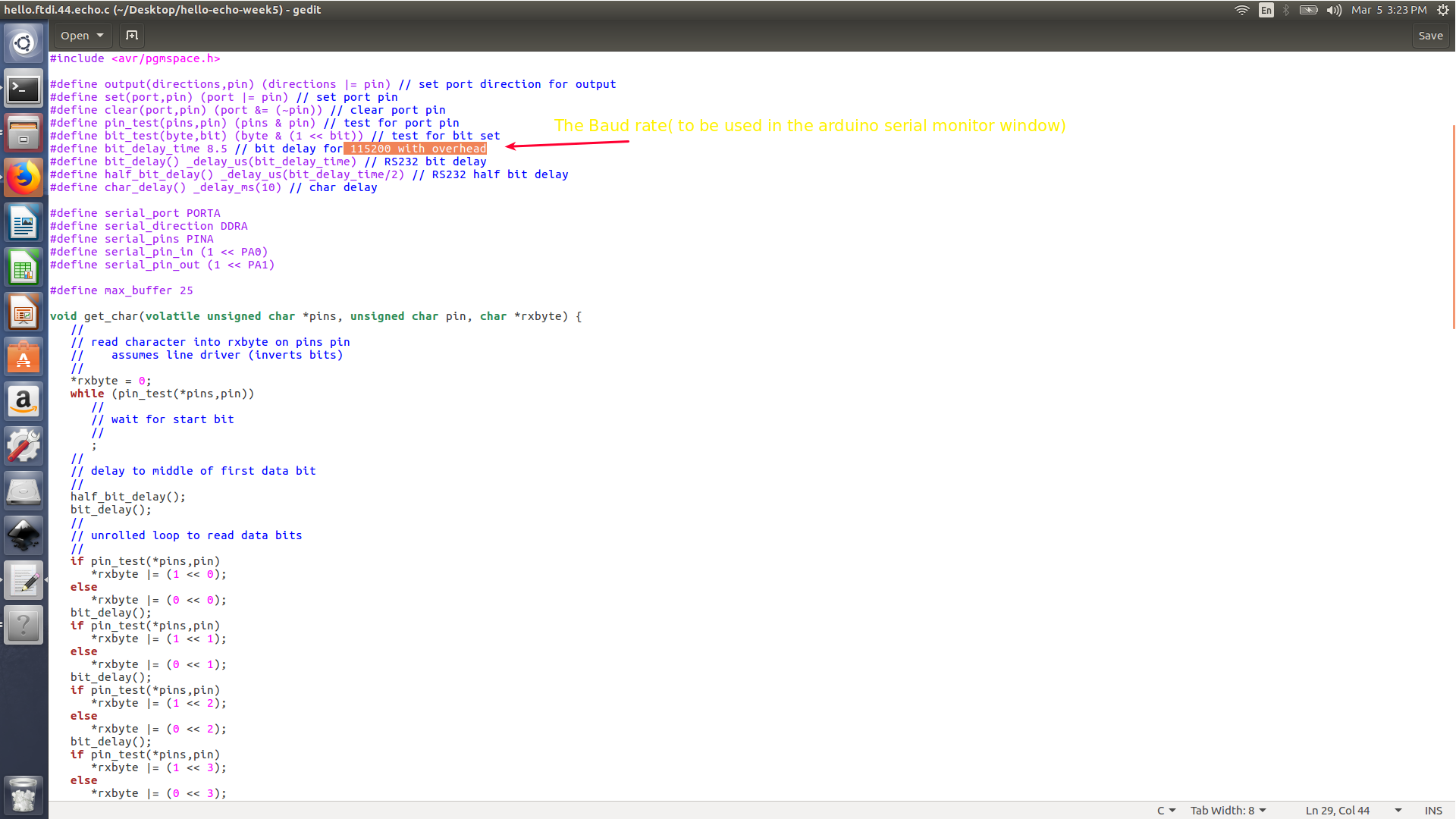
To ensure that the board is working properly, we had to test a serial monitor program on it (already written by Mr.Neil) link were I downloaded the hello.ftdi.44.echo.c (C file) and hello.ftdi.44.echo.c.make (make file). One issue that encountered us was once we type in the terminal make program to change the C file into hex, it was given error so we had to change the make file name to (Makefile). I run make program-usbtiny then run make program-usbtiny-fuses
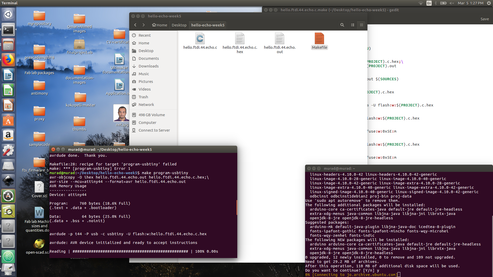
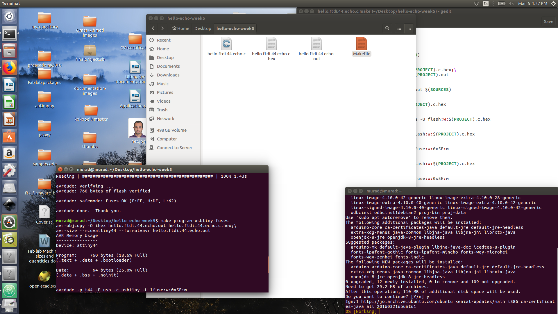
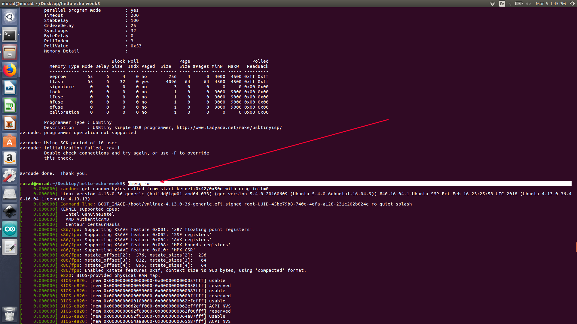
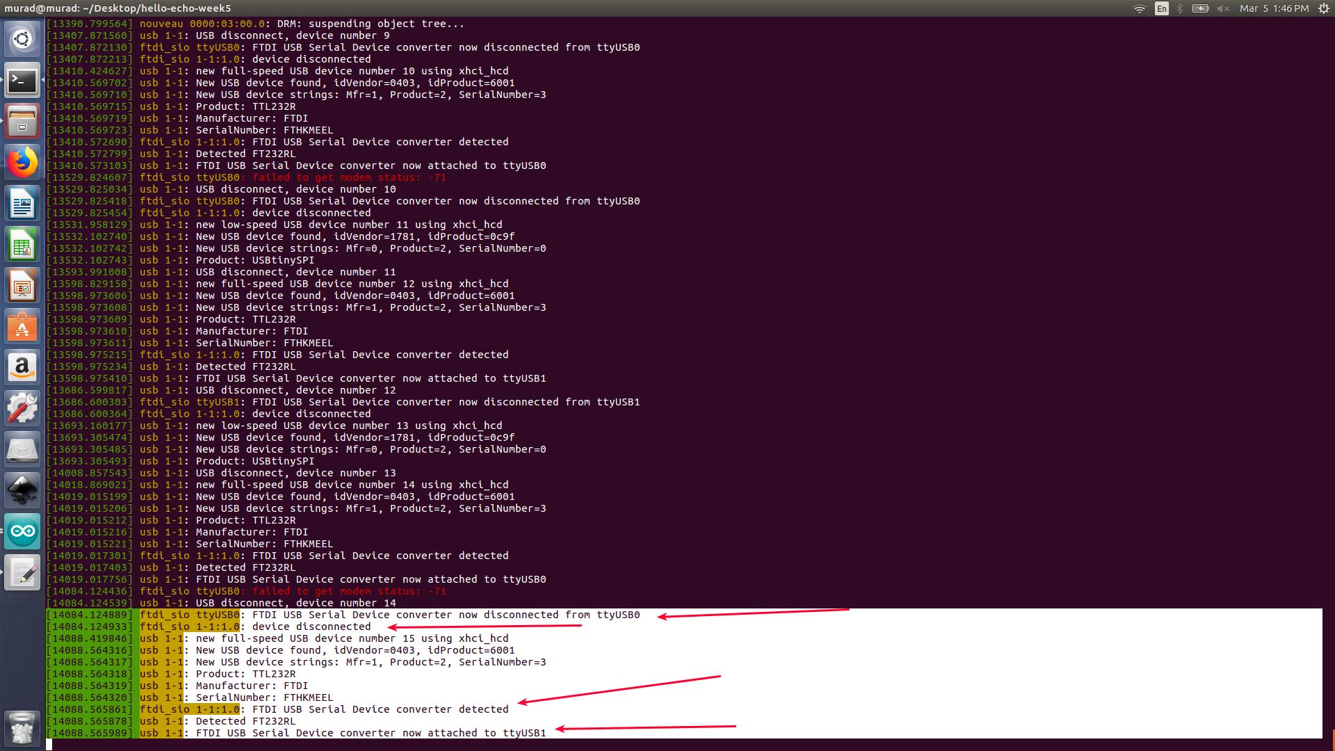
To check if you micro-controller is connected to your laptop, run dmseg -w to watch activities.
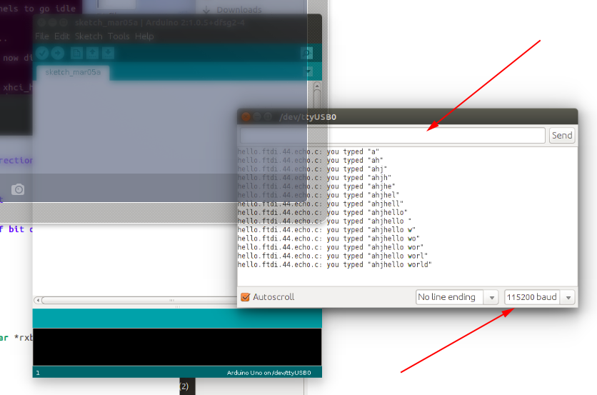
To test the board we have downloaded Arduino IDE and its serial monitor to send letter to our micro-controller. Once the serial monitor read stuff from our micro-controller this would mean that the micro-controller is working fine.
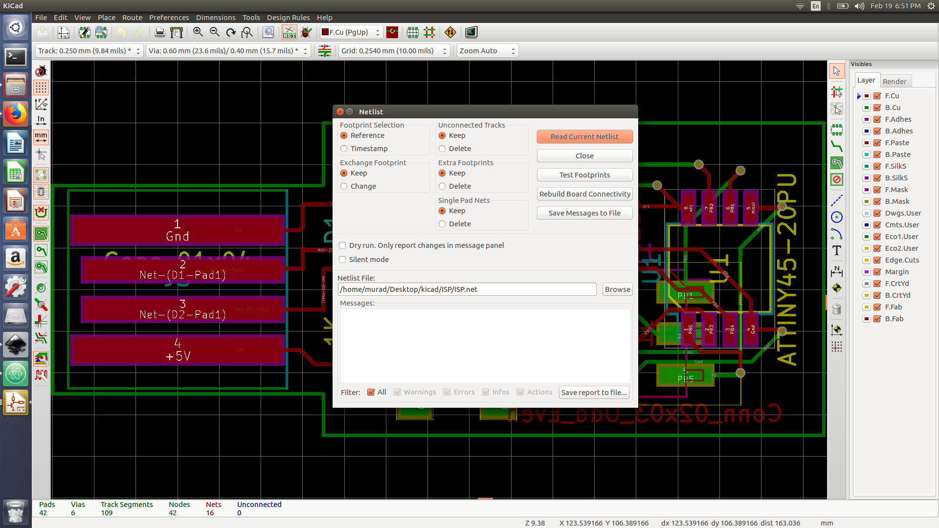
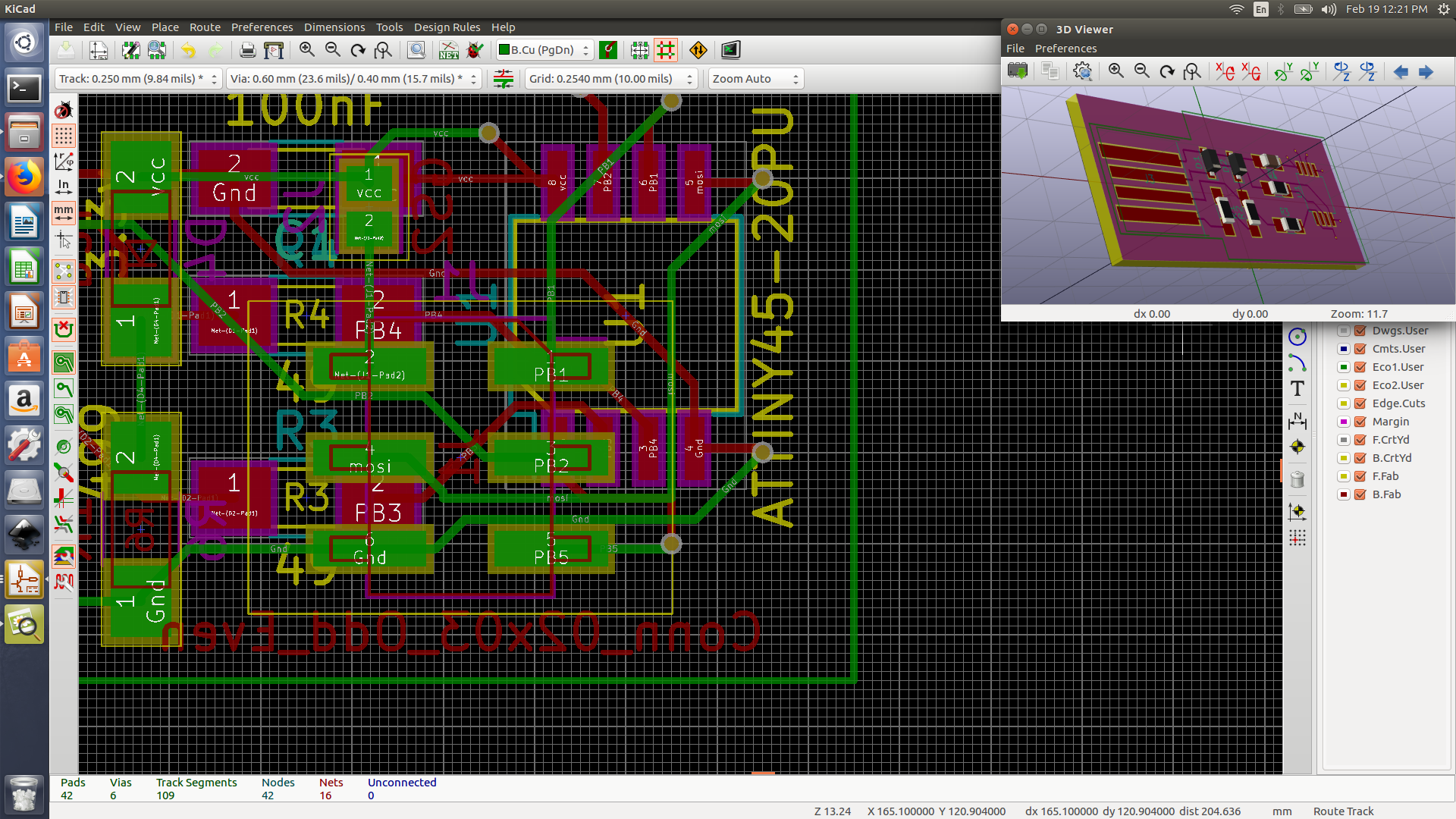
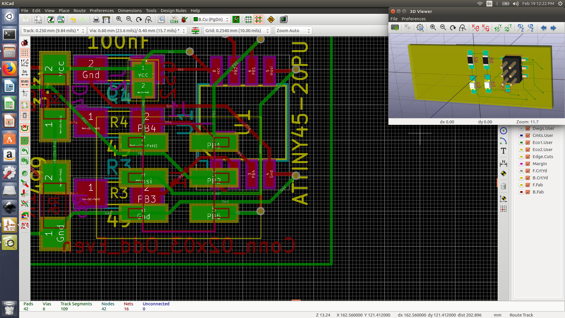
Ki-cad
I ll be referring back to my experience in ki-cad to design a double sided isp-tiny pcb during the 4th week assignment. Eagle and ki-cad are very similar, as both of them have a similar work flow, however ki-cad allow user to create their own component, moving a route would not also move the component, the ability to 3d view your pcb and allow you to create 23 pcb layers for free, on the other side eagle interface is simple and kinda straight forward , design can be exported as image (PNG format), but the number of layers is limited to 2 free layers only.
Source files
download fileKokopelli button-led board
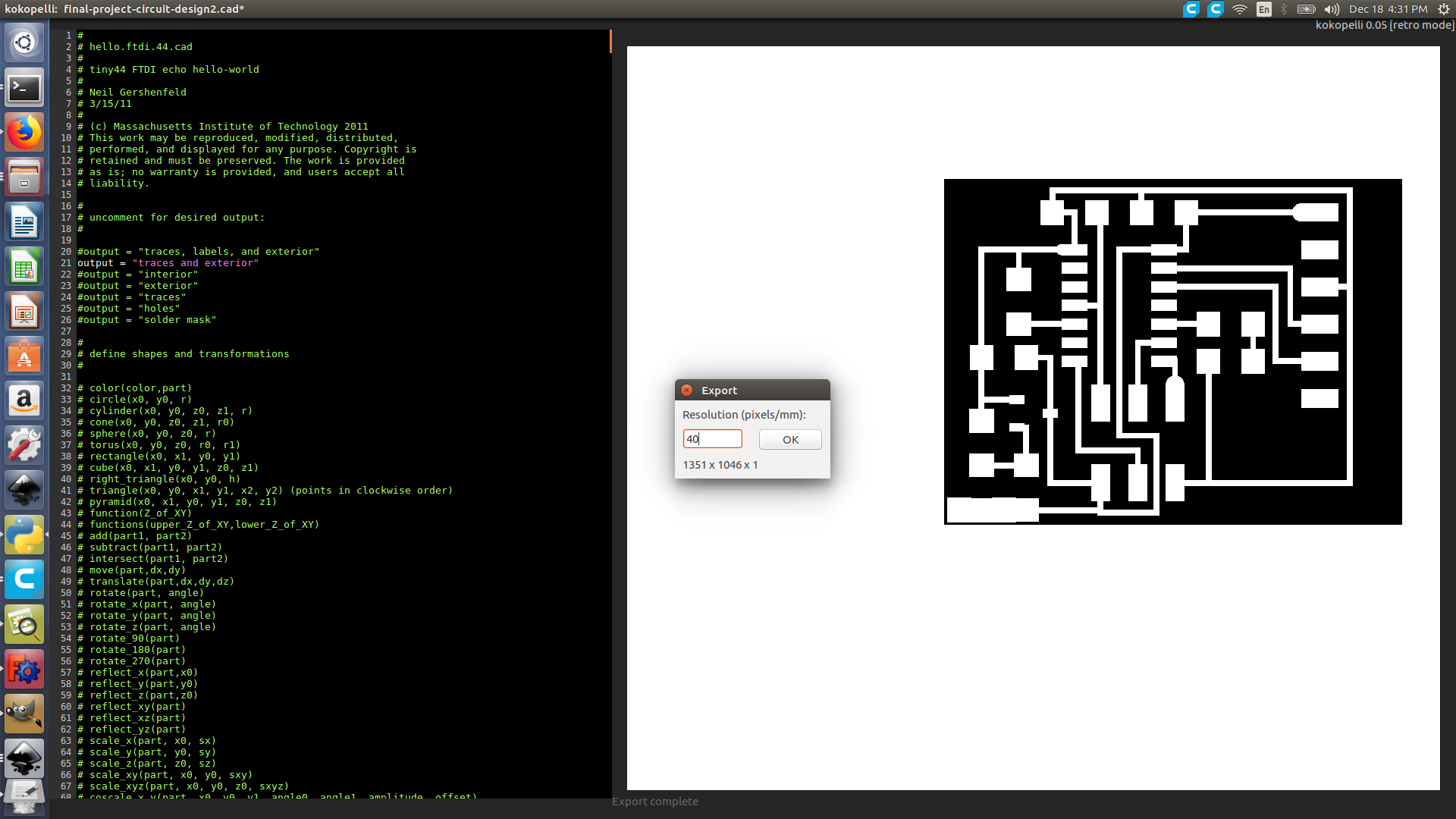
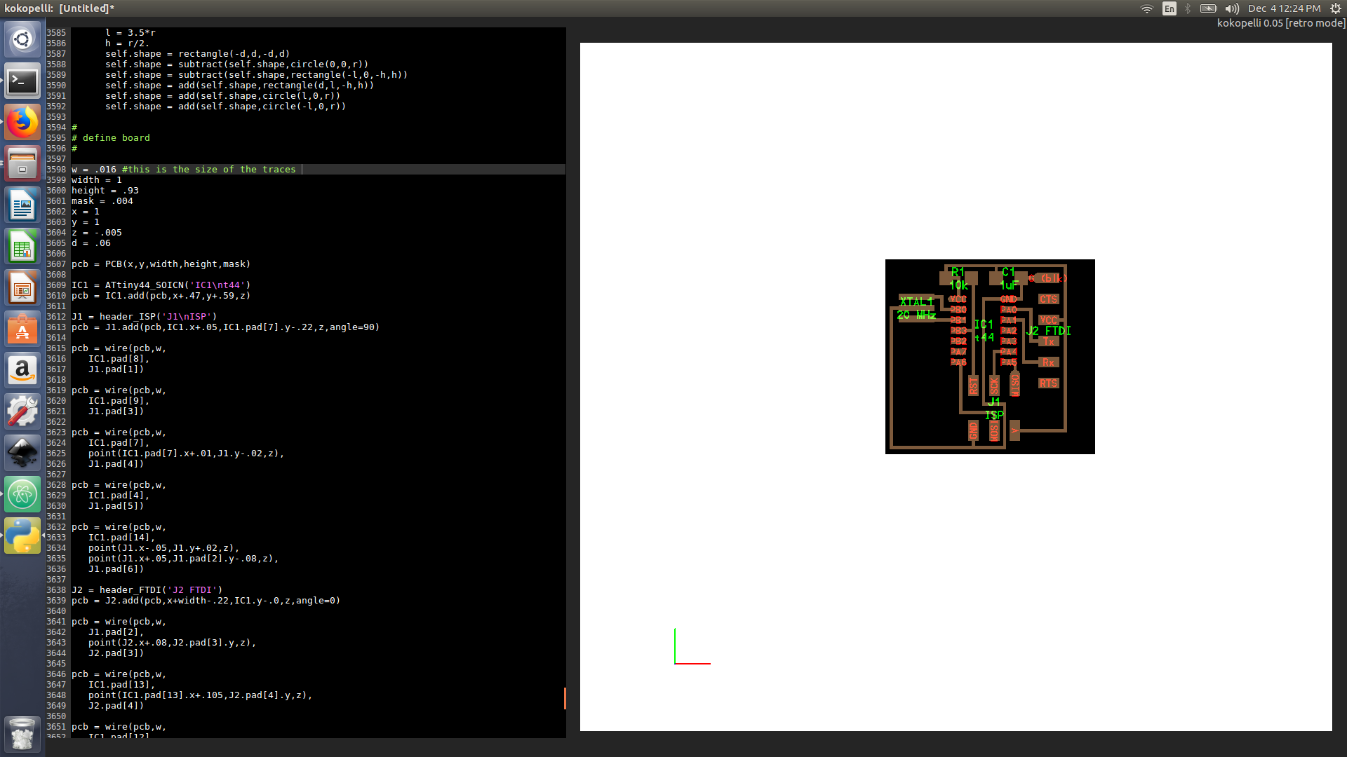
During my pre-fab academy I have used kokopelli to add a LED and button to an existing Attiny 44 micro-controller board.Kokopelli is a software tool for computer aided design and manufacturing. It uses Python script language to design circuit boards. the software contain libraries that defines various shapes and object, moreover you can design your own shape and objects and add them to libraries. Mr. Neil has plenty of electronic component defined thus we used aa tiny 44 cad file to re-design our LED-Button circuit.
To download Kokopelli:
- Download the zip file from the following link Kokopelli.
- open the terminal after extracting the file
- Type
make fab - then open the terminal from the bin file
- Type
./kokopelli -rand the software will start running
Desinging LED-Button PCB:
-
We copied the aatiny 44 Niel’s cad file and paste it at Kokopelli
-
We connected the button between PB2 and GND ( object used button_6mm)
-
We moved the traces a bit to give space to place the LED
-
We placed the LED between PA3 and Vcc
- We could not find LED defined in Neil’s code, thus as it is similar in size to the 1206 resistor we used resistor_1206 object to replace LED
-
Save it with a file extension .cad
- Remove the comment at the beginning+ of the code for output = traces and exterior
- Then export the PCB design as png image in order to cut it using SRM-20 machine ( ensure to set the resolution to 40 which is 1000 dpi )
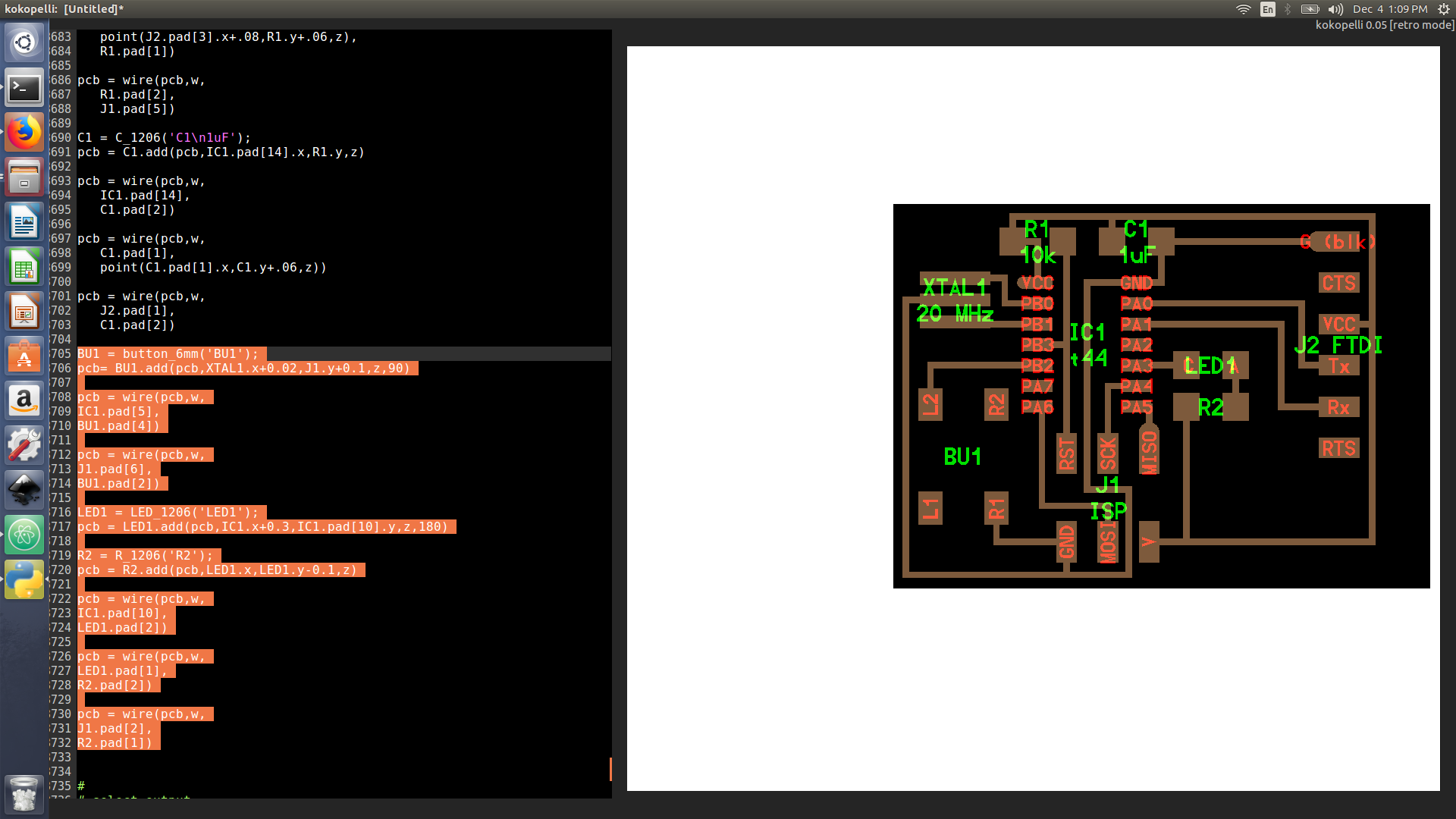
Kokopelli is a very powerful tool, however its very time consuming compared to eagle and ki-cad. As it requires the user to type all the connection and component by manually typing code. It's okay for such a small circuit but as the circuit gets more complicated, it would be kinda tough.