Electronic production
I have already created a tiny ISP during my pre-fab academy, thus I ll work on creating a double sided one with less area size. I ll first add my previous per-Fab Academy documentation and then I ll write about my experience in designing a double sided ISP tiny.
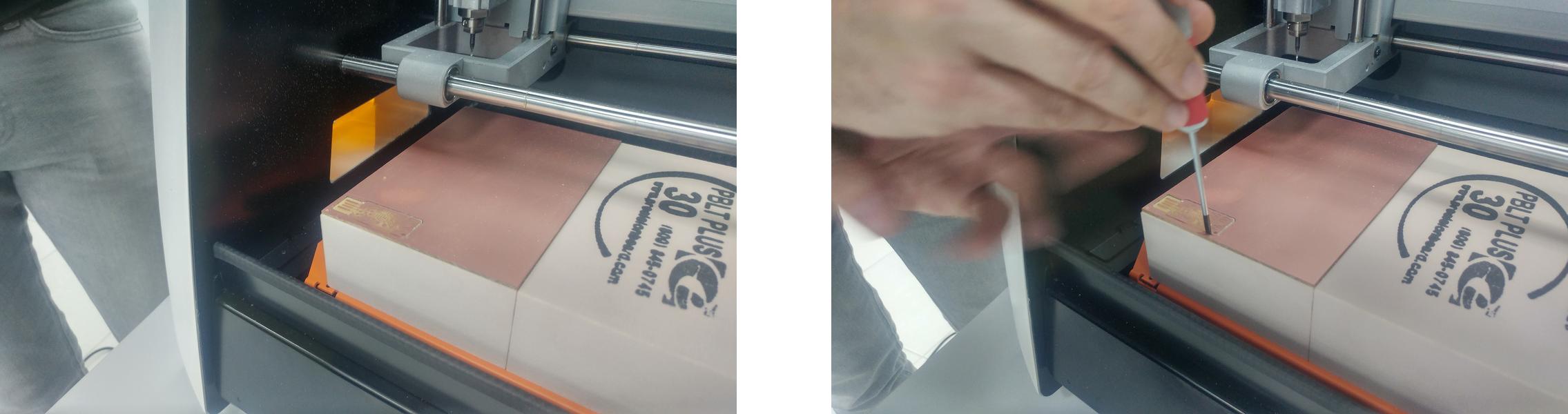
Roland SRM 20 (mono fab )is used to print and cut PCB.
Setting up Roland SRM 20:
- A corian material( or pad) to be placed above the machine plate, as the machine machine maximum low point is very high and wont reach the board
- Double tape the pad and stick in the printer
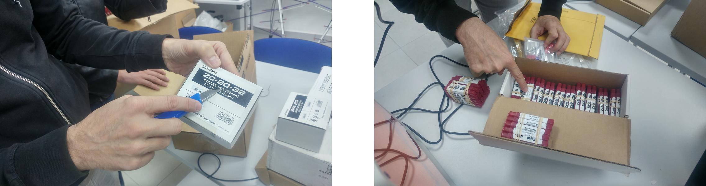
- machine has two types of spindles either the 3.1755 mm and 6.33 mm
- 1/46 inch milling bit is used to cut the PCB trace ( handle with care )
- 1/32 inch milling bit is used to cut the board and the vias
- The two milling bits we used have two flutes (sharp edges)
- The board applicable for the Rolland mono fab is the FR1 board ( made out of paper)
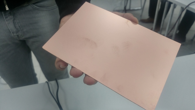
- Always hold the PCB board from the side ( not to rust the copper)
- ** Never use the FR4 board for this printer as those boards are made out of glass and epoxy**
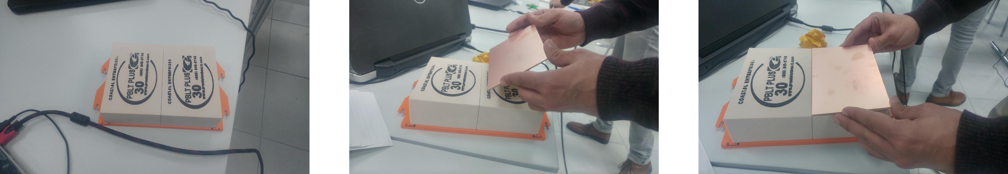
- To cut a two sided board, The board should be symmetric
-
Place double tape on the PCB before setting it in the printer
Fabricating Fab Tiny ISP (programmable board) :
- Download the PCB trace and outline images from Brayan electronic production documentation
- upload the PCB image to the fab model website [Fab modules]
- Choose the input to be image.png
- Choose the output to be Roland mill (.rml)
- Process: choose PCB traces 1/64 inch to cut traces and 1/32 inch to cut the outer board
- set x0= 0mm, y0= omm, z0= 0mm [Setting the origin]
- set the cut depth= 0.1mm for traces and 0.4mm for the board ( should be half the milling bit)
- set number of ofset= 4 for traces and 0.1 for the board
- set the input dpi= 1500
- Save it (Do not send it)
- Download the machine software Roland mono fab (* only for windows*)
- Access this link [Roland software]
- Follow the instruction
- Run the V pannel software for the SRM-20 printer
- From the machine coordinates Choose the origin to x= 2mm, y= 2mm and z= -33mm ( never use continue command to reach the z level)
- Release the milling bit to set on the board then lock it
- Click on the user guide and Set this as the new origin
- Press cut
- Choose the file
- Press output ( the machine will start printing )
- Carefully remove the PCB using a screwdriver
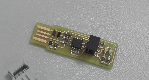
Components
- 1x ATtiny45 or ATtiny85
- 2x 1k ohms resistors
- 2x 499 ohms resistors
- 2x 49 ohms resistors
- 2x 3.3v zener diodes
- 1x red LED
- 1x green LED
- 1x 100nF capacitor
- 1x 2x3 pin header
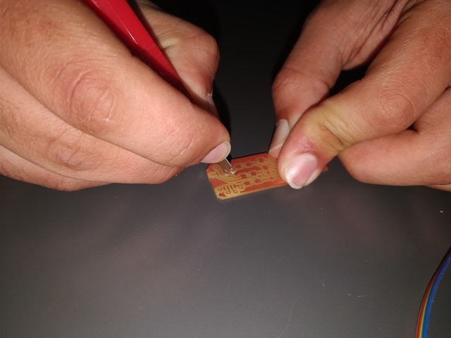
Soldering the components to the board
I have found this video very useful which shows different techniques for soldering SMD components Soldering Youtube tutorial
- Pick up the soldering iron in one hand, and the solder in the other, as per the picture below.
- Use the soldering iron to heat up the pad for 3-5 seconds, not the pin on the component.
- While the pin is hot, position the solder between the pad and the pin. The heat will melt the solder, and the flux will cause it to flow where it needs to.
- Use tweezers to place the component
- Heat up the other pad side and then apply solder
- keep the fume absorber always on while soldering as the smoke which contain LID could affect you badly.
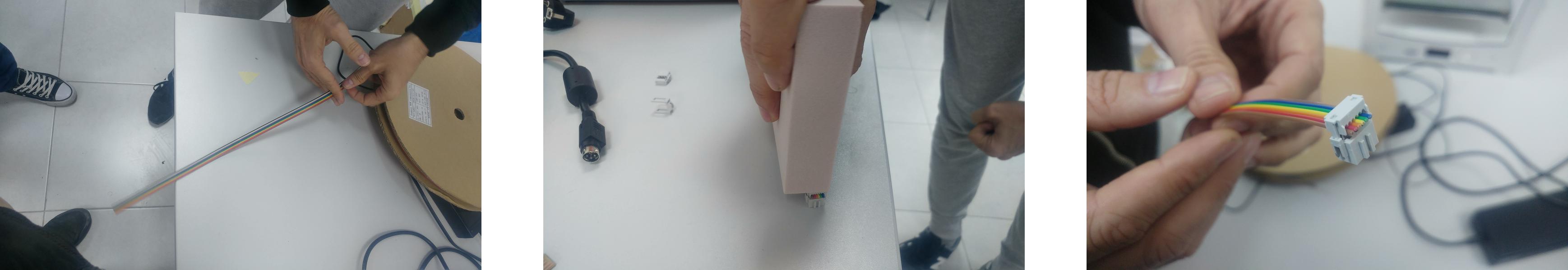
Programming the board
- Install the development environment software
sudo apt install avrdude gcc -avr avr lilbc make - Get and build the firmware
- Open terminal at the extracted file location and run
maketo notice that a hex file has been added - If your are not using another usb tiny to program your usb, ensure to open the hex file and amend PROGRAMMER ?= usbtiny to PROGRAMMER ?= atmelice for the white box programmer
- The red LED should be lit up
- Ensure that the programmer is correctly connected to pin 1 in the right place
- In the terminal Run
make flashthis will erase the chip and program its flash memory with the contents of the .hex file - Now run
make fusesthis will set up all of the fuses - Test the usb functionality by plugging your board to the usb port and then run
lsusbif you see a “Multiple Vendors USBtiny†device. Everything is working perfectly
 Your ISP tiny is ready to program boards now
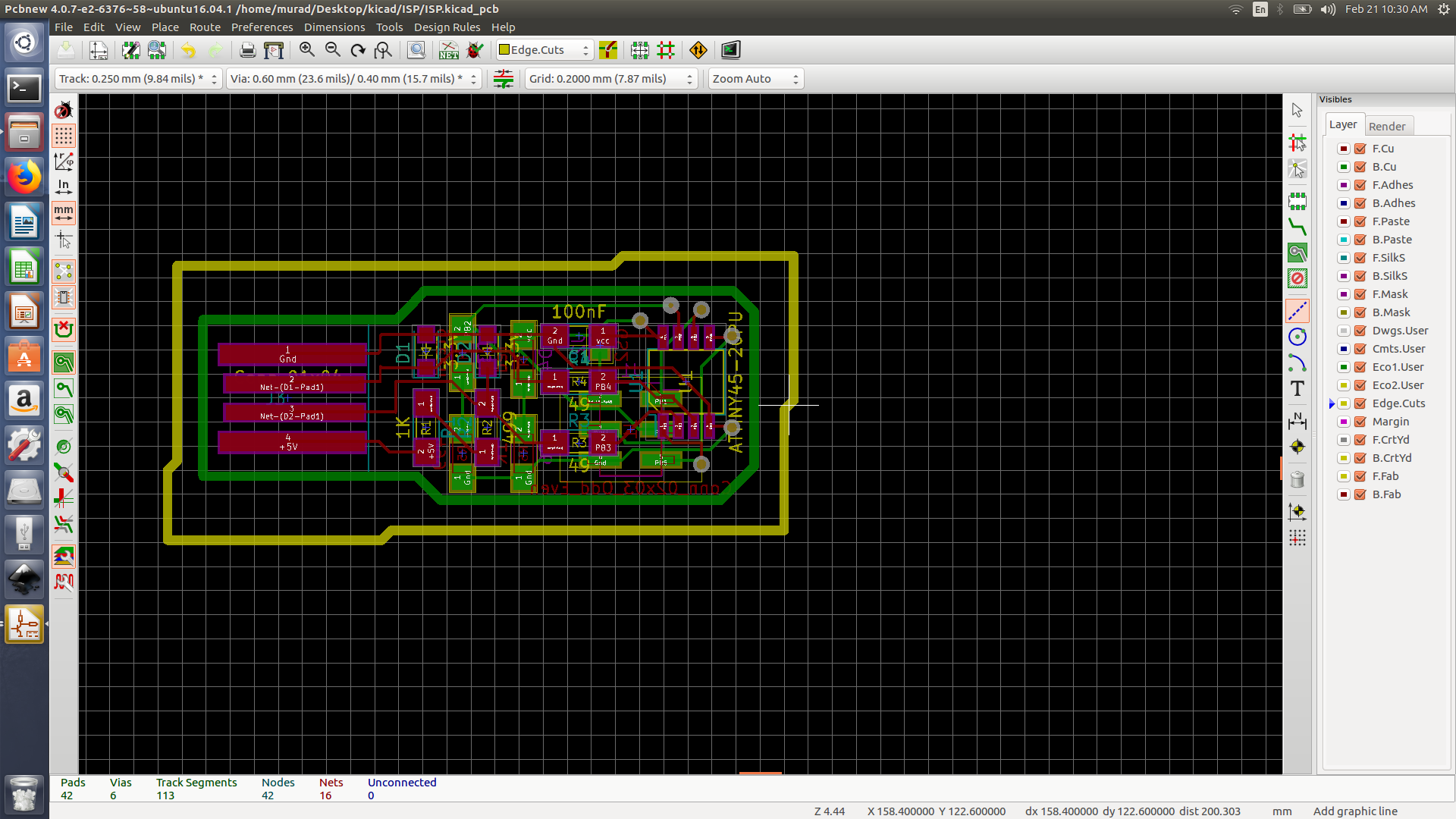
Double-sided ISP-tiny
I wanted to experience how print a double sided PCB so I decided to modify the current ISP tiny, I used Brayan documentation as a reference. At the begging I was searching for the best tool to design a PCB. I have downloaded Eagle and Kicad. I was honestly looking for a simple PCB design interface without the need to have a schematic diagram ( something like Kokopelli). I decided to use Kicad, I have created the schematic diagram and then moved to the PCB design.
Note:
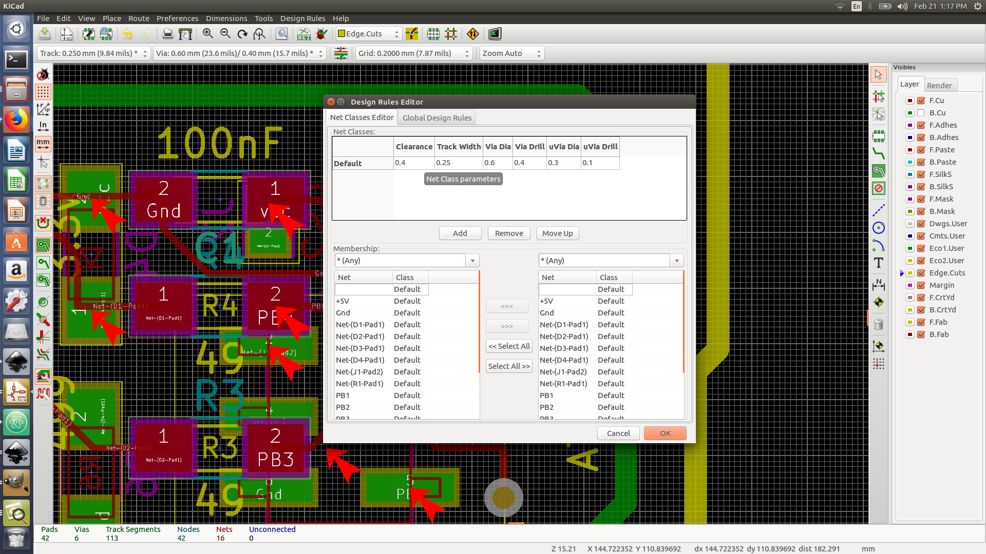
- Adding a global labeler makes your schematic diagram simple
- Always Annotate then run CvPCB foot print and make sure you choose the right component
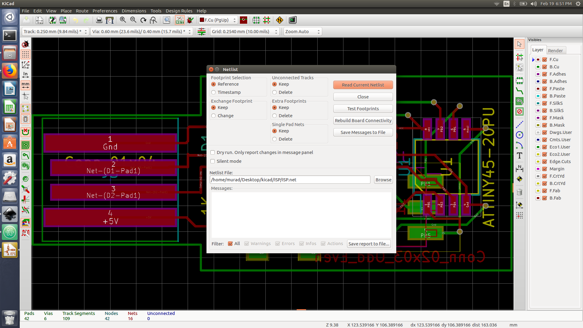
- Create a net-list
- Go to PCB editor and choose net list and read from the net list ( I have faced a problem as our instructor sibu has created the USB_A footprint as it wasnt available and I had added it to the schematic but not to the main file) so I just copied it and read it from the library and all the foot print were available at the PCB editor.
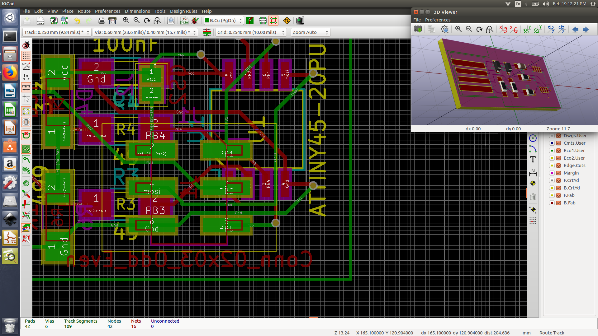
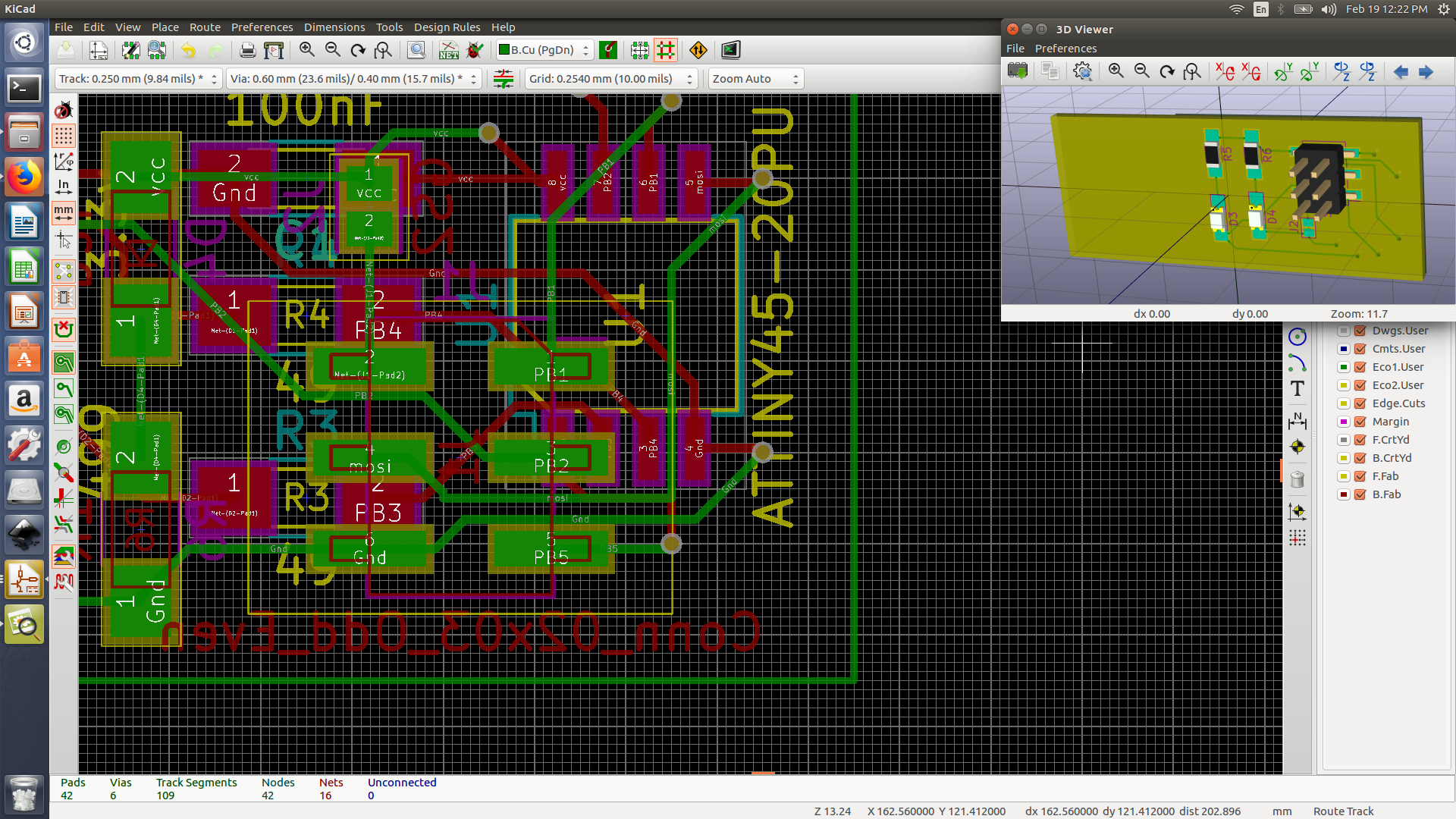
- Switching the view from canvas to open GL gives you a lot of flexibility and options ( for example the auto-routing work best in this view)
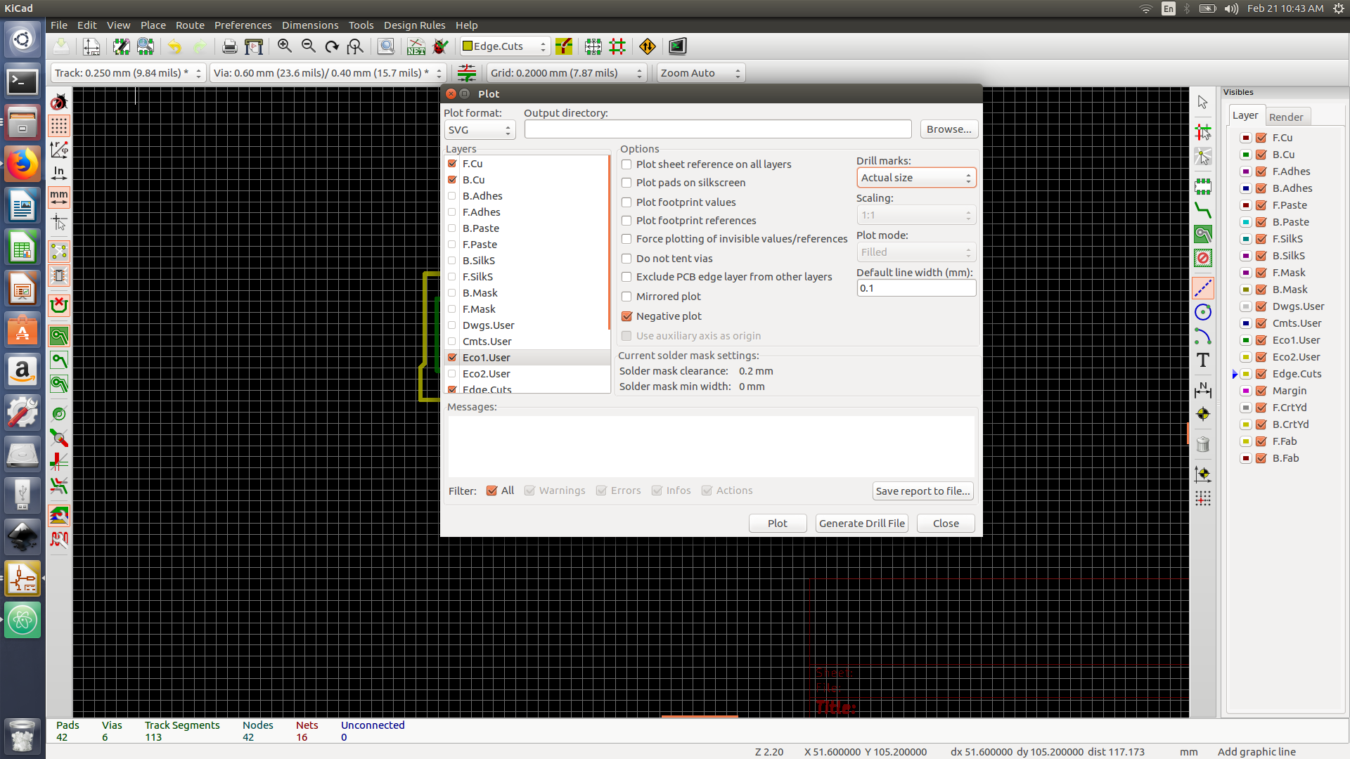
- I exported the PCB design as a SVG file (actually its better to do it using plot, make sure to tick negative plot)
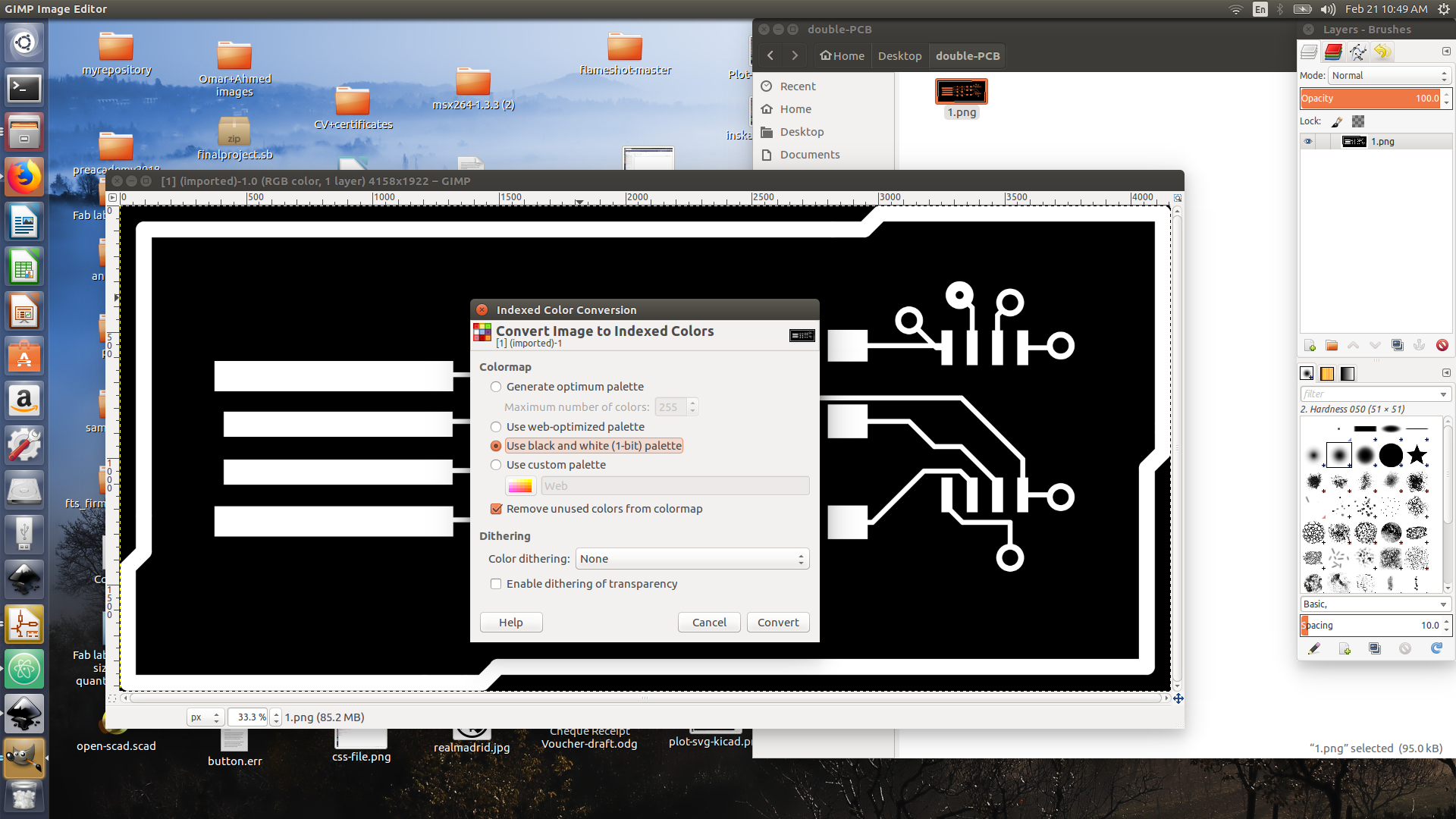
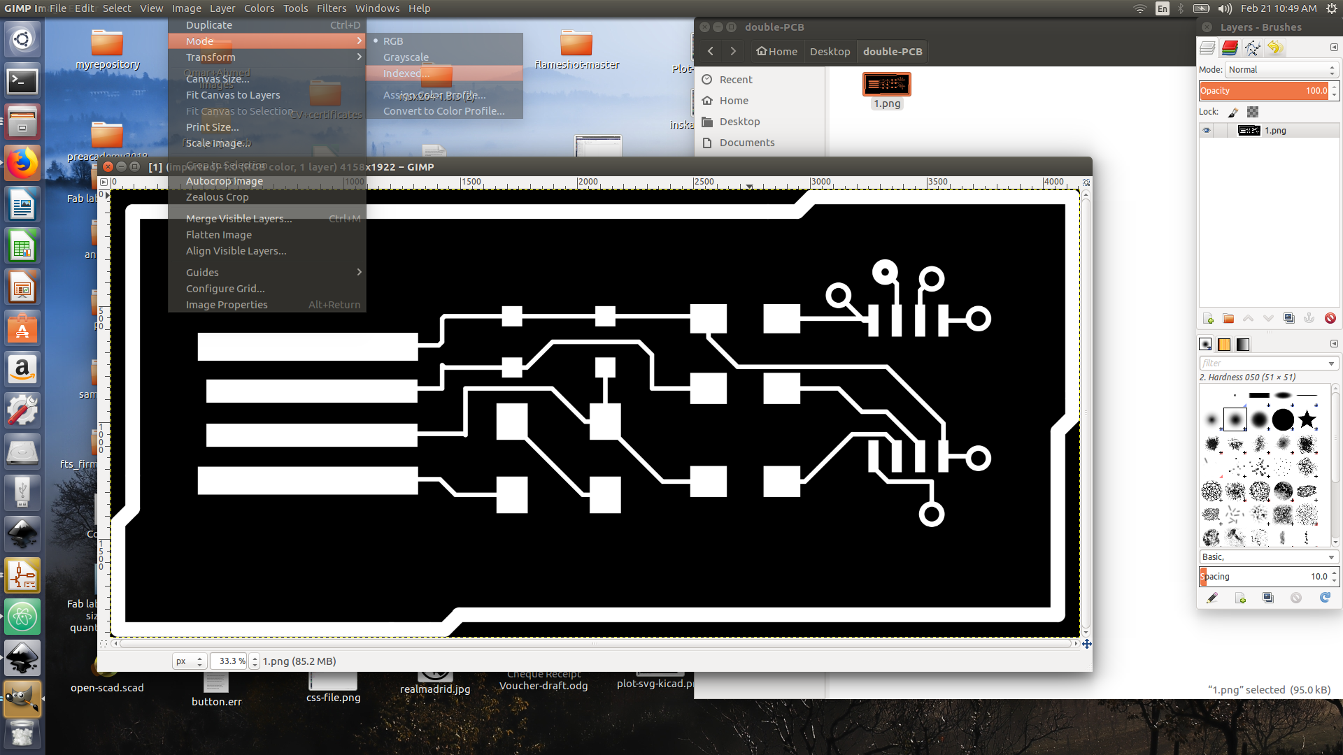
- I ll edit it using inkscape to convert it to png.

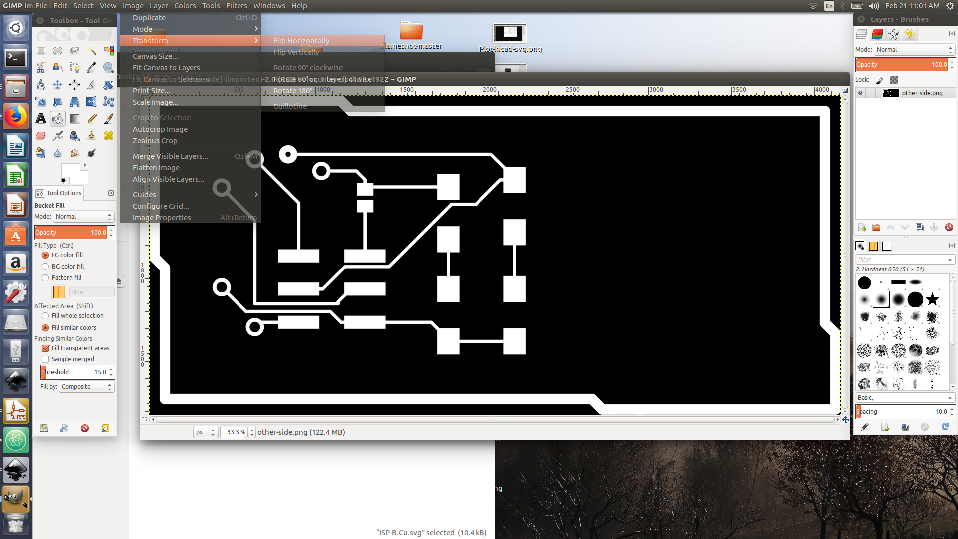
Cutting the double sided pcb
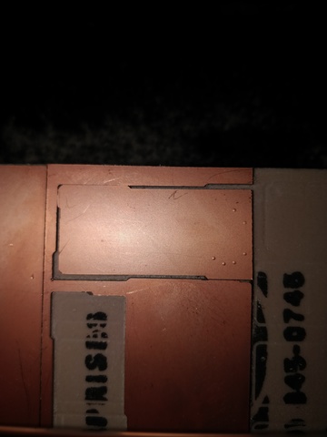
I thought cutting a double sided pcb would just require us to cut the first side and then just flip it and cut the other side, however we ll have to cut the traces of the first side then flip the entire pcb board and cut the second side and then cut our PCB board. This will require a precision in flipping the board and where to exactly cut the second board. Our instructor Sibu came out with an intelligent idea on how to cut a double sided PCB that would ease the flipping method of the pcb while making sure its on the same origin, this is difficult as once the PCB is cut replacing it will keep a 0.8 mm (which is the cut bit diameter 1/32 inch) space to it to move which could cause a misplacement. Sibu came up with the idea to place tabs on the outer cut layer, this layer is rectangular in shape to allow the pcb to be placed again perfectly. For more information visit Sibu’s page (Link)[]
Issue faced:
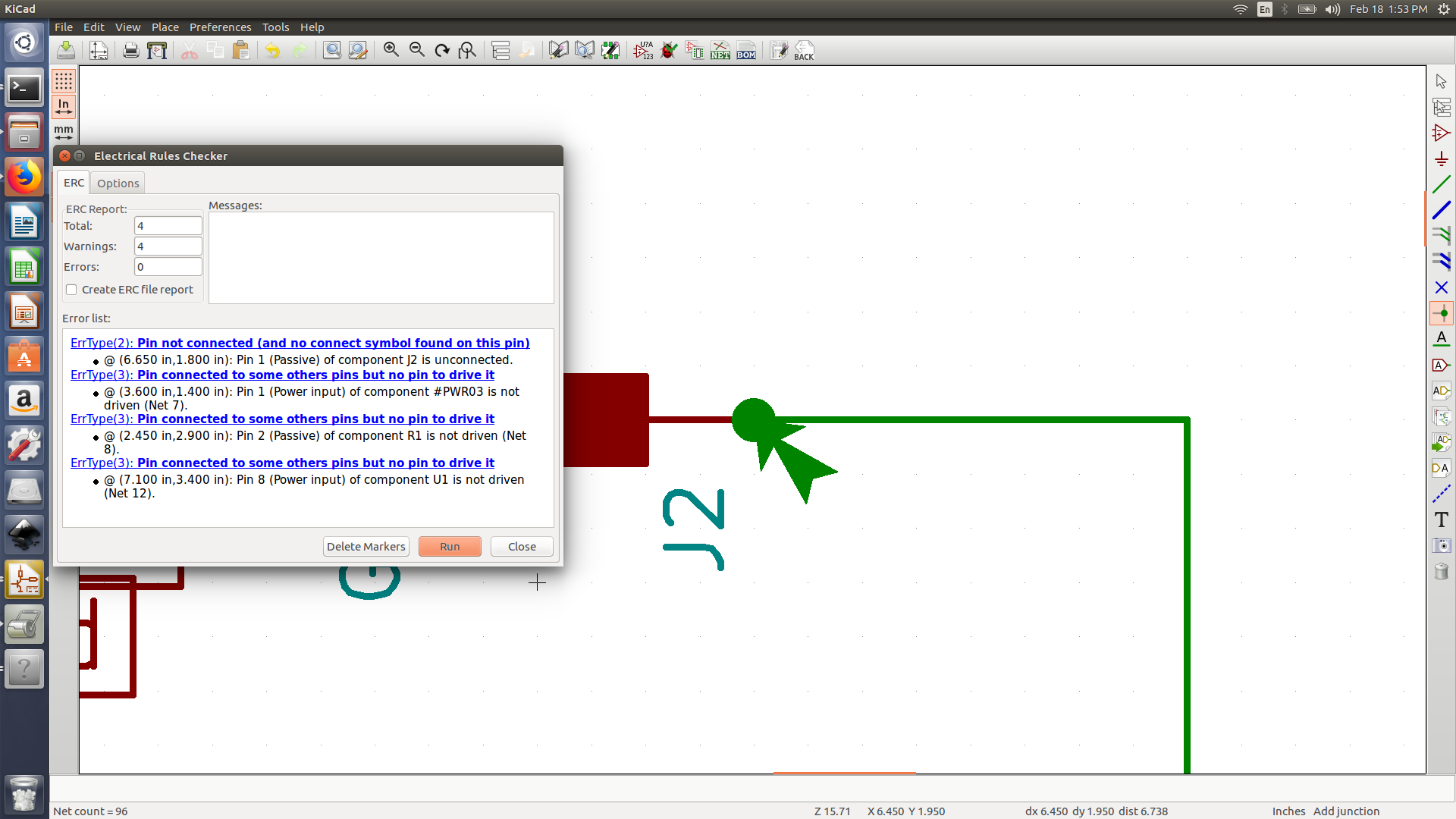
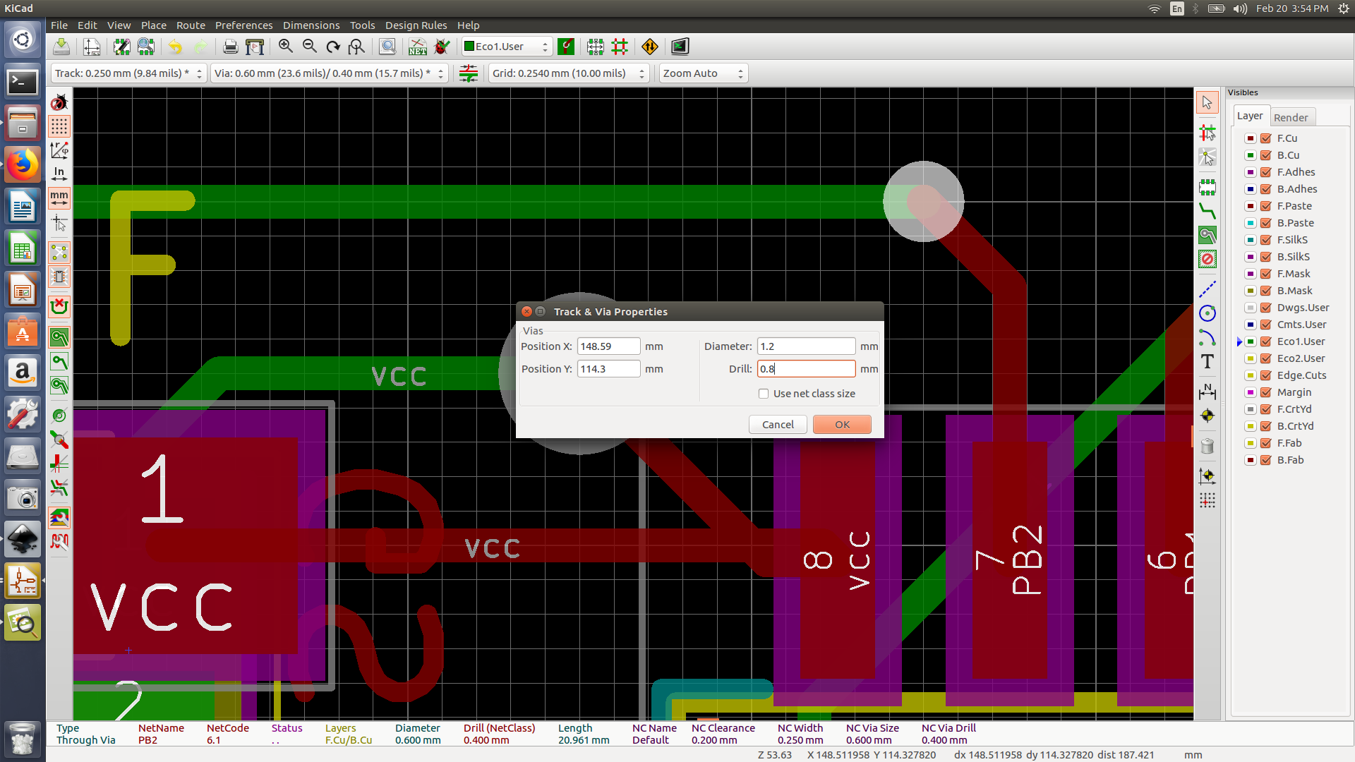
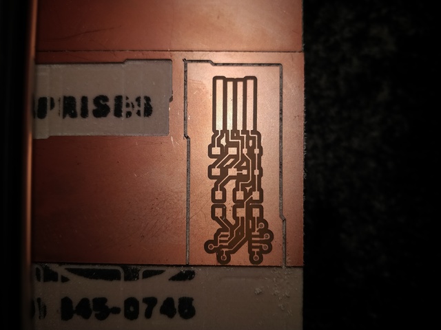
- I had to increase my via diameter to 1.4 and 0.8 for drill according to 1/32 cut bit.
- Some traces were intersecting after i printed my pcb, I should increase the distance between them to 0.4 and then test it using run drc. As a temp solution I ll cut them manually ( check the last image).
- do not move anything in ikscape after plotting
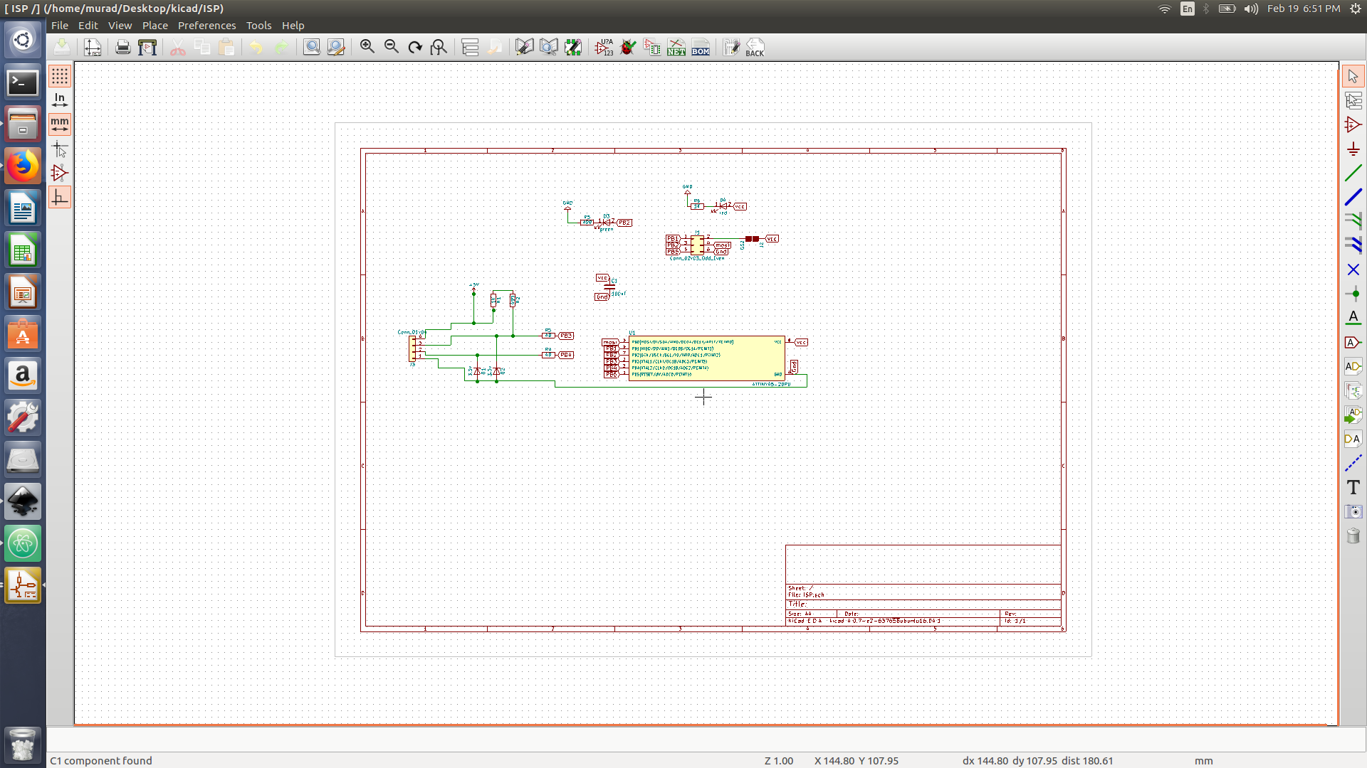
Programming the ISP tiny using Arduino
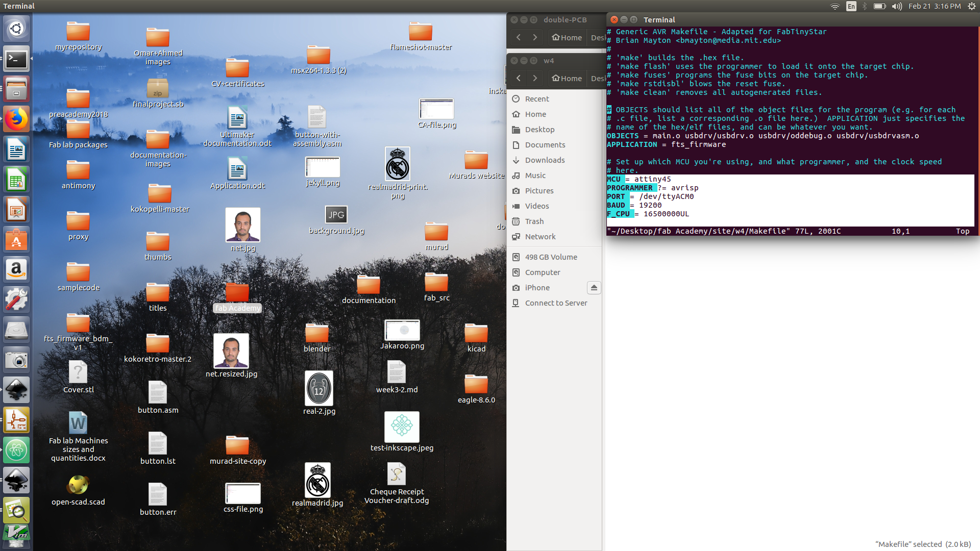
You can learn more about that by accessing our tech work fab lab website. Please ensure to connect the Isp tiny to the arduino correctly and then just edit the make file as in the image below