WEEK 6 - ELECTRONICS-DESIGN
Assignment - redraw the echo hello-world board,
add (at least) a button and LED (with current-limiting resistor)
check the design rules, make it, and test it
extra credit: measure its operation
extra extra credit: simulate its operation
Here is the link to Group assignment.
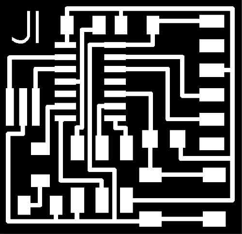
REDRAW the echo hello-world board
eagle
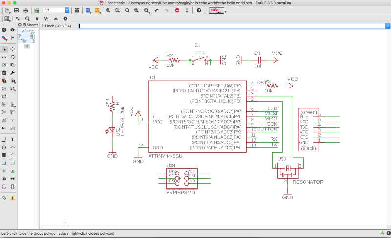
First, I tried to use the board design program from Autodesk, Eagle. I downloaded the program and make a license as a student. And, followed the tutorials. I downloaded library file from class page. And, I moved that file from download folder to library folder which is located in application/EAGLE-8.6.0/lbr
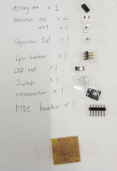
This lbr file has all the components that used in fabacademy and also components in our fablab inventories. As I moved the library file to program, I can load and use those components in eagle. I launched eagle and make new project, I named hello.echo.world. And create schematic file, there is nothing on the window. I put add button and load every single component. Components are ATTiny44, three resister, capacitor, 6pin header, LED, tactile switch, resonator, FTDI header. I loaded every parts and name and put values. Resisters were 499 Ohms and 10K Ohms. resonator was 20.0mHz. Capacitor was 1uf. After putting every name and value, I put vcc and gnd as components rather than connect every components. I grouped LED and current limiting resistor. And to connect without net, I put every name on pins like RST, MOSI, MISO, SCK etc.
• SCLK: Serial Clock (output from master).
• MOSI: Master Output Slave Input, or Master Out Slave In (data output from master).
• MISO: Master Input Slave Output, or Master In Slave Out (data output from slave).
• VCC: Positive supply voltage.
• GND: Ground.
• RST: Reset.
If I put name on it, program asks for connect. Then I approved. After I connect every components, I organized all parts to find out easily. Then, I was ready to make a board to make milling.
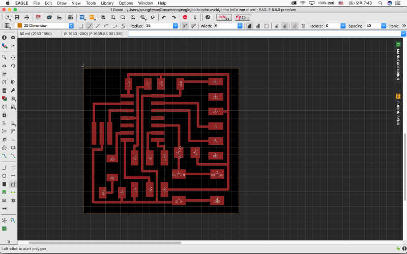
I created board file and saved at my local directory. I want to make my board compact. So I searched other student’s assignment and tutorials. I found some design rules about vcc and gnd go around the board is easy to connect every parts. And it’s easy to connect SSU and headers when there is no other components between them.
This is the tutorial I referenced.tutorial.
I considered how to make compact and to make no problem when I solder. I put every components near and created routes. Drawing routes, board became bigger and bigger. So I tried to find any routes can pass under the components and drew. Every processes while drawing and making compact were draw the routes, move components, modified intervals and repeat these processes.
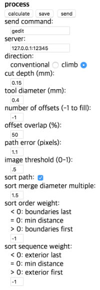
Before I checked design rules, I put 16mil on every values on clearance menu in DRC(design rule check).
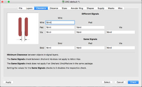
And checked design rules. It said there were several errors about airwire and clearance. Airwires were picky problem that said each routes weren’t connect to components. Routes were on the components but those were not connect to components’ center called airwire. I don’t want to see those error messages. So I rearranged all of those part. Then, about clearance, those parts were too narrow to endmill go between two routes. So I modified interval more than 16mil. And almost exactly 3 routes could go through under SSU.
MILLING
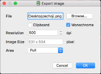
Then I exported the board file to make png file. I push the export button and select image. And checked monochrome and put resolution value. But I noticed size of image changed according to resolution. I couldn’t understand about this changes because components sizes are fixed. Then, I put 500dpi as a resolution following tutorial.
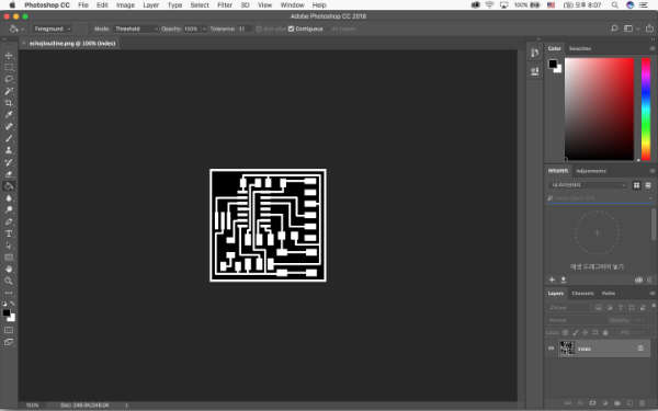
I saved png file and opened on Photoshop to make an outline file.
I opened it and cropped the edge of trace file to make it smaller. And I tried to offset to make interior file. But I noticed image size was about 5cm height and width. Something wrong. I checked pixel size and it was almost 2 times than I expected. So I didn’t save the file and reopen the png file. but it was same size. I think photoshop is not for the vector and it changes the file itself.
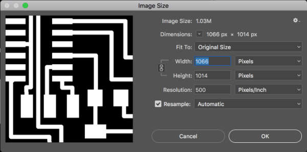
So I went back to export stage and captured the size of pixel when resolution is 500dpi. It was 531*505.
And I saved as png and open the file in photoshop. And I modified the image size. Then I got exact size.
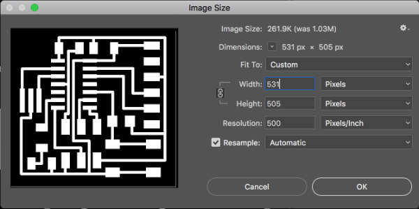
And I repeated crop, it became 490*474.
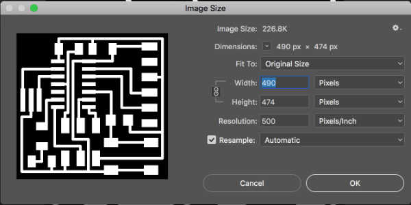
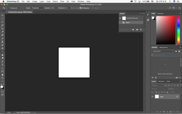
And I went to canvas size and offset 20pixels length and width, it became 510*494pixels.
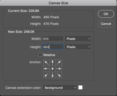
Image got white outline thickness 20pixels. I painted the outline black with paint bucket tool. And save as another file to make outline file. In this process, I put my first name on left top.
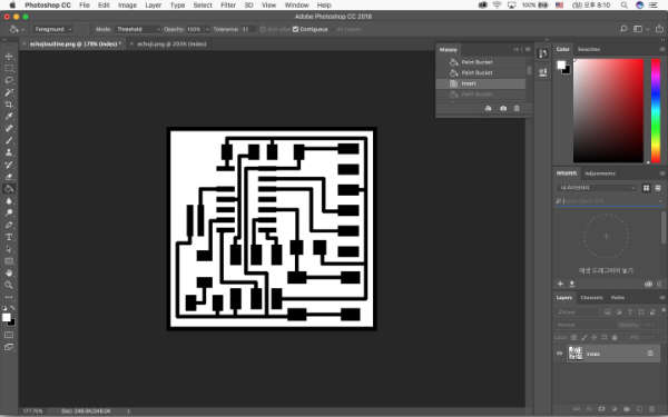
To make interior, I inverted the image that make black to white and white to black. Then, I paint traces to white. I got same sized trace png file and outline file.
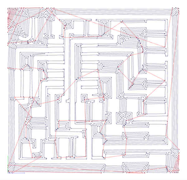
I loaded trace file on fabmodules and put every value like endmill speed and jog speed. And I put -1to make it clear to prevent shorts when I solder. Then I push calculate button, there was no problem. I saved file .nc.
I opened the file on bantam tool which is our milling machine bantam tool. I set the origin point on blank place and tool length and material thickness. Then milled the board.

And I created outline.nc file with thickness I probed before. And milled after trace done. It was fine. After milling done I removed the board from the machine bed and did some afterwork like clean with soap and sand surface with sanding paper. And remove useless tiny remain parts with cutting knife.
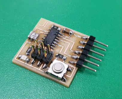
I arranged all the components and attached on the paper with tapes.
I soldered components considering soldering rules. In this process, I used different kinds of FR1 board to the board that I used when I made an ISP board. I felt it’s more tricky because copper sheet was easily tear when I heated the board for a while with pharynx. Even it was not that long. So there were two parts torn so I make connect with wire for one and connect with extra lead for another. And another problem was there was no enough place to solder resonator. I asked to instructor and get to know that I should solder every single corner so those were 6 in total. Also there was problem in LED, I made the pad short to make my board compact. But, there wasn’t enough pad to solder.
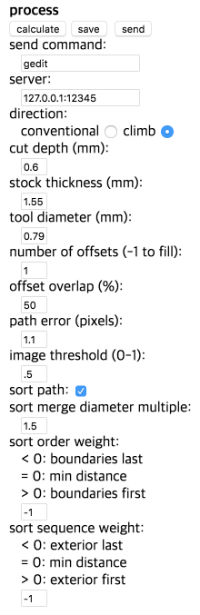
So I decided to make a board again. I open the trace png file on photoshop. I made it bigger to make easy on the pad, resonator and LED.


And I modified the thickness of the text because it was too thin I think. Same proceed with former. I created the .nc file and did the milling again.
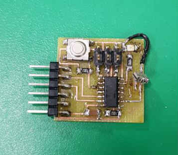
the board I used this time was same as the one I used to make ISPboard. Output was fine and solder was better too. In this proceed I desoldered the components as well as possible to reuse. I got every resisters, capacitor and resinator. I soldered components again and it was better this time. Then I have echo hello board.
BOARD PROGRAMMING
I also tried to program my echo hello board. I downloaded some files from class page.
Hello.ftdi.44.echo.asm.
Hello.ftdi.44.echo.asm.make
Hello.ftdi.44.echo.c.make
Hello.ftdi.44.echo.c
Hello.ftdi.44.echo.c.hex
Hello.ftdi.44.echo.interrupt.c
Hello.ftdi.44.echo.interrupt.c.make
Hello.ftdi.44.echo.out
And I created the folder named ‘hello’. I opened terminal and move to the directory hello.
And i connected my ISP board and echo hello board.
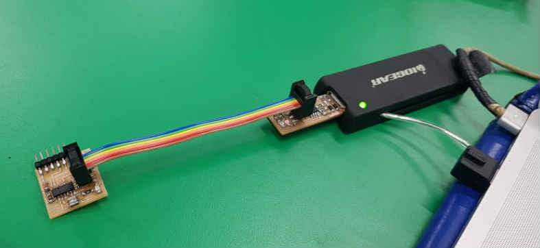
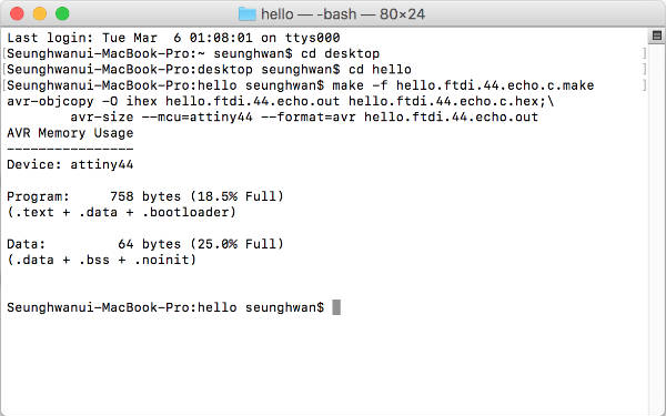
Following tutorial, I commanded to make from the makefile named ‘hello.ftdi.44.echo.c.make’. And the same messages from tutorial it was fine.
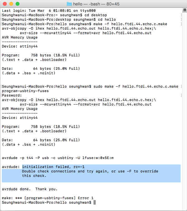
But on the next stage, I commanded ‘Sudo make -f hello.ftdi.44.echo.c.make program-usbtiny-fuses’ and it said ‘initialization failed’ and check the connection. So I checked every components with multimeter. But there was no problem. So I tried another ISP board from instructor but didn’t work. I can’t figure out yet.
PROBLEM SOLVING
Back to beginning, i checked the board and found problem. There was one part that cause short under ATtiny44. It was under the component so i couldn't find immediately.
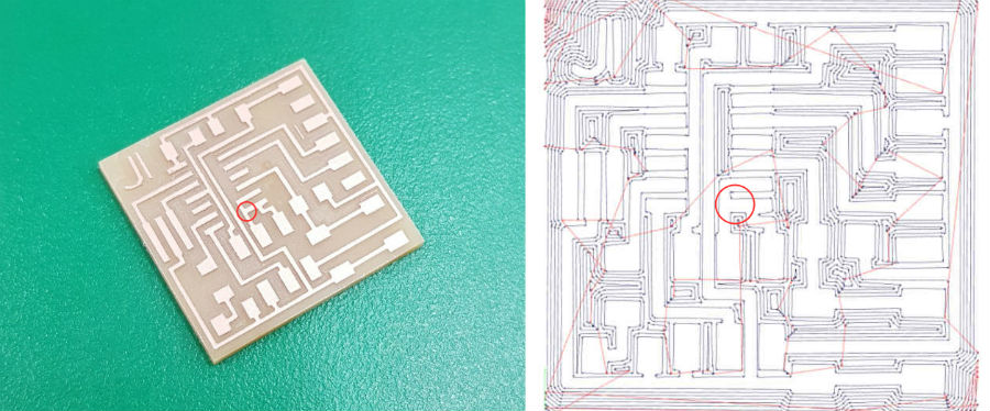
This part should be seperated, but at PNG file the gap between two part was too tiny so Fabmodule didn't create the path.
I desoldered ATTiny44 using solder wick and seperated two parts with cutter. Then, i resoldered ATTiny44 again.
Then programming was fine. Finally LED got blink!!
Here are my works.
Download