Electronic Design
Work to be done
- Select and use software for circuit board design
- Demostrate workflow used in circuit board design
Choosing a software
I will work with KiCAD software since it is well supported on the OS I use everyday(GNU/Linux). I also like that KiCAD is a free software, so it doesn't limit me on how big my circuit board can be.
I used KiCAD because I want to learn it more so I can continue to use it even after fabacademy for my personal work.
PCB design workflow
Designing PCB
I started designing the schematic of the circuit. As it was not my first time to work with KiCAD everything was fine.
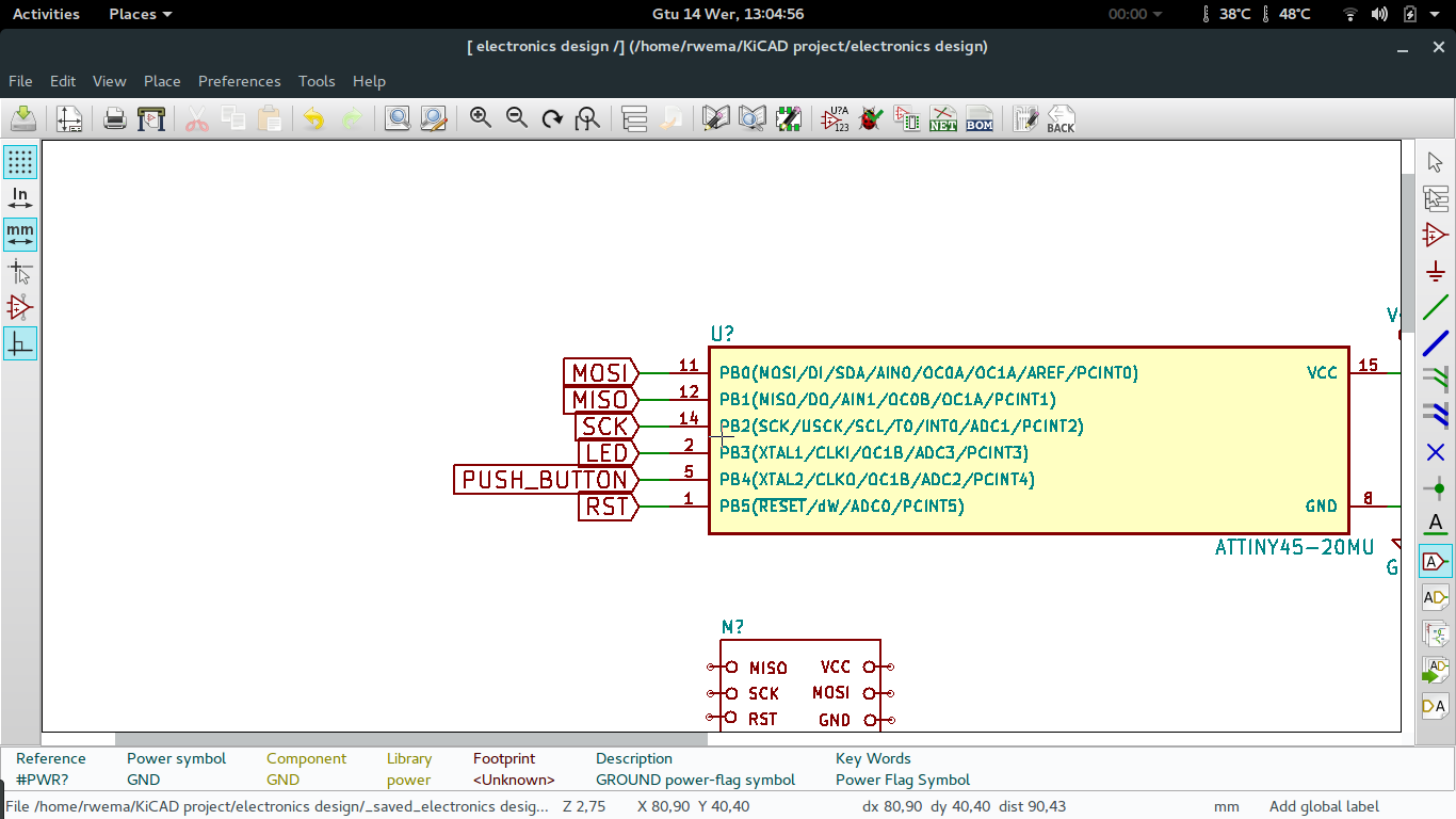
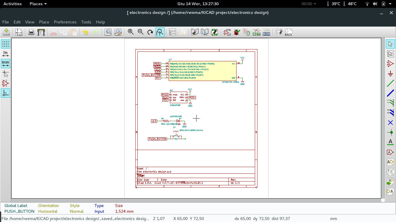
This was my final design of the schematic.
For me It was straight forward in designing the schematic because It was not the first time. If some one whose not familiar with KiCAD and other circuit design software looked at my designs would not understand the some of the software components I used in my design.
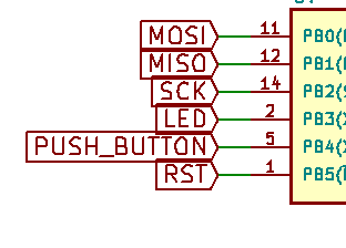
In brief these are the called global labels in KiCAD, are used in place of wires for making a clean schematic and easy to understand connection among different components.
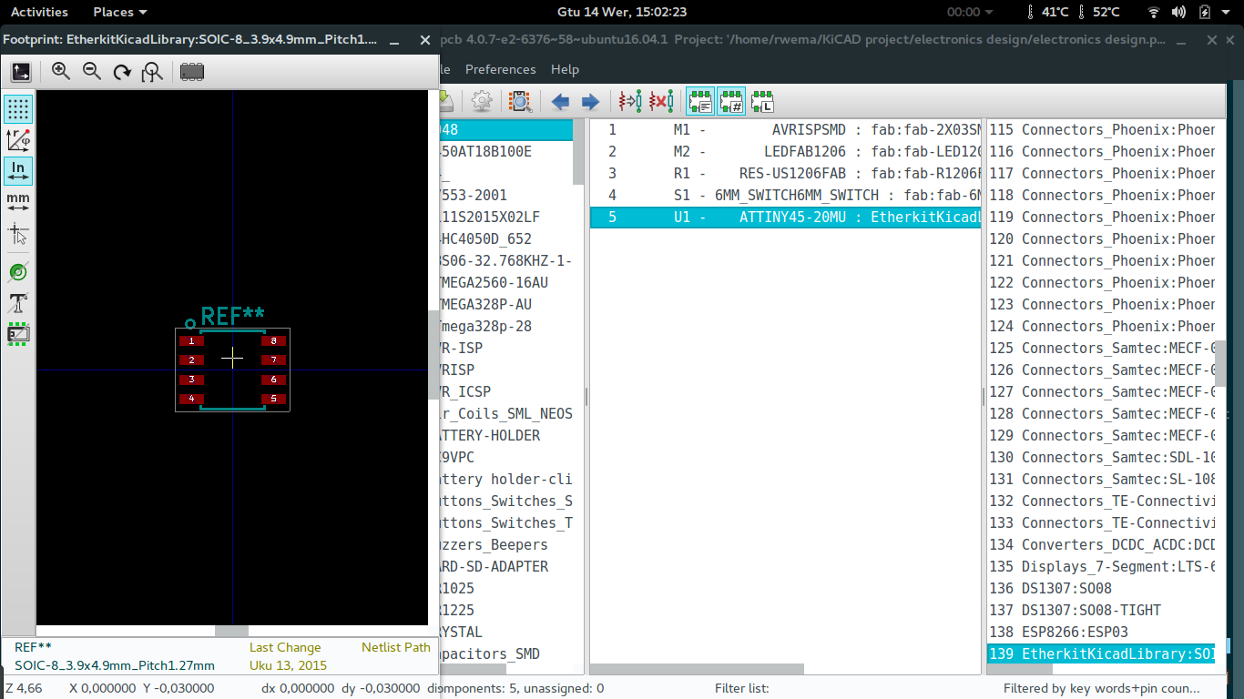
In KiCAD after designing the schematic you have to associate components to their footprints you will be using in designing the PCB.
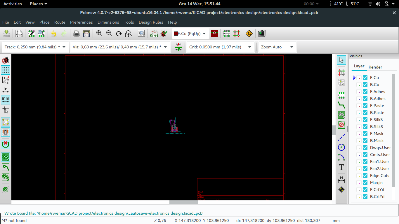
Now I am ready to start designing the PCB but first I have to generate the netlist which will take the connection I created in the schematic and transfer them in board designing.
In PCB designing, I first read the generated netlist to load the design I made.
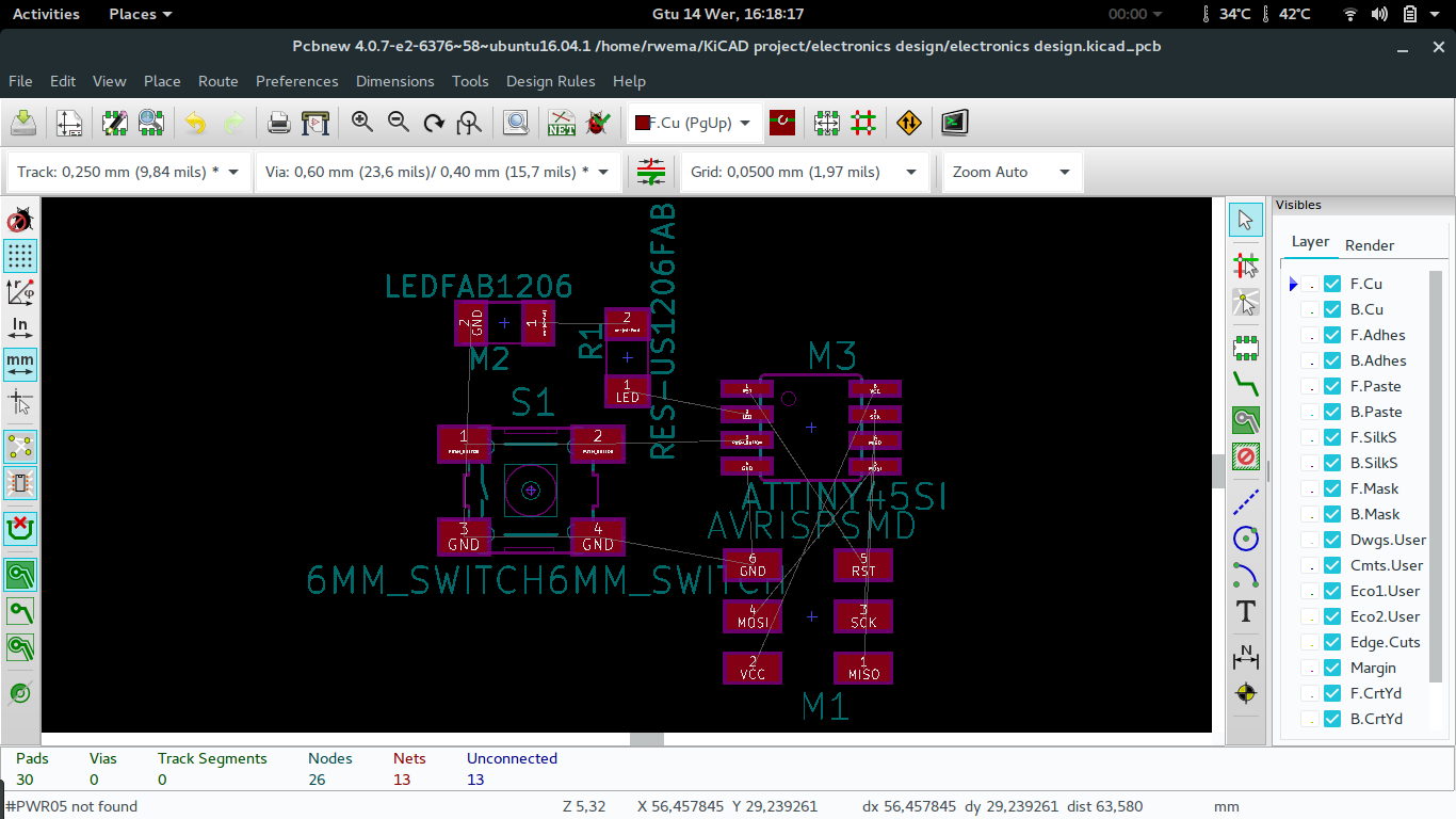
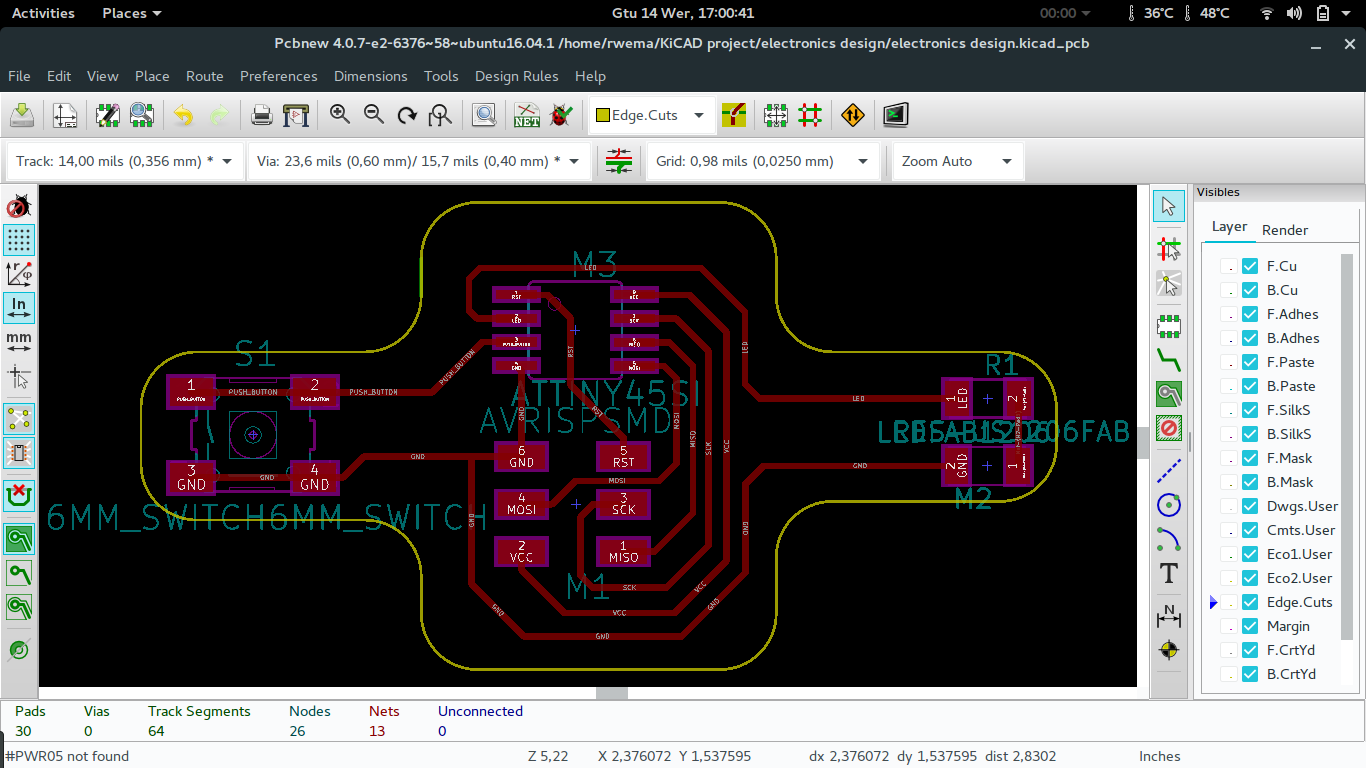
Now I started design the layout of the board. Every component has to be on the same side which is a bit complicated to implement without using jumpers.
For easy my routing I started on placing components which goes together aside, which saved me time.
After placing components as show above I noticed that I always use the same layout(square board) when designing, so I changed my mind and created a different layout randomly.
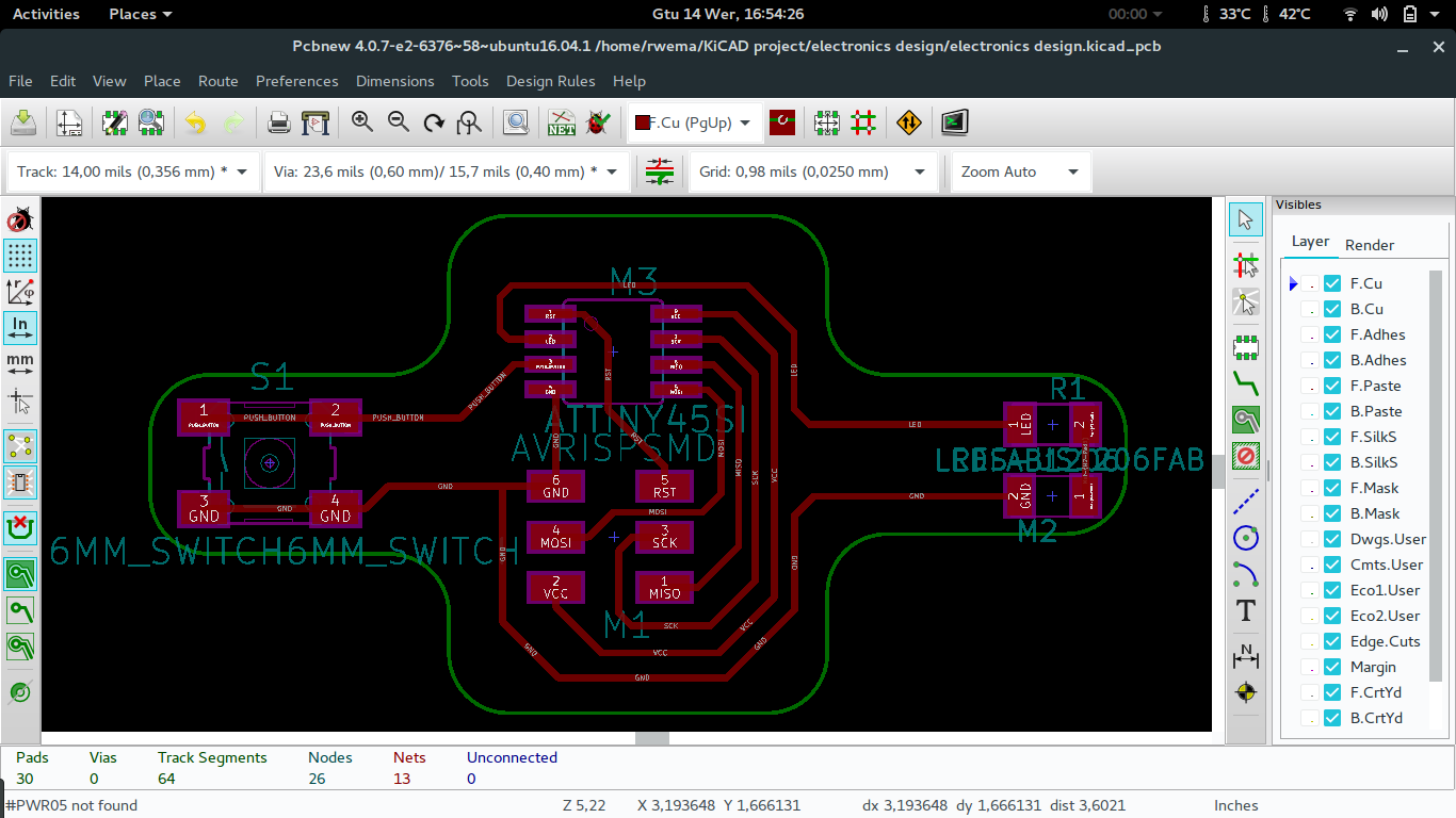
The following is the final design of the board.
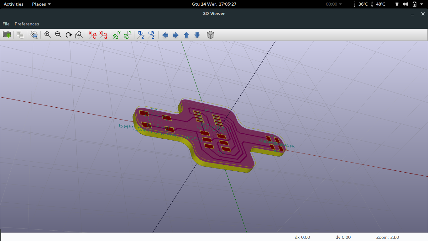
Something else I like on KiCAD is that it provide the 3D view of your board. This feature helps alot to see how the final result will look like before you start printing.
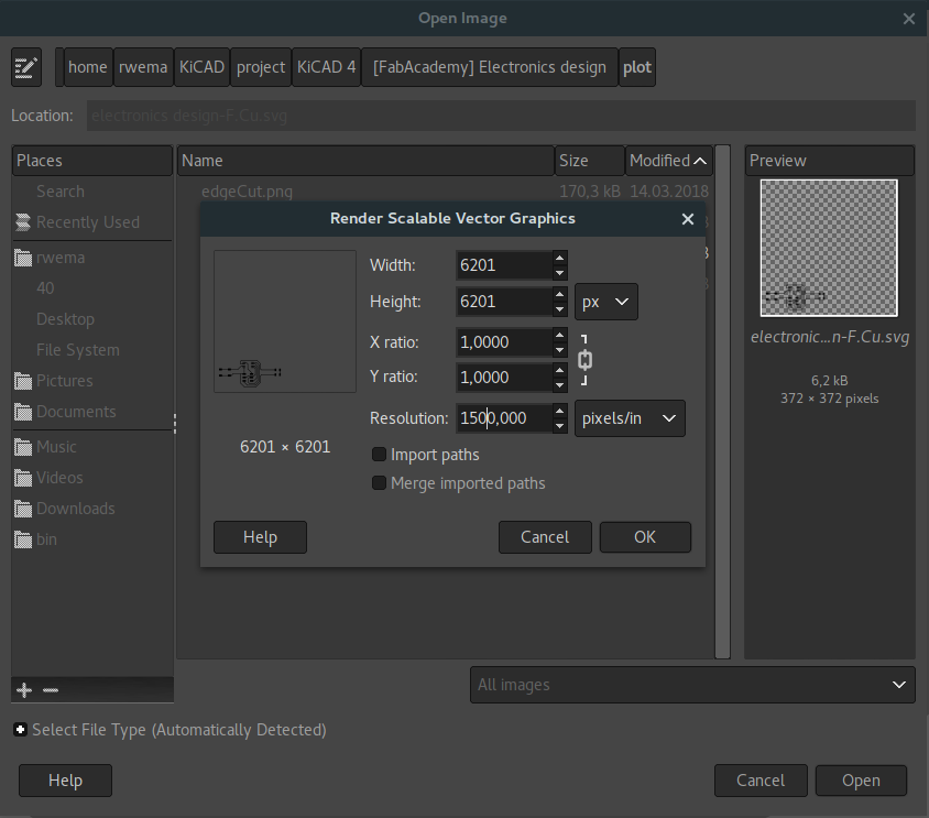
Now that I have created the PCB, I have to create files I to be used in fabmodules which will generate files roland machine can understand.
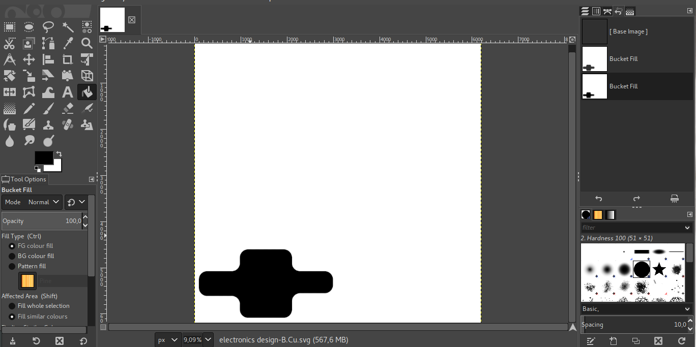
How I did create the file for fabmodules, I open plot feature of the KiCAD adn select SVG and plot only front copper F.Cu and bottom copper B.Cu. Below there are files generated.


Challenges faced while using KiCAD
For printing the PCB with monoFab I have to generate a PNG image of traces I used and convert them in RML files the monoFab can understand.
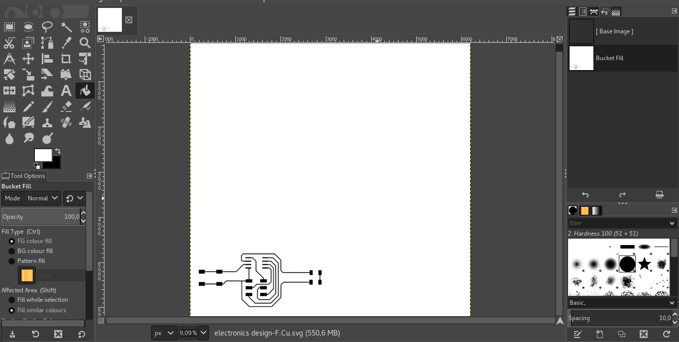
By default KiCAD can not generate PNG images but it can generate SVG file, so I generated SVG images from KiCAD and imported them in GIMP to increase their resolution and convert them in PNG. This is an extra work I have to do for all PCB I want to design compared to Eagle CADsoft which generates them directly.
Milling PCB
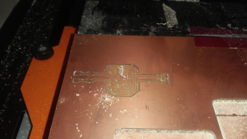
Now after designing the PCB I had to mill it.
After converting the generated png image to rml, I placed the PCB in the monofab and set origin point for starting milling. Traces milling was fine no issue I faced but when I started cutting the edge of the PCB the 1/32 drill bit break and I think it was old so I replaced it and everything went fine.
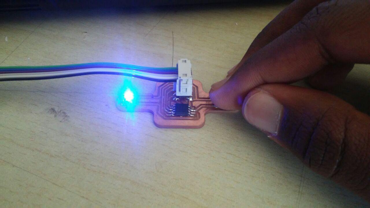
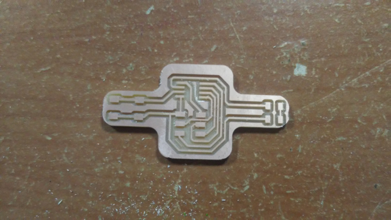
This is how the final result of the PCB looked like.
After printing the I soldered all the component in there place.
Component used:
| No | Component | pieces | Description |
|---|---|---|---|
| 1 | ATtiny45 | 1 | It is the processor and the circuit |
| 2 | Push button | 1 | This will be the input part of the circuit |
| 3 | LED | 1 | This will be the output part |
| 4 | Resistor | 1 | It is used to limit the voltage on the LED |
| 5 | AVR ISP | 1 | It is used to program the ATtiny chip |
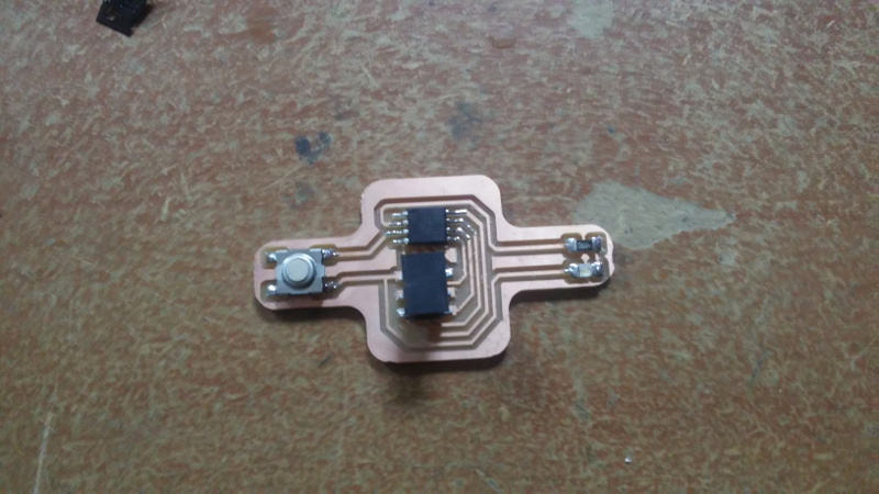
After soldering the board I programmed it.
The program I used and a video is on week 9.