Week five: Electronics production
This week is all about producing a functional PCB with components and all.
I started by opening Brian's tutorial in the fabacademy webpage, I downloaded the PCB files for the traces and board outline.
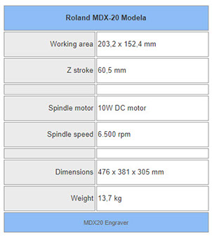
The machine we are working with is a Mini CNC Desktop Mill Modela Roland, you can click on the image of the specs to get the full PDF datasheet.
Process characterisation:
Here in Fablab Puebla we make a lot of prototype PCBs, we use them to test designs for projects, control machines or to teach students how they can build their own projects.
- For making this PCBs we first have to design the board. In this case the design was made by Brian (I couldn't find his last name) and I downloaded it form his page: http://fab.cba.mit.edu/classes/863.16/doc/projects/ftsmin/index.html
- Then we have to choose the material in wich we will enegrave and cut our PCB, there are a few materials out there like epoxy glass, pertinax, ceramics, teflon or a variety of polimers like bakelite. The chosen one here in the Fablab is epoxy glass because it is easy to machine and realtively cheap.
- The material can be placed in the sacrifice layer of the mill (wich is something you put over the work bed to avoid hurting it with the cutter, normally it is 3mm MDF) by three methods: by drilling holes on the material and screwing it to the sacrifice layer, by mounting it with clamps to the mill or the old favorite, double sided tape to the sacrifice layer.
- Soldering electric components to a board is done by heating to melting point an alloy (normally made of lead and tin that can have diferent combinations and also other metals depending on the specific use) and join the components to the copper surface of the board. As the range of temperature used in this process is below 400 degrees celsius, it is refered to as "soft soldering". The process of soldering is explained further below.
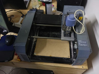
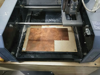
I first installed an MDF plate to the mill tray so the tool wouldn't get damaged. After, I taped the copper board with double sided tape and adjusted the Z height in the mill (you have to press the down button until the tool barely scrapes the surface of the copper board).
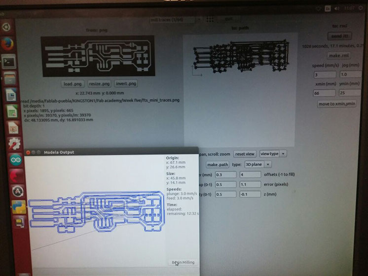
The parameters used for milling the traces were 0.3 mm for diameter, 0.5 for overlap, 0.5 for both top and bot intensity, 4 for offsets, 1.1 for error and -0.1 mm for Z. The diameter is the diameter of the tool, the overlap is the distance between one pass and another, the offset is the times the tool passes to make a trace.
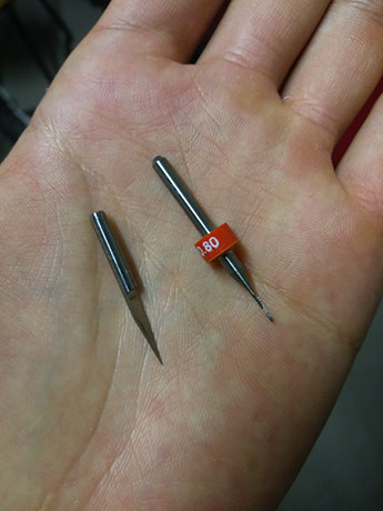
I opened Brian's file for the traces and set the parameters of the mill to: speed 3 mm/s and the diameter is 0.3 mm, I used an engraving tool (left) for tracing and a tungsten carbide cutting tool (right) for cutting the perimeter in wich I use 2 mm/s for speed and I change the diameter of the tool to 0.8 mm. Set the origin, click on make.path and then on make.rml, you'll get a path preview and the time remaining.
Click begin milling and pray that your double sided tape can hold on.
When finished change the tool for the cutting tool and repeat the steps for the board outline file.
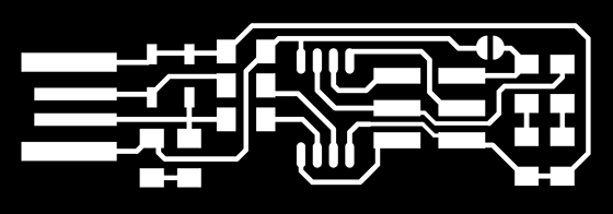
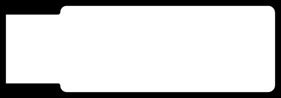
Clean the PCB to avoid shorts and sand it before soldering.
You have to be very careful when soldering, the hole soldering iron is 380 Celcius.
The process of solder is:
- Heat the copper and place the component over it (you can put a little bit of flux).
- Put a little bit of solder in the surface of the copper and quickly remove the soldering iron and the solder.
- Allign the component by heating the drop of solder and moving it with some
- Put the rest of the solder joints of the component.
Repeat and repeat and repeat with patience and determination.
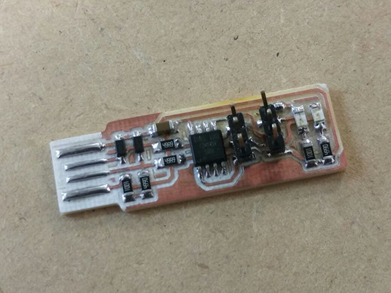
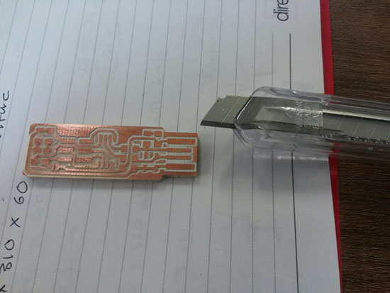
I used a little bit of flux paste as it was recomended by my guru, I first droped a little drop of solder in the surface of the board, then placed the component and melt the drop so a little part of the component would get attached, then I would solder the other side of the component and give the first part more solder.
For this board I used:
- X1 ATtiny45 (U1).
- X2 1kΩ resistors (R1 & R6).
- X2 49.9 resistors (R3 & R4).
- X2 499 resistors (R2 &R5).
- X2 LEDs (D3 &D4).
- X2 Zenner diodes (D1 &D2).
- X1 100nF capacitor (C1).
- X2 3Xpinheaders (MOSI, MISO, SCK, RST, VCC and GND).
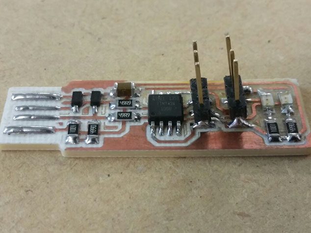
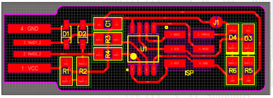
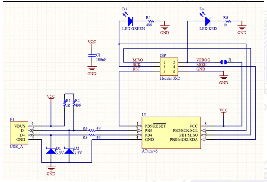
Programming the board
To program the board first I need a programmer, I'm going to use an arduino UNO for programming so first I upload the arduino ISP example to the board, then we can use it as our programmer.
I'll use avrdude in command prompt to run the program.
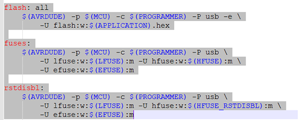
For programming the board I used Brian's Makefile which I found here: http://fab.cba.mit.edu/classes/863.16/doc/projects/ftsmin/index.html and oppened it in Notepad++, I eddited the lines showing on the right picture (flash, fuses and rstdisbl) by changing the the variables (color blue) to the original value, so they would end like this:
avrdude -p t45 -c stk500v1 -P\\.\COM20 -b 19200 -U flash:w:fts.hex
avrdude -p t45 -c stk500v1 -P\\.\COM20 -b 19200 -U lfuse:w:0xE1:m -U hfuse:w:0xDD:m -U efuse:w:0xFF:m
avrdude -p t45 -c stk500v1 -P\\.\COM20 -b 19200 -U lfuse:w:0xE1:m -U hfuse:w:0x5D:m -U efuse:w:0xFF:m
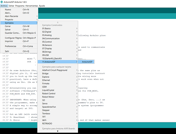
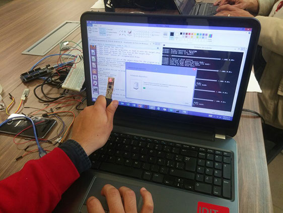
I ran each line at a time and it worked without problem but sadly I couldn't get a screenshot from it.
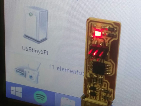
But here it is being recognized by the computer.
