Milling the PCB
This week we were assembling our own in circuit programmer that we will be using later on in the course.
The first thing we had to do, was to select what kind of Printed circuit board (PCB, in Finnish Piirilevy) we wanted to do. In this weeks FabAcademy site we were given some examples on how to carry it out using either ATtiny44 or ATtiny45 microcontrollers. I chose to use Brian's documentation, as it had a good introduction, and the advice seemed very simple and graphic, easy to carry out.
1. The first thing I did, was to download the traces file, and the outline file as image files (png) to my computer from Brian's documentation page. The traces file is basically the layout of your PCB, and the outline file will then be used to cut out your PCB.

2.The second step was going to the fabModules website and working on the files, to include your own milling machine specifications so that the board comes out right.
2.1 Here I have imported Brian's traces file, and selected the input format to be png. Now I am selecting the output format to be for Roland Mill (rml), which is the brand of milling machines that we have at FabLab Oulu.
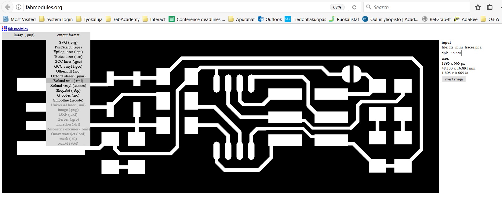
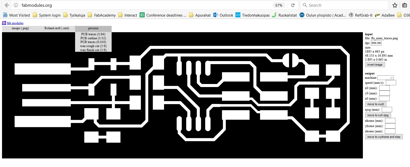
2.2 Next I specified the I am doing a PCB traces
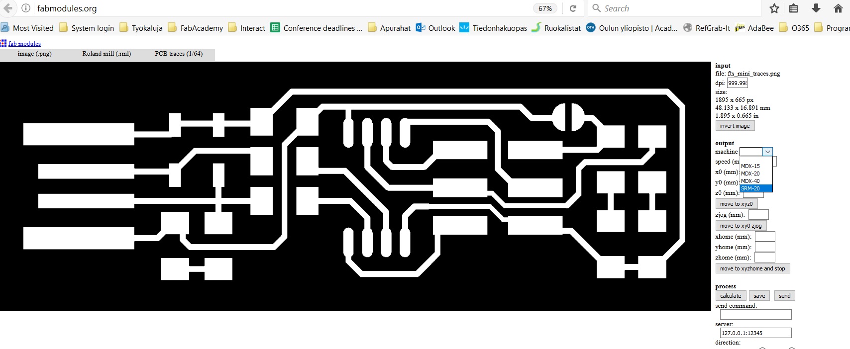
2.3 Then I selected what Roland Mill machine I am using - It is SRM-20. When I select this, the FabModules gives me some default settings for the machine. However, as different machines have different settings, mill heads etc. I then proceeded to modify those settings according to what our local instructor advised us.
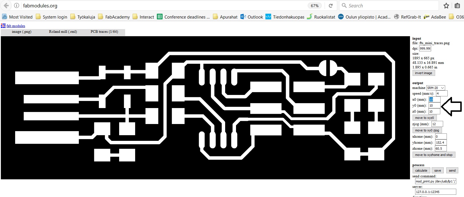
2.4 I changed the x,y and z values from 10mm to 0mm.
2.5 I let the process settings be as they are, but understood that cut depth and tool diameter settings here are the most important one. If the milling is shallow (some copper traces are left behind), these are what you would change. In FabLab Oulu we are using V-shaped milling heads to to do traces, and the settings with our Roland Mill SRM-20 are cut depth 0.1mm and tool diameter 0.4mm. I proceeded to press calculate.
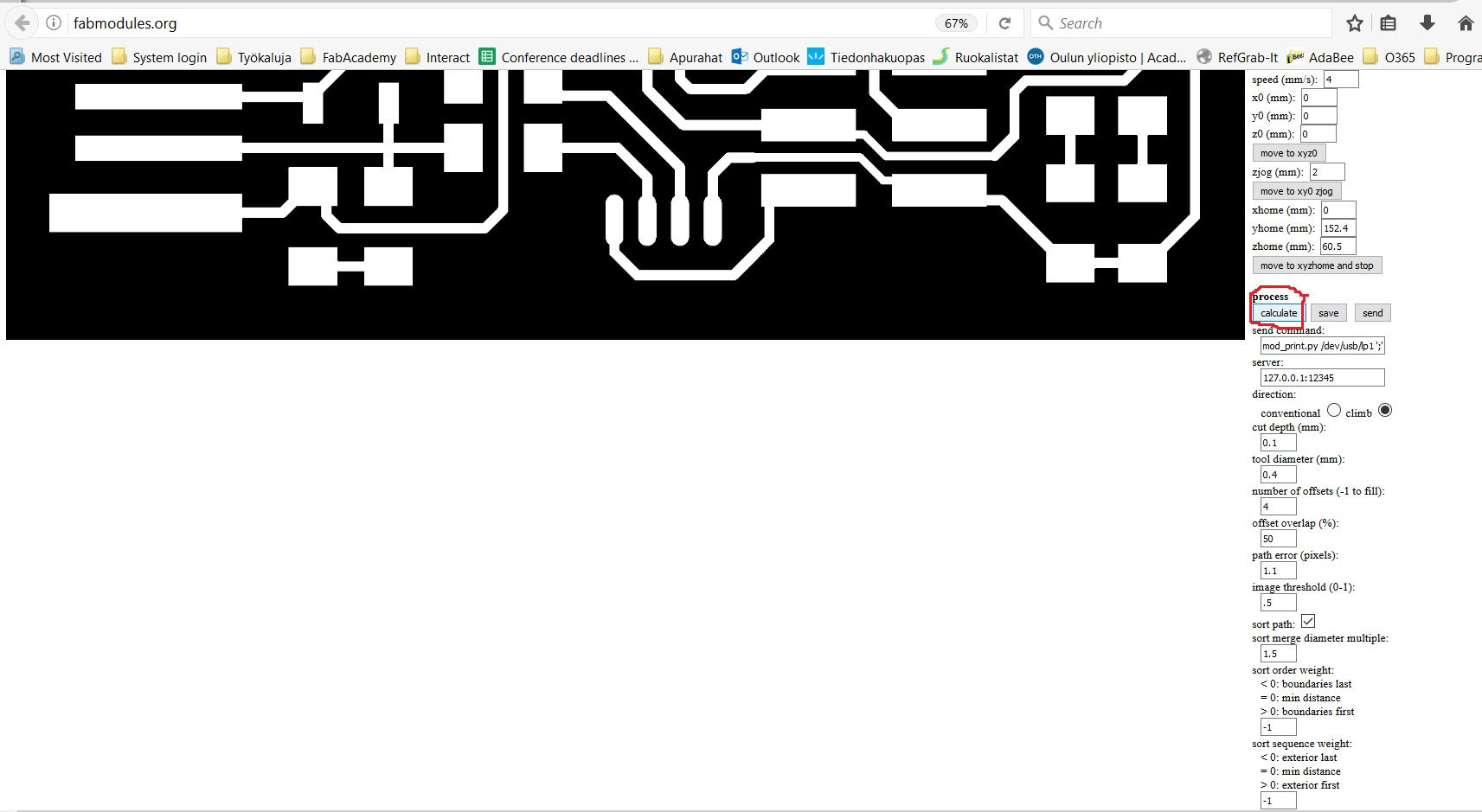
2.6 Pressing calculate then shows me milling lines and offsets.
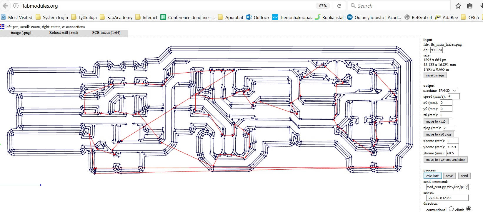
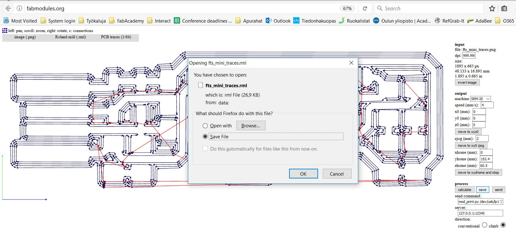
2.7 Now my file is ready, and I pressed save to save the rml file onto my computer.
2.8 Next it was time to start working on the outline file. I again defined that the input file is image (png), and that the output format will be Roland mill (rml). Next, I specified that this time i am doinf PCB outline.
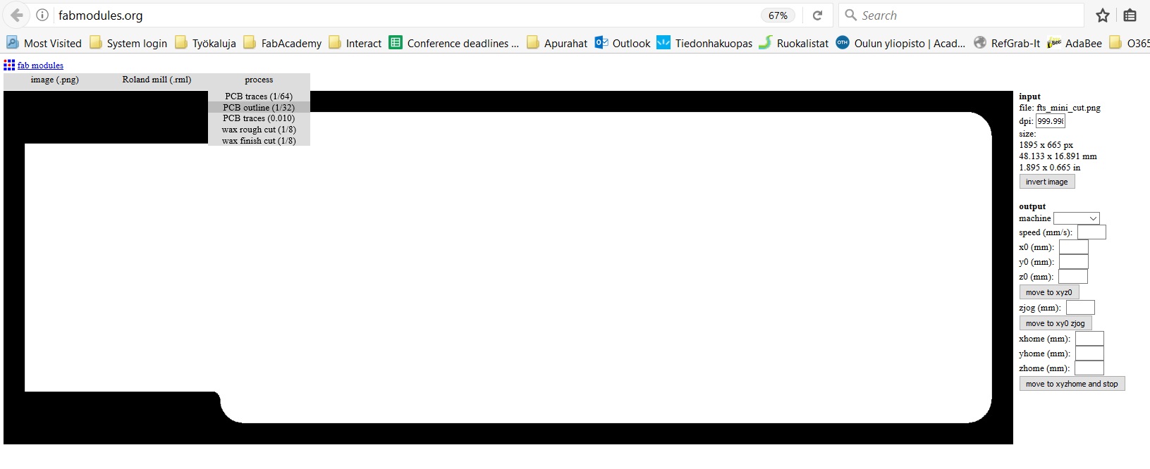
2.9 I selected the output machine to be the SRM-20 again, and changed x,y and z values from 10mm to 0mm.
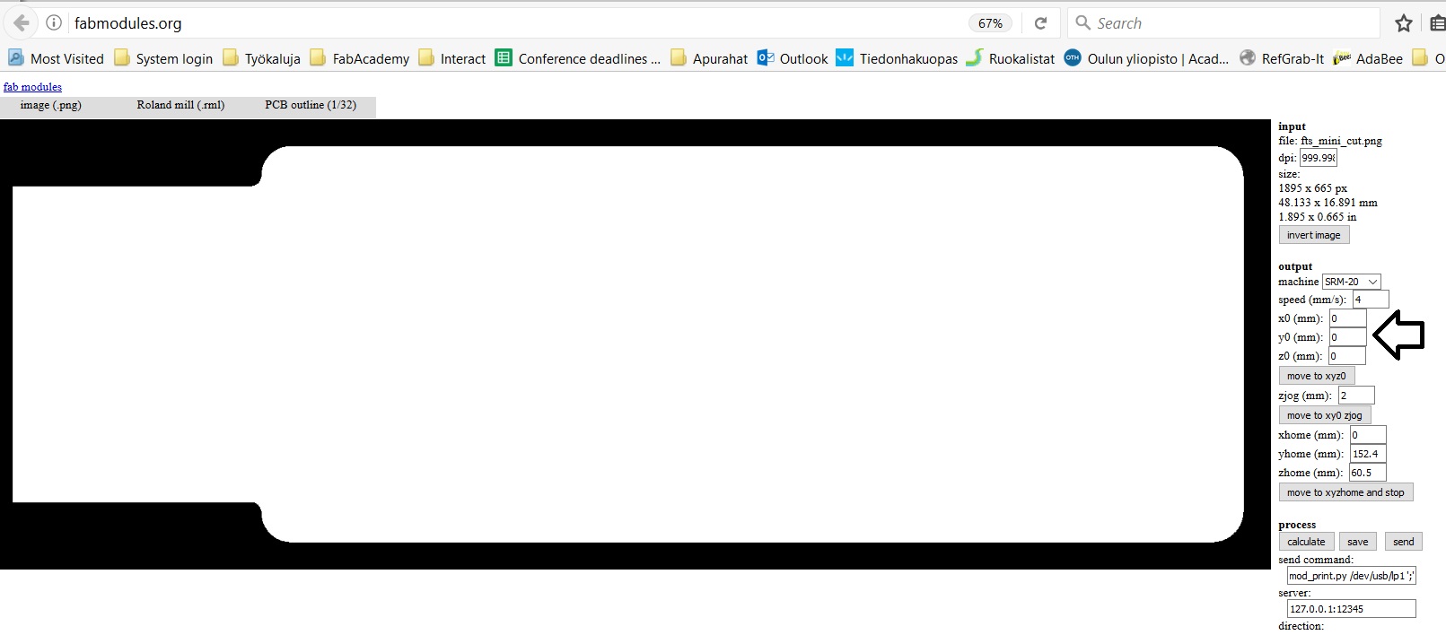
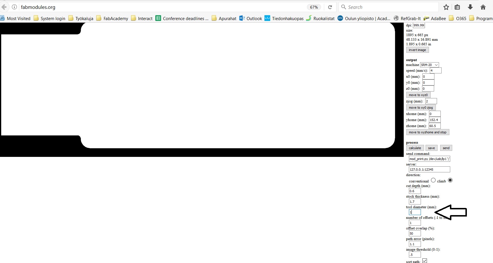
2.10 This time, we also changed the tool diameter. It was changed from 0.79mm to 1mm. In FabLab Oulu the settings with our Roland Mill SRM-20 are cut depth 0.6mm and tool diameter 1mm.
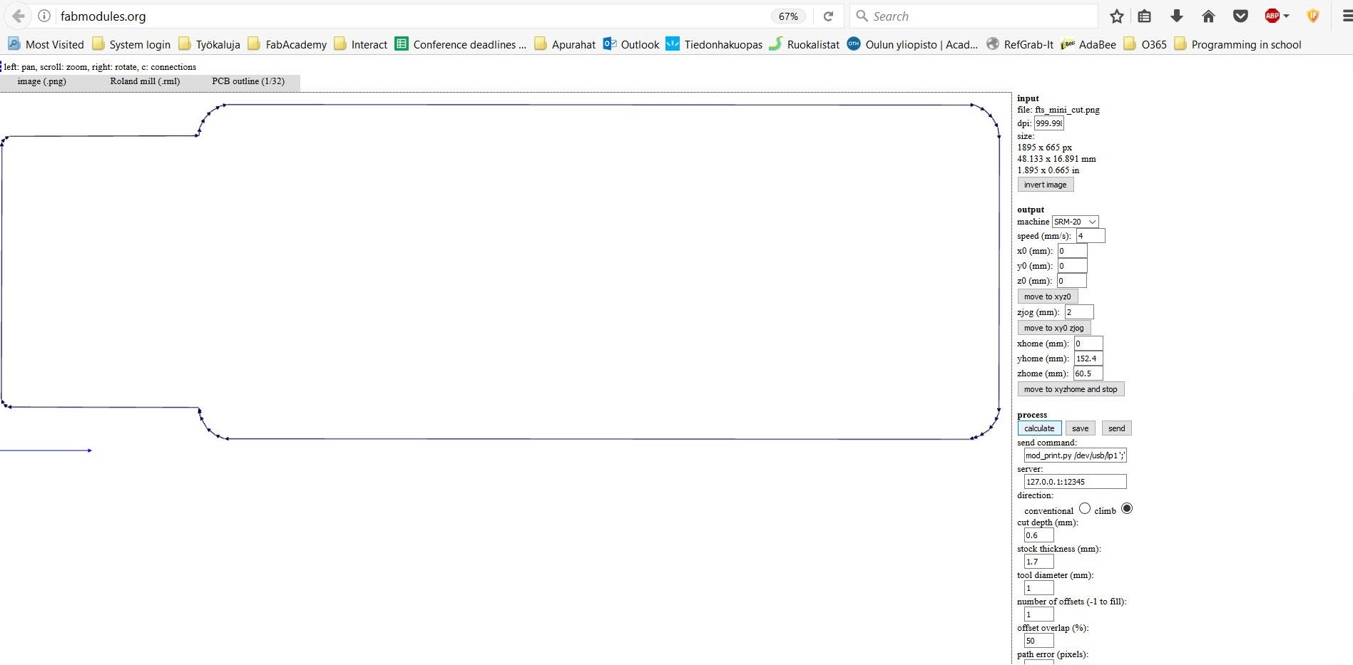
2.11 Pressing calculate again gives me a picture that shows me milling lines and offsets.
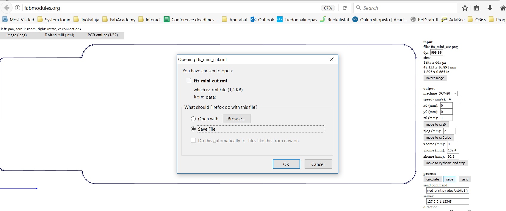
2.12 That picture is then saved to the computer as a rml file.
Files
- fts_mini_traces .rml file
- fts mini cut .rml file
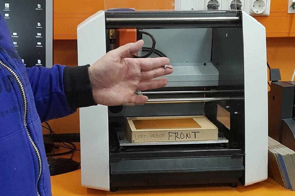
3. The third step is taking your rml trace and outline files that include the milling lines and offsets, and heading towards the milling machine and the computer that it is controlled with. Here is the Roland Mill SRM-20 that is used in FabLab Oulu.
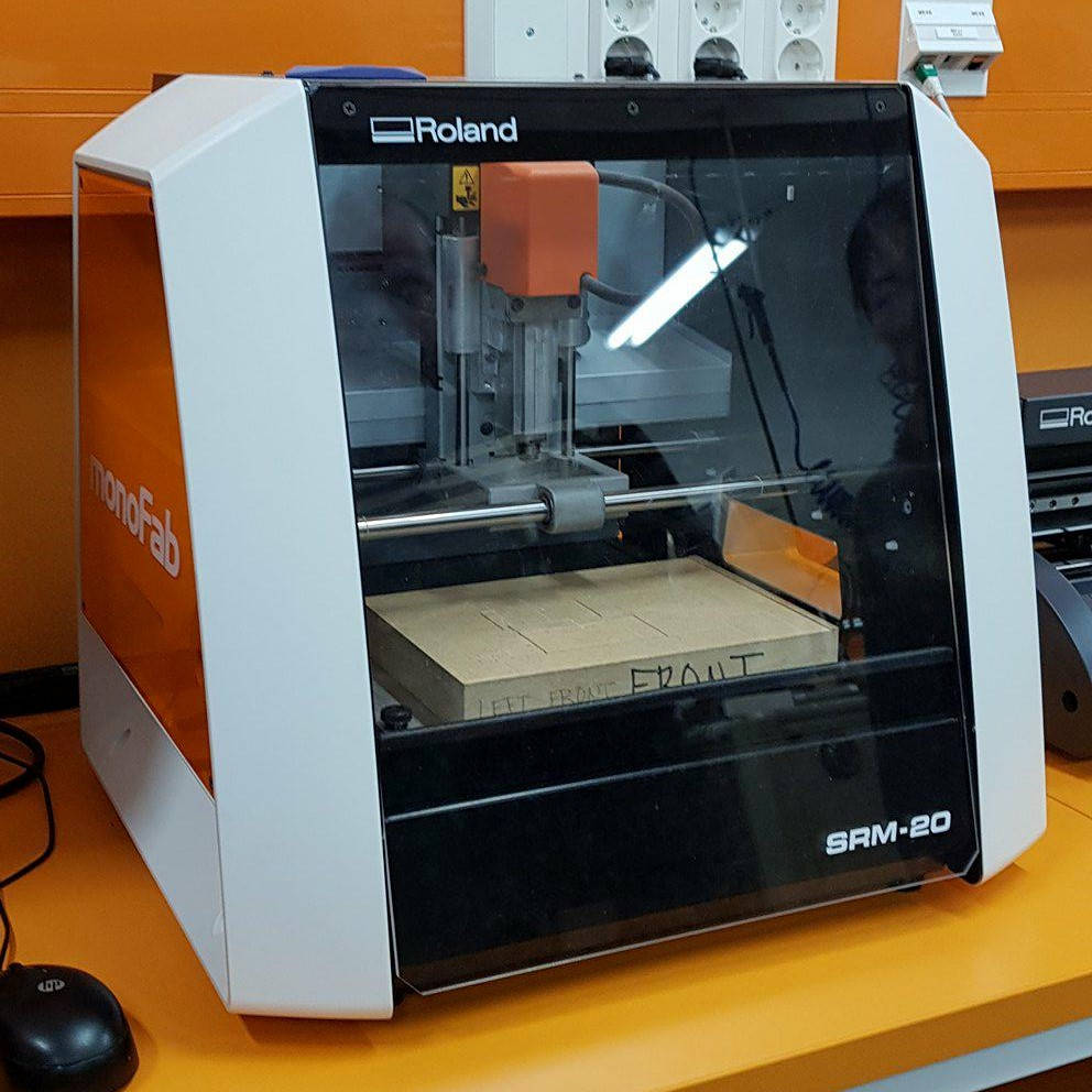
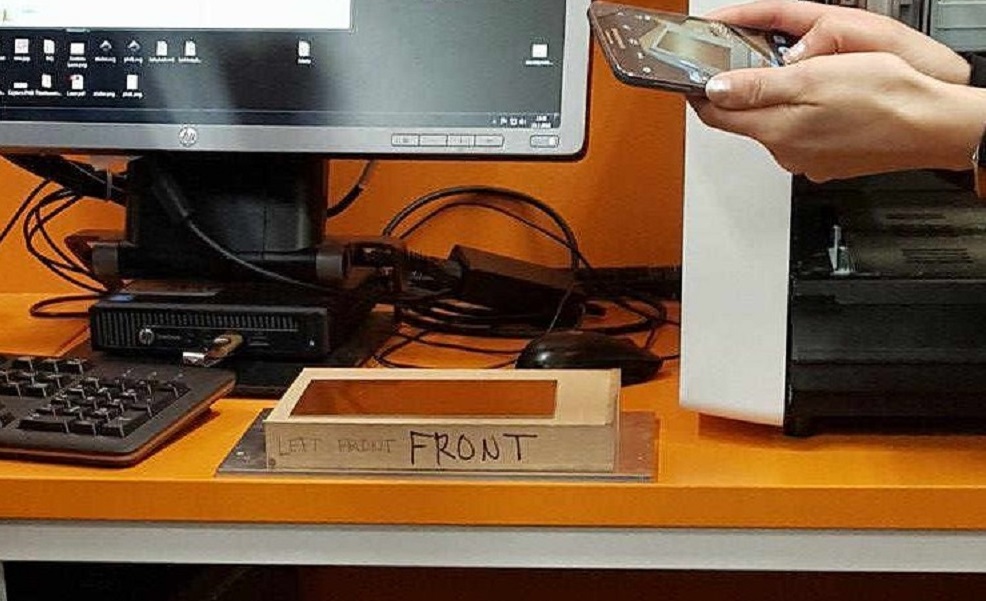
3.1 When working with the machine, the first thing to do is to insert the copper plate that you will be milling your PCB into. First, you remove the inner baseplate that is used to secure it.
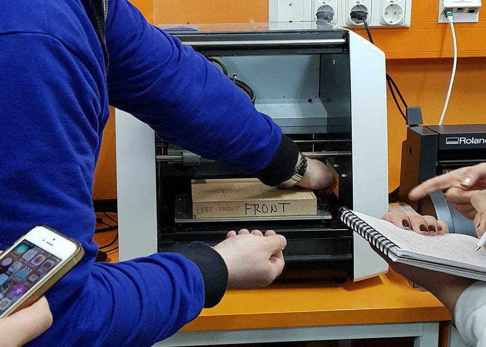
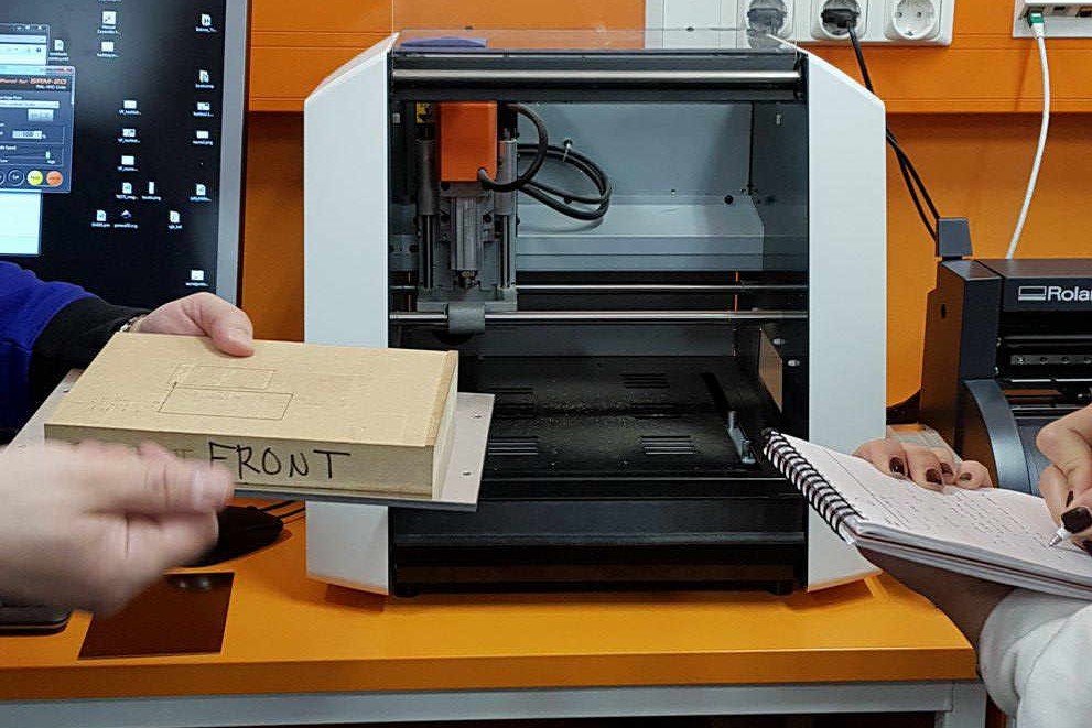
3.2 Then you take out a fresh copper plate, and put double sided tape on the bottom, so you can secure it to the base plate.
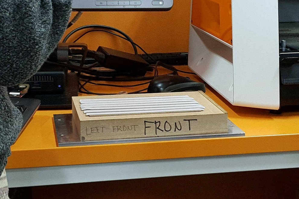
3.3 You secure the copper plate with the tape, and remove the protective film from the top of it before putting it back to the milling machine.
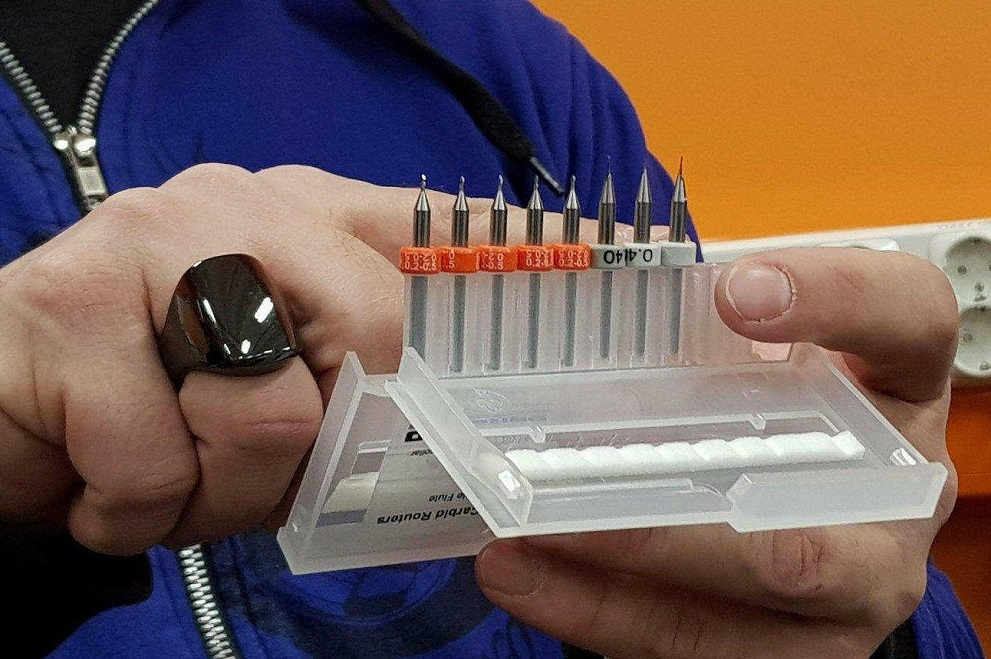
3.4 Next you change the milling head into the milling machine. Pictured here are the milling heads we use at fablab Oulu, the orange ones are V-shaped, and you can cut anywhere between 0.2mm and 0.5mm width with them, depending on the tool depth. The grey ones are an alternative for the orange heads, their size is 0.4mm.
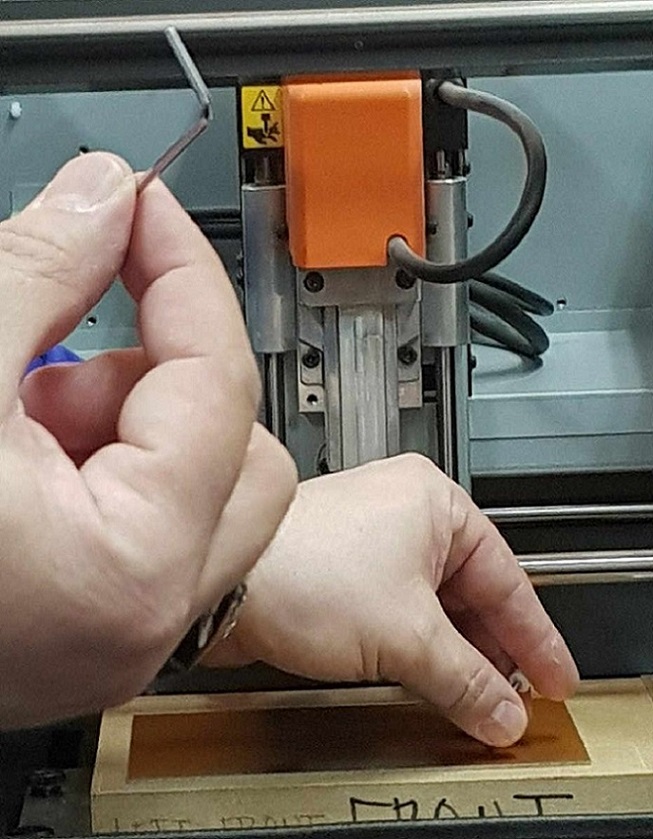
3.5 To change the milling head, you first loose the allen key to loosen up the first milling head, put it away securely, and then use the allen key again to secure the new milling head to place. You have to be careful here, as the tips of the milling heads are very fragile - Do not drop them or press them against anything.
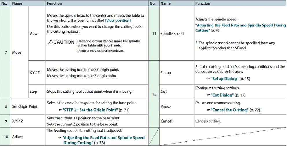
3.6 Once you have the copper plate and the baseplate, as well as the correct milling head secured in the milling machine, it is time to open up the application that you use to control the machine. the UI of the Roland Mill at FabLab Oulu is called VPanel for SRM-20. The basic functionalities are displayed in the pictures below, acquired from the SRM-20 user manual.
When you have the user coordinate system selected, you can freely select the location of the origin point for the milling.
- Use the XY movement keys (5) to move the milling head to the front left corner of the copper plate (or the place where you want to start your PCB), and then hit the X/Y button (9) to set the origin.
- Use the Z movement keys (5) to lower the milling head close to the copper plate, then used the allen key, loosen the milling head so that it touches the copper plate, and then tighten it back on (This is so that you do not break the head if you automatically lower it too much). then hit the Z button (9) to set the Z position of to the base point (9), and used the Z movement keys to lift it a bit from the plate.


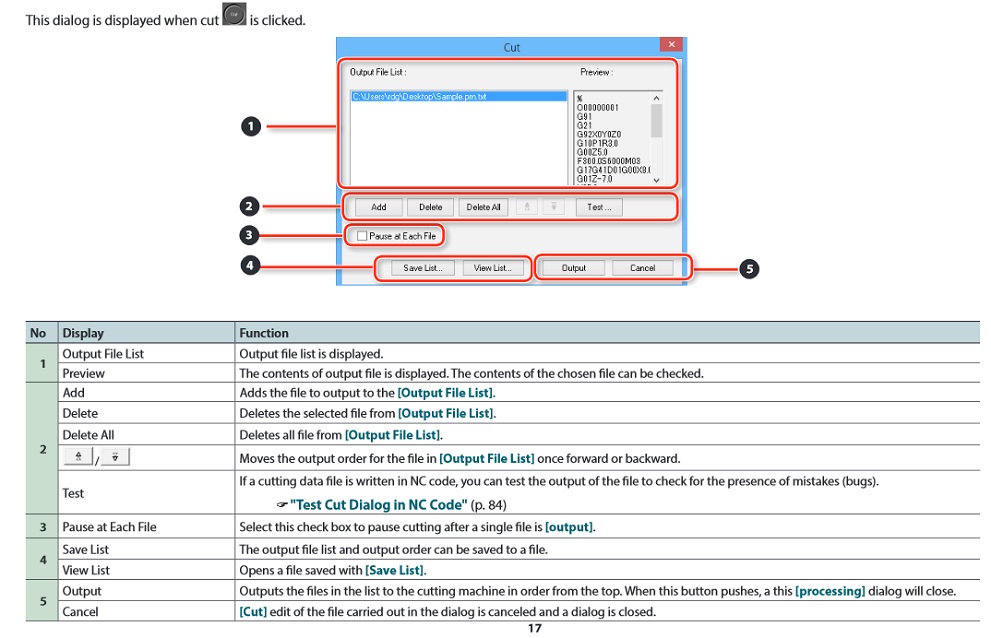
3.7 Next press cut, and this dialoque window opened up (photos from the SRM-20 user manual Clear the cutting queue by pressing "delete all", and uploaded your own traces file there. Next press the output button (5) to send your file to the machine to be milled.
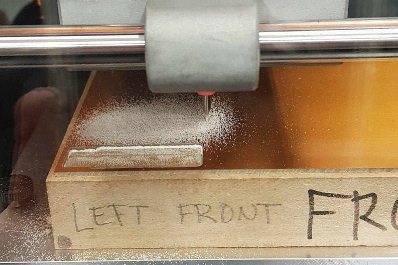
This is my PCB traces being milled
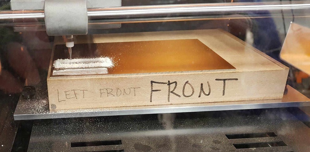
3.9 When the traces are milled, you vacuum the board (without removing it from the machine). After that you then have to cut the BCP out of the copper board. First you change the proper milling head to the machine. We used the 1.0 mm tool. Then you repeat the some of the steps described above for the outline file:
- Press Move to X/Y, but do not change XY coordinates anymore
- Use the Z movement tool (5) to lower the milling head close to the copper plate, then used the allen key, loosen the milling head so that it touches the copper plate, and then tighten it back on. Then hit the Z button (9) to set the Z position of to the base point (9), and used the Z movement keys to lift it a bit from the plate.
- Next press cut, and a dialoque window opened up. Clear the cutting queue by pressing "delete all", and uploaded your own outline file there. Next press the output button (5) to send your file to the machine to be milled.
This is my PCB outline being milled
3.10 Once the outline has been cut, vacuum the board again, then carefully remove your PCB from the machine. (If there is usable copper board still left, leave it there). After removing the PCB from the machine, rub it with steel wool.
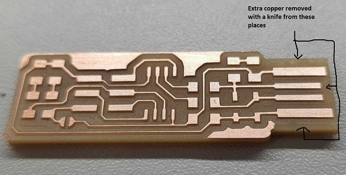
I had to remove some extra copper from my PCB when it was ready, before going on to assemble the board
Assembling the PCB
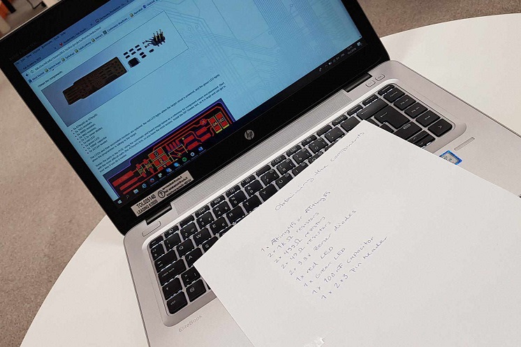
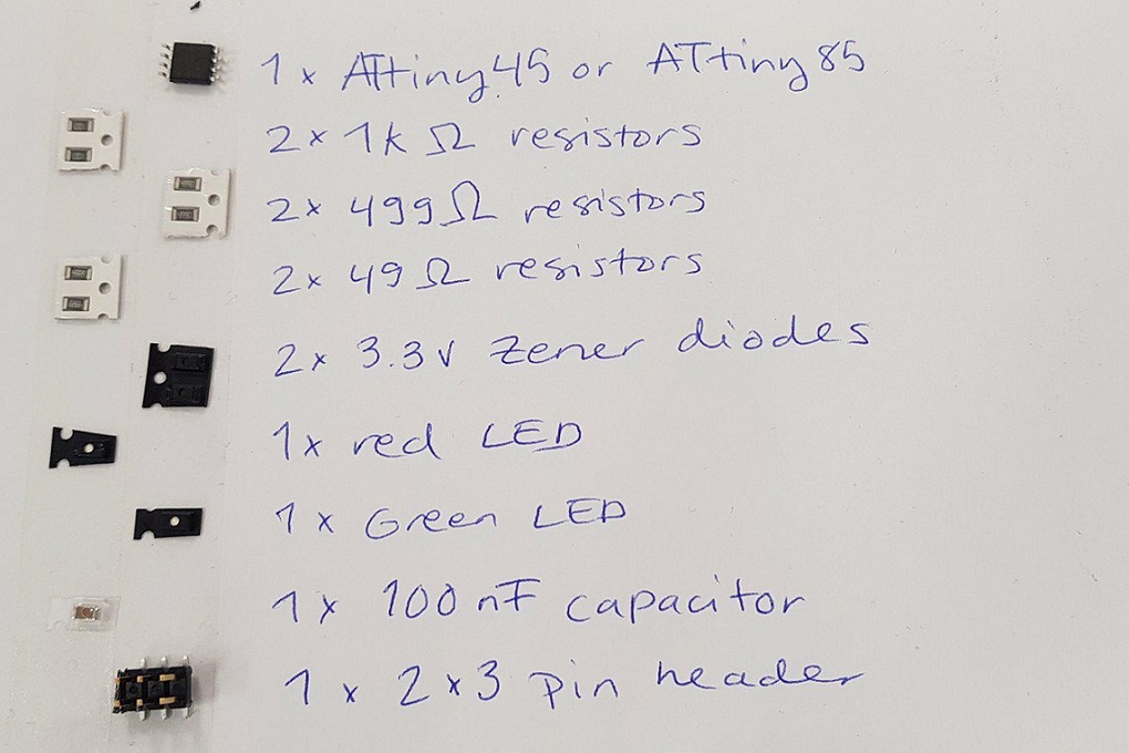
I found the component list for the board also in Brian's documentation, copied it to a sheet of paper and went into our supply room for a treasure hunt.
I secured each component to the sheet of paper using double sided tape. I think this is a good idea for newbies, as I could not tell the parts apart otherwise. All the parts are also very light, so this way they stay organized
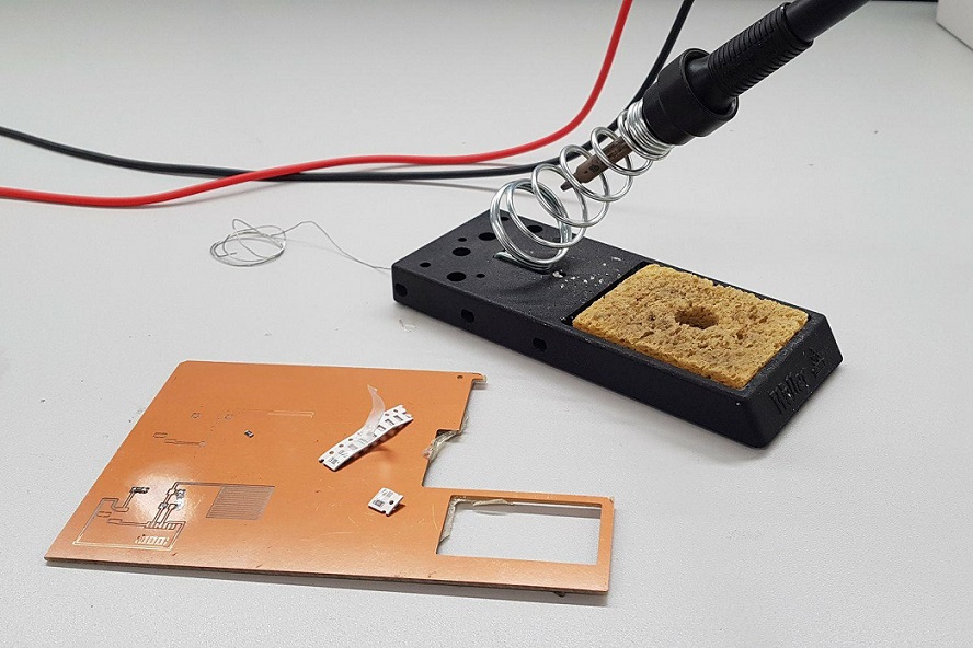
I turned the soldering iron on and wettened the sponge where you clean the iron. I also turned on a device that sucks any fumes that occur when soldering. Then I also got me some tin for soldering and a few spare components, and before starting to work on my own board, I did some test runs on scrapped boards that were due to be destroyed. Just to get a feel of how it goes without doing any damage to my own board.
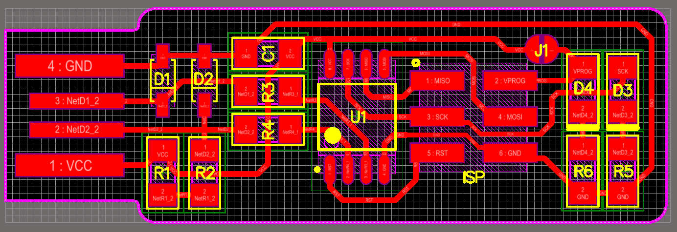
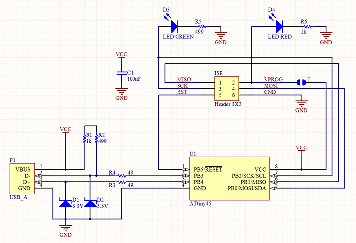
When starting to solder, I kept my computer next to me, and looked for help from the board layout and schema pictures from brian's documentation on how to assemble it
Brian's board layout
Brian's schematic
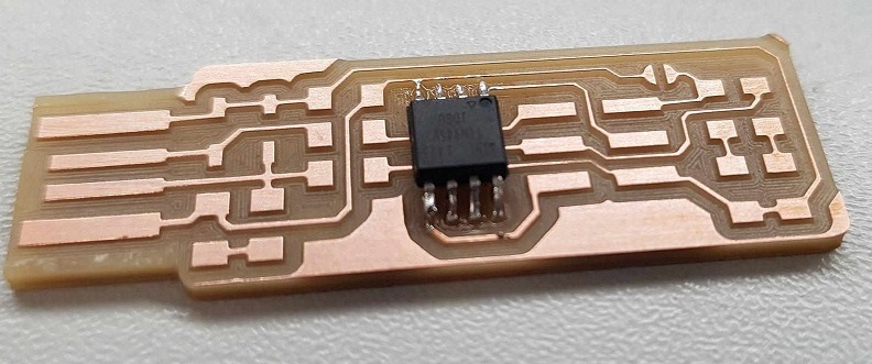
The first thing I soldered to my own board was the ATTiny. Little did I know at this point that I soldered this on the wrong way. I did not notice the huge yellow dot on the board schema that corresponds to a dot in the component that needed to be matched...
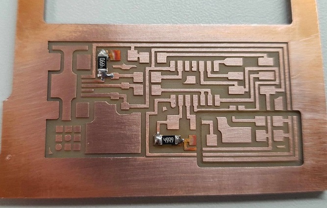
Blissfully unaware of my mistake, I continued to solder on the resistors needed.
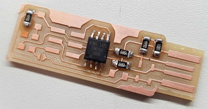
Then our local instructor Jari came and saw what I had done. Thankfully the ATTiny could still be removed with the help of a desoldering braid.I placed the braid on over the legs/pads I wanted to be desoldered and placed the iron on top of the braid --> This way the tin got absorbed into the braid.
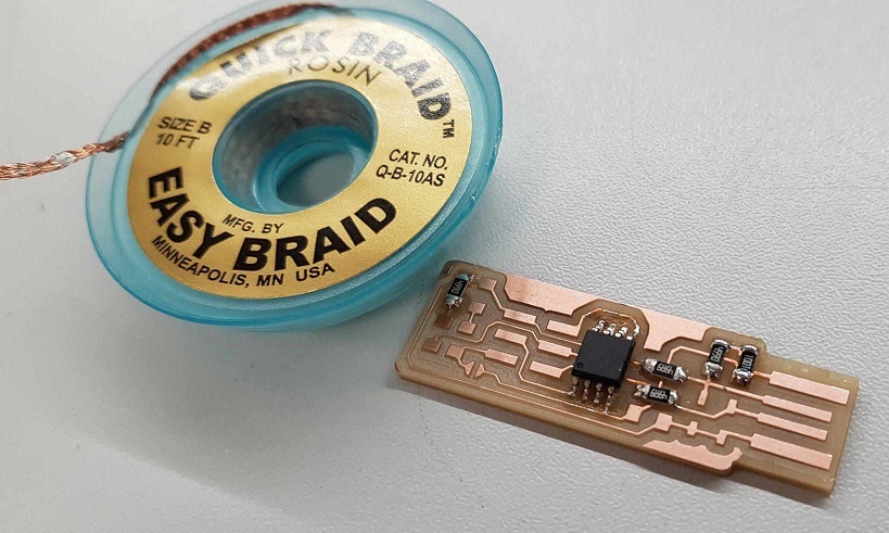
Just to be on the safe side, we however replaced the ATTiny component, in case I did some damage to it having to solder and desolder it again.
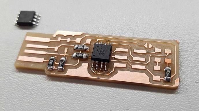
I progressed through soldering in the last resistor, and the 2 zener diodes. Next I soldered in the red led. Leds were also components that need to be soldered in a certain way, the green stripe on the top of the component indicates that that side needs to connect to ground.
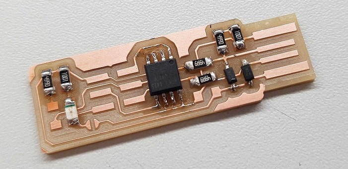
Here I also soldered in the last components, the 3*2 pin header, and the green led. As I could not for the life of me create/solder a bridge on the jumper, I used a 0 resisor here. It was explained in the documentation that this bridge is needed to temporarily connect "VCC to the Vprog pin on the ISP header so that the header can be used to program the tiny45. (The programmee supplies voltage on this pin and the programmer detects it)." So I gathered that means that the bridge is needed to program the board.
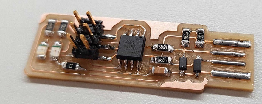
Programming the ATtiny45
We programmed our boards together after the soldering was finished. We had one computer with the necessary firmware installed and a programmer from previous year that we connected to it.
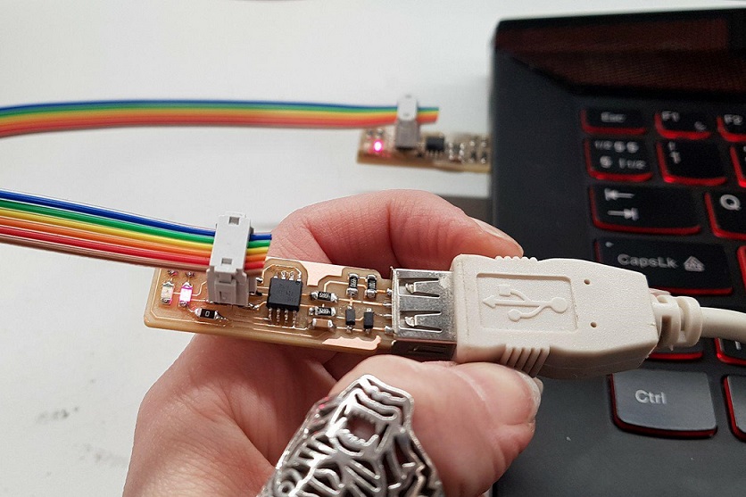
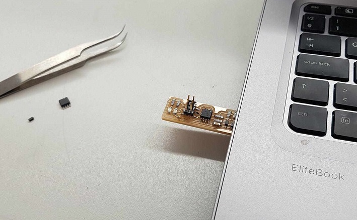
First I connected my own board (pictured in the foreground) to the computer using a usb extension cable. The red led lighted up. Next I connected my board to the already existing programmer that is attached to the computer from the 3*2 pin header.
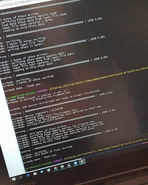
We ran the make flash command in GIT bash
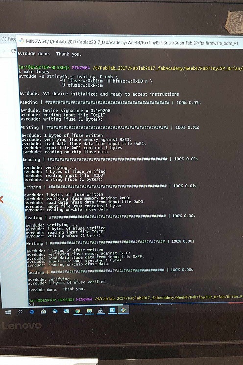
And the make fuses command
Once the board was programmed, the bridge (or in my case the 0 resistor) was removed, which turns the board into a programmer rather than the programmee. *
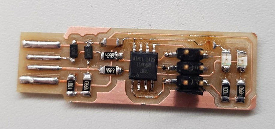
Then I attached my board to my own computer to see if it is recognized as a USB device
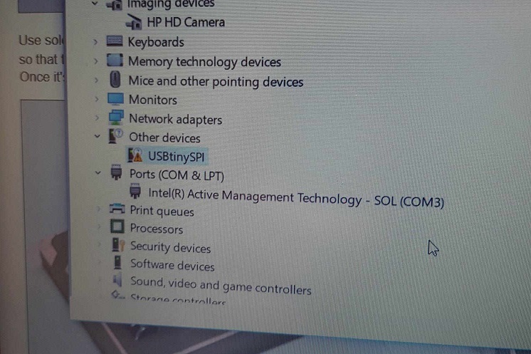
It was! Here it is visible in the device manager, great success!
*Note: Apparently, we forgot to do one command specified in the instructions - make rstdisbl (reset disable). This should have been done after checking that the USB on our board works, and before removing the bridge/0resisor. This command would have made it so that this this ATtiny45 could not have been reprogrammed in the future. So we were too hasty. As I understood it, this is however not a problem, just as long as we only use this board as a programmer
Even though we programmed our boards using one computer where the necessary development environment was already installed, I later on also installed it into my own computer using Brian's instructions which are very detailed and easy to follow. --> This is because we will need to be able to use our own boards to program other boards later on in Fabacademy.
What I installed was:
- Atmel GNU Toolchain
- GNU Make
- avrdude
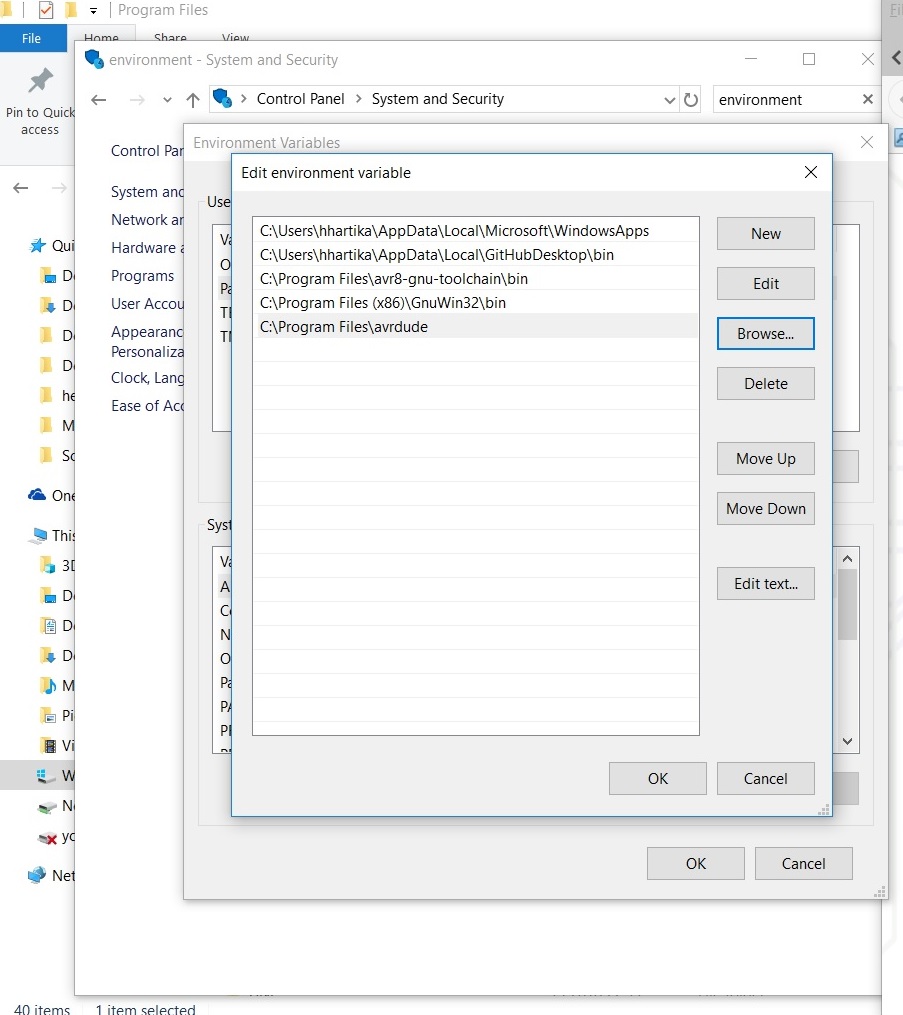
Next I updated the "path" under environment variables to tell Windows where to locate all of the tools I installed. Environment variables are located in the control panel of your computer. Open them up, choose path --> edit, select new tool to add a new line, and then browse in to the folder where you have the tool. Click OK.
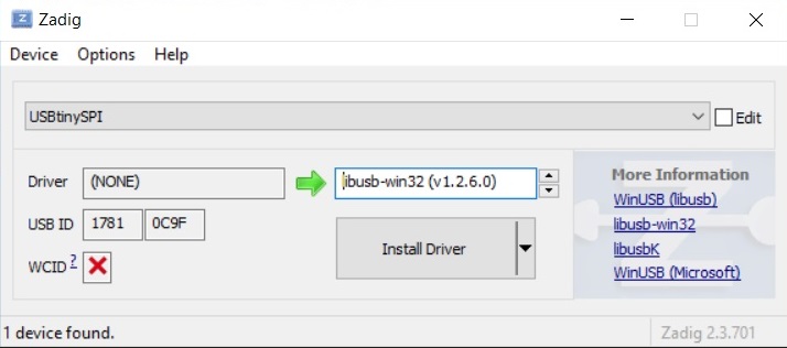
Next there was a need to install drivers for the FabISP, to do this, I downloaded Zadig and installed it the correct drivers
And lastly I did the sanity check to see that all works
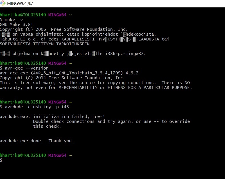
Note: Even though all seemed to go well this week, sanity checks and all, when I actually had to start using this programmer on week 7, it did not work.
We did the following, together with our local instructor Antti:
- He used his own programmer to program the board I had tried to program just to double check that the problem was with my FabISP. It worked just fine so we were able to isolate the problem to my FabISP
- He checked if either my programmer or the board I tried to program had short circuited. This did not seem to be the case
- He checked the soldering of my board, which seemed to be in order. Just in case he strenghtened the earth connections in some places with more tin.
--> Lastly I soldered the jumper back on, reprogrammed my programmer using Antti's board following the instructions above. After this it worked and I was able to use it on my hello world board.
Problems had, lessons learned, questions that remain
- If you haven't soldered before, it is probably a good idea to do some testruns beforehand on the smaller components like resistors. Apparently they do not cost that much, so it is no big deal if you ruin a few.
- Always, always check if some components need to be soldered on a certain way. I didn't.
Copyright © Heidi Hartikainen 2018
Template copyright ©Blackrock Digital LLC 2013-2018

This work is licensed under a Creative Commons Attribution-NonCommercial-ShareAlike 4.0 International License.