Week 5: Electronics Production
This week's tasks:
- Group assignment:
- Characterizing the specifications of our PCB production process
- Link to the Group Assignment Page
- Individual assignment:
- Making an in-circuit programmer by milling the PCB,
- Then optionally trying other processes.
Challenges that I faced while milling the PCB:
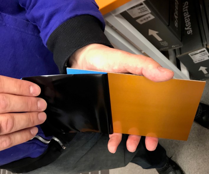
- After a few students used the same blank PCB and milled their pieces and removed their pieces, I started to use the remaining free space of the same blank PCB. But it did not cut it deep enough. Although we were all using the same machine and settings, it didn't work for some people. And we came to the conclusion that after a few times that students remove their pieces from the blank PCB, the height of the surface goes under some changes and affects the rest of the surface. So in this case, one solution was setting the origin of z, 0.1 mm under the surface, which means cutting depth now is (0.14 mm + 0.1 mm). Another solution could be that when a student mill something just wait for others to mill their pieces and at the end when all the blank PCB is used, people start to removing their pieces. In this way, everyone could cut with the same setting and do not need to bother with figuring out the new cutting depth for any specific situation.
- Assembling the PCB was quiet challenging initially. Since the components were really tiny and I was kinda scared to touch them :-D But after assembling 2,3 of them, it was kinda enjoyable feeling to work with those tiny things. I mostly had some difficulties at those moments that I used to solder one leg of a component at one side and then I realized that the other leg would not fit on the trace. So I had to remove it and redo it :-D Special thanks to Jari for paving this almost difficult way for me and I assume for some other students with zero experience in electronics production, by patiently instructing us.
Considerations:
- When you want to download PNG files, it is better to right click on the name of the image link and then save link as image. Because it happened to me that I opened the image in a new page and then saved it from there and the scale of the image got changed.
- The size settings for our design should be always bigger than the tool diameter, otherwise the tool cannot fit in and affect the result.
- ALways if you get a bad result, check if mill is OK.
Changing the Setting for PNG Files for the Traces
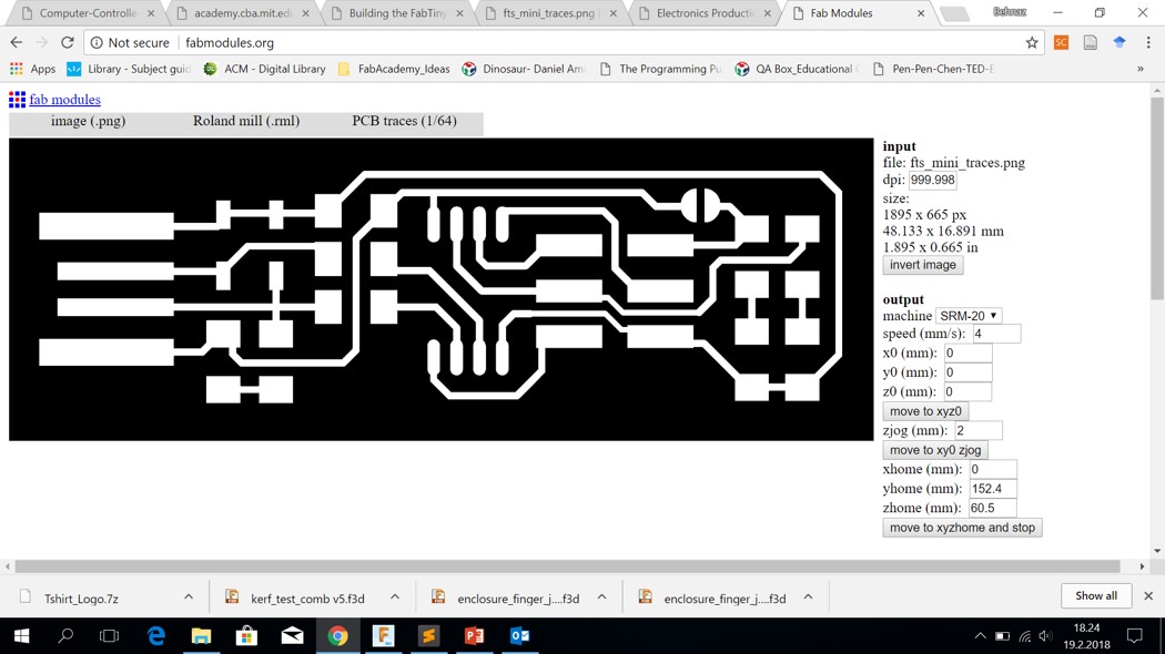
- Download the PNG files for the traces. I downloaded the image of traces and outline from Brian's page.
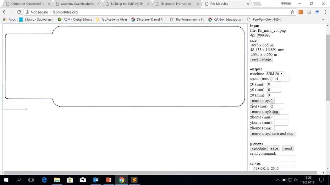
- Open fabmodules.org
- Input format: image (.png)
- Output format: Ronald mill (.rml)
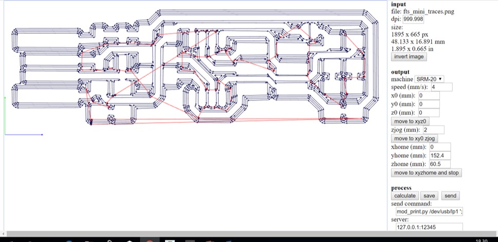
the output settings:
Machine: SRM20 - Process: PCB traces (1/64)
The settings for Process:
cut depth: 0.14 mm (cut depth: How deep the mill goes while it is cutting.)
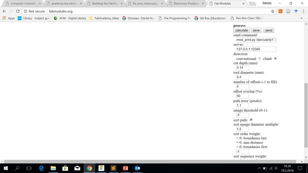
- Press 'calculate' under the Process
- Hit save button under the process to save the result.

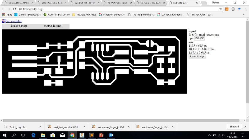
Speed: 4 mm/s
x0, y0, z0: 0 mm
tool diameter: 0.4 mm
The screen bellow looks empty but it is not empty. I scrolled down and the image is in the top part of the screen!
Changing the Setting for PNG Files for the Board Outline
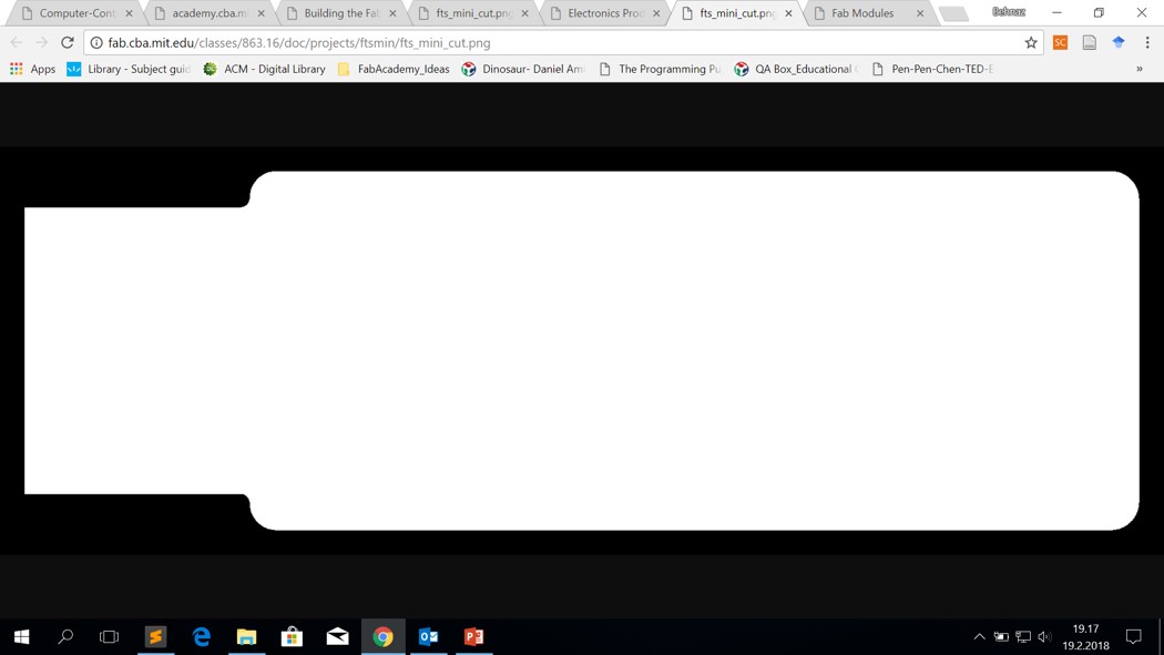
- Download the PNG files for the traces. I used this one
- Open fabmodules.org
- Input format: image (.png)
- Output format: Ronald mill (.rml)
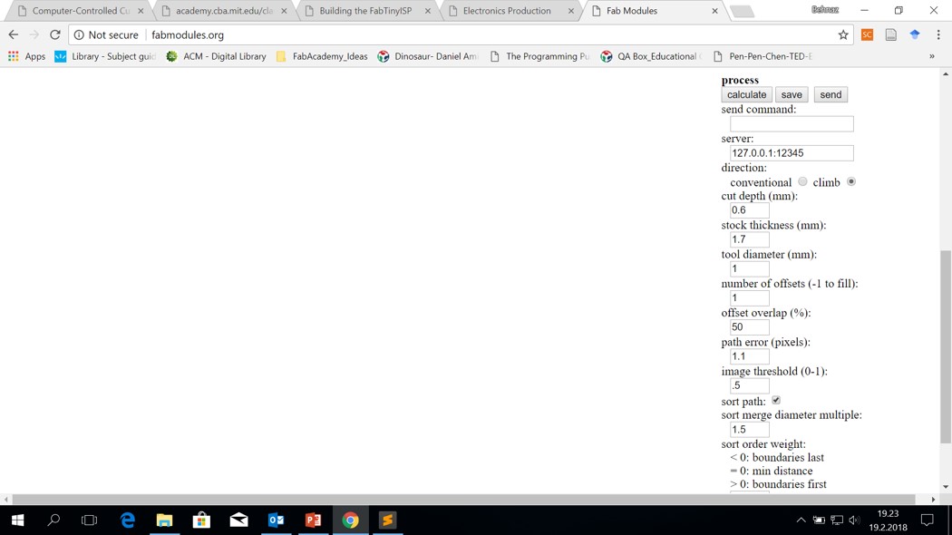
The same setting as the image of the traces. - Process: PCB outline (1/32)
The settings for Process:
cut depth: 0.6mm
- Press 'calculate' under the Process
- Hit save button under the process to save the result.
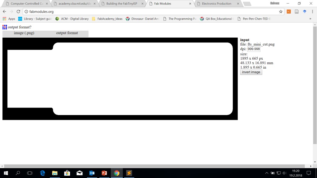
tool diameter: 1mm
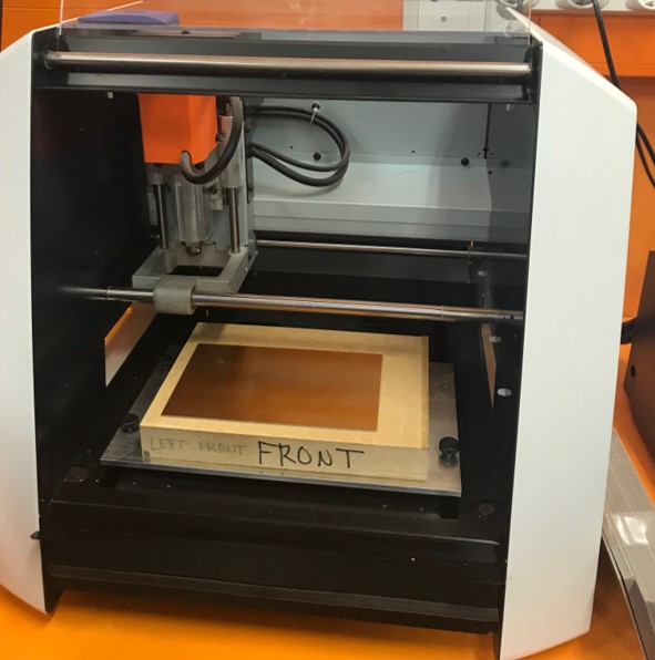
Milling Machine Setting AND Milling The PCB
- Press on button, which is on the top of the machine.
- VPanel for SRM-20 (the program)
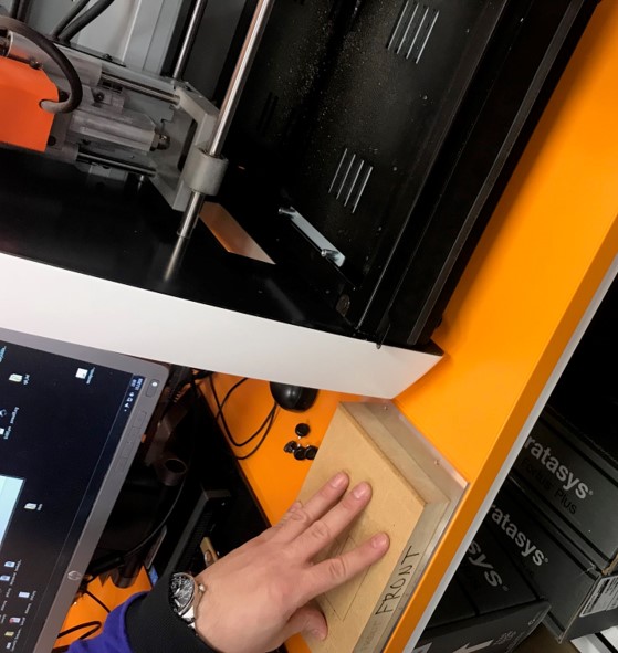
- Put a blank PCB in it. (It is light sensitive coating)
- Remove the cover from it.
- Remove 4 screws and take the plane out.
- Make sure that both PCB and plane are clean.
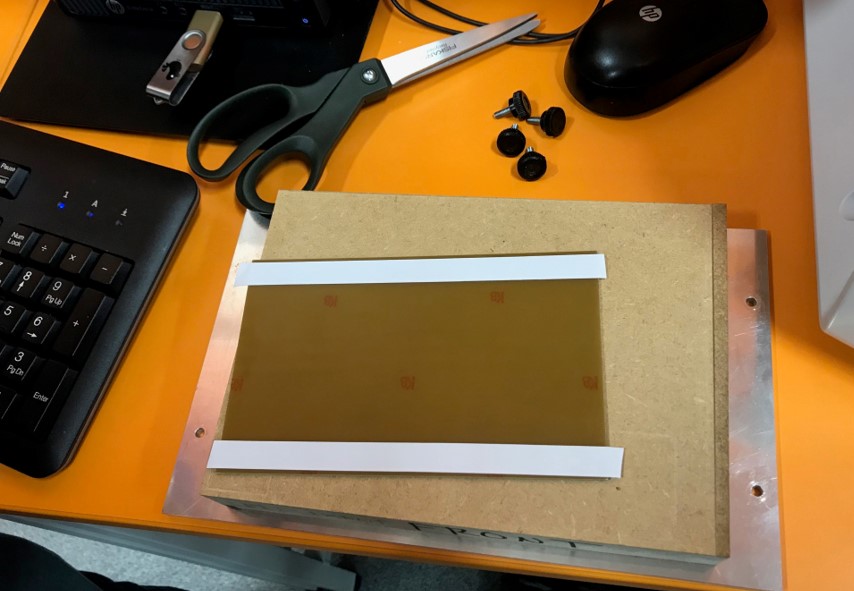
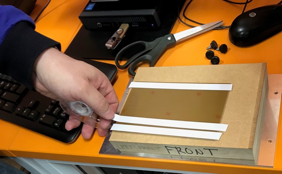
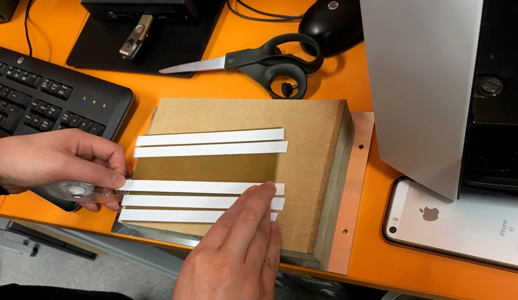
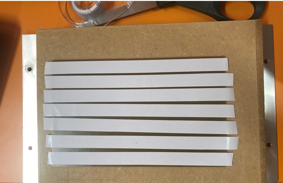
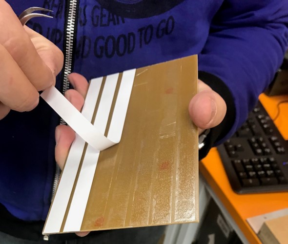
- Make layers of 2-sided tape on the PCB surface.¨Start taping from edges. And there can be a couple of milimeters between the tapes.
- Cut the extra parts of the tape out.
- Remove the papers from the tape.
- Then stick it to the plane.
- Put it from the front side into the machine.
- Tighten the screws.
- Close the door.
- Move to the view position.
- Put the mill bit inside.
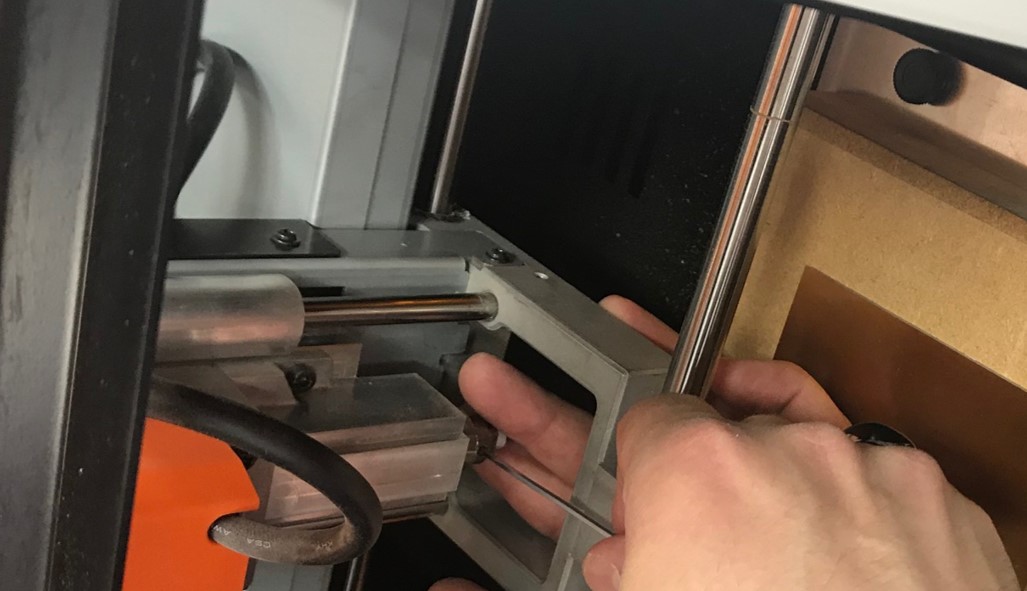
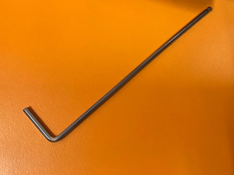
- Use the tool (allen screw) to tighten the mill bit.
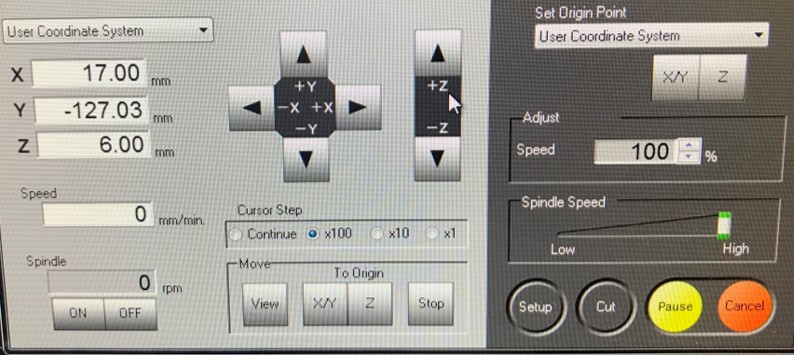
- Use +x, -x, +y, -y: for moving the head and the table to place the milling bit in a desired position.
- When it is in a place that you want, press X/Y button in the top right of the program under the 'set origin point' to set the origin point.
- Now use +z, -z: to bring the milling bit close to the PCB surface.
x100, x10, x1: under the cursor step are for different speeds. And it is better to use for example x1, when the mill bit is so close to the surface. Because it could easily break if it hits with a high speed to the surface. - When the milling bit is close enough to the surface of the plane, keep it with one hand and use the other hand to loose the milling bit using allen tool. And then slowly let it touch the surface. Then tighten it again.
- Now it is time to set Z origin by pressing Z button.
- When the z origin is set, move the bit a little bit up using +z.
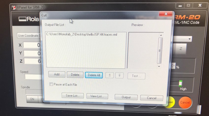
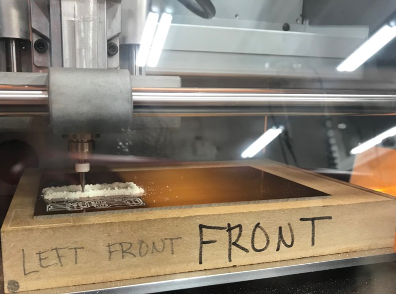
- Now it is time to load .rml file for traces. Press 'Cut' button. Then delete everything that is in the output file list. And then Add the file that you have already made ready for traces. And the press 'output' button.
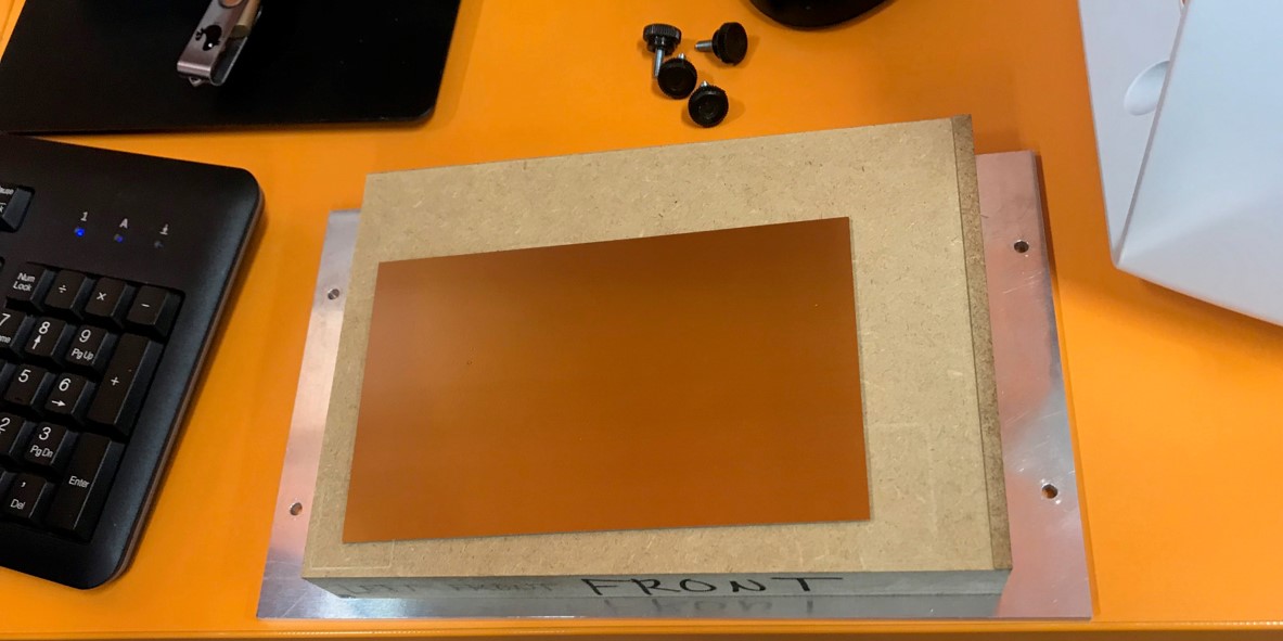
- This is the result. Also from the amount of dust that was produced while milling, we could know that the depth of cutting is good enough.
- Now it is time to change the milling bit and cut the border. We should do the same process as we did for milling the traces. But it is very important that at this stage, we do not change the origin of x and y. We just reset the origin of z.
- When the milling of the board is also done, it is time to remove dusts with a vacuum cleaner.
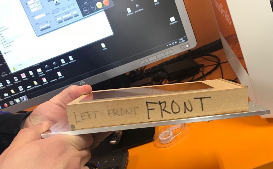
- Then remove your piece from the blank PCB.
Here one of our classmates opened the plane and then removed her piece. And this affected the cutting depth of the next millings. So it is better to remove your piece, while the plane is inside the milling machine. - Now it is time to scrub the surface of the PCB.
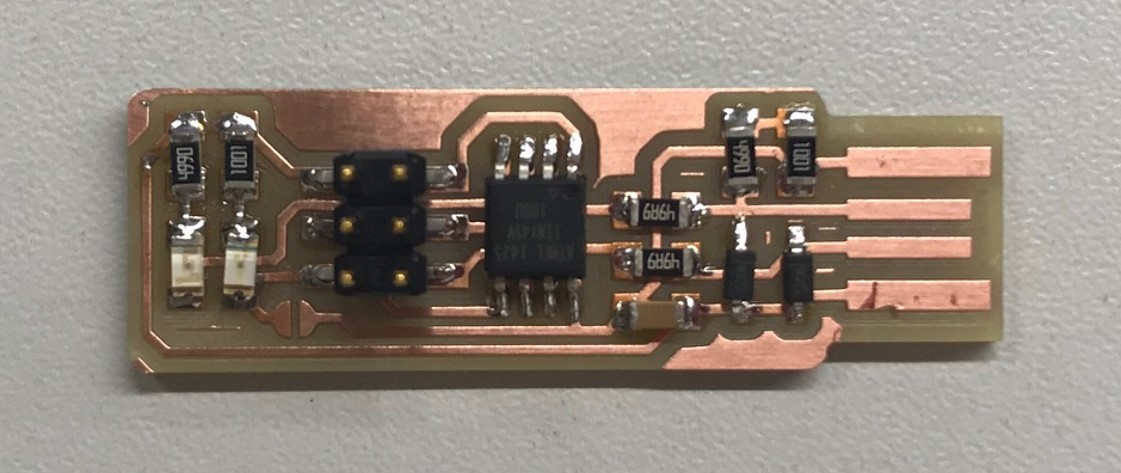
Assembling The PCB
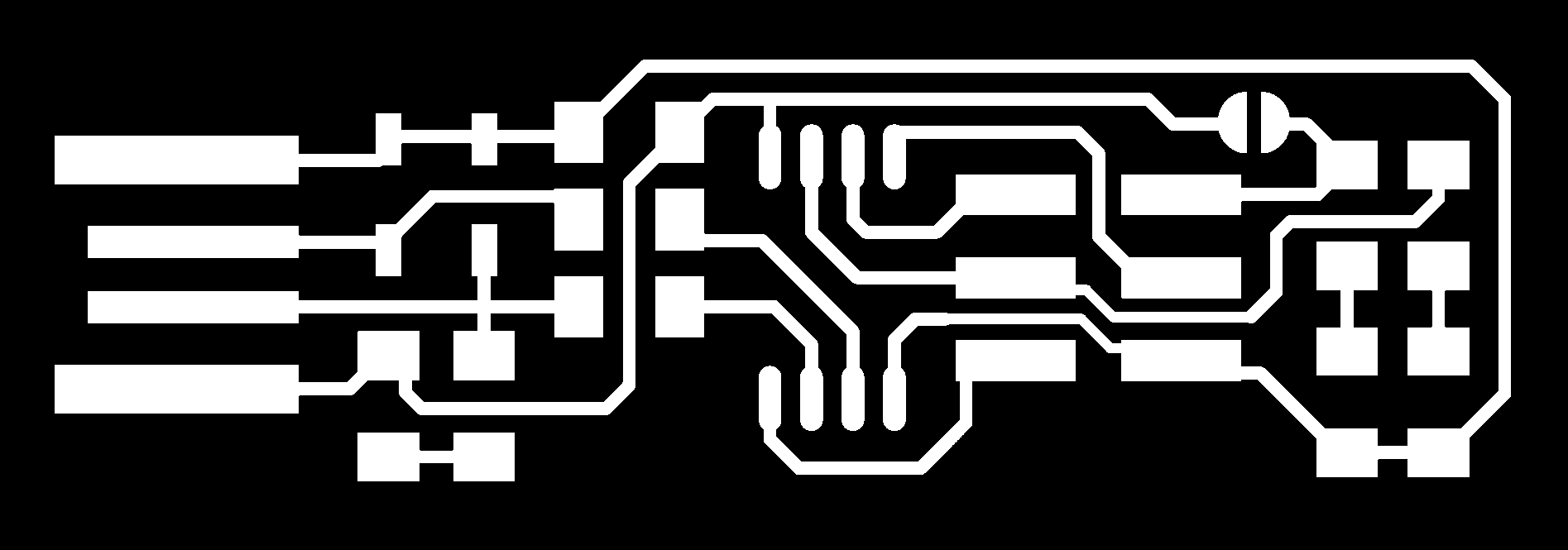
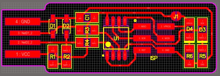
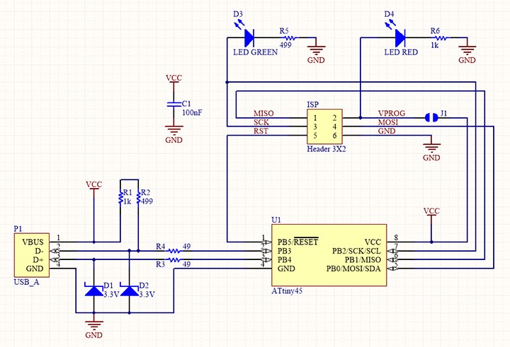
- I assembeled the PBC using Brian's chematic S and board image:
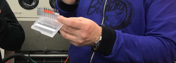
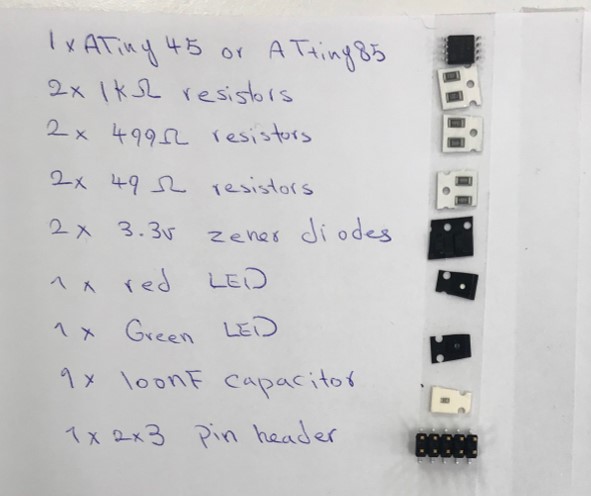
- First I collected all the components. To make it easy, Jari suggested us to write the list of components and stick 2 sided tape in front of it and place components on the tape. It was a very good way :-)
- As suggested in Brian's document, I started by soldering ATtiny45 and I did the larger items at the end in order to avoid them blocking my way and limitting my movements.
- It was so important to always check the document precisely. Because on some components there are some very tiny lines or holes on one side and it is important in which direction you place them.
- Please check Brian's Documentations if you need more details on how to solder the items on this PCB board. Because I exactly did the same.
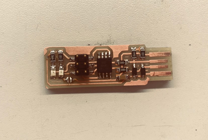
- And here is the result :-)
After Assembling The PCB
- I used a few layers of tape at the back of my PCB to make it fit properly in USB connector.
- I followed Jari and Brian's instruction for software installation, getting and building the firmware, programming the ATtiny45, testing the USB functionality and blowing the reset fuse.
- I ckecked my board visually to make sure everything is ok especially that the components are flat on the board.
- I used a multimeter to check for shorts between VCC and GND
- I installed necessary softwares:
- Git
- Atmel GNU Toolchain
- GNU Make
- avrdude
- I downloaded the firmware source code and extracted the zip file. Then Git Bashed inside the folder. And then run make command. Running this command resulted in building a file named fts_firmware.hex.
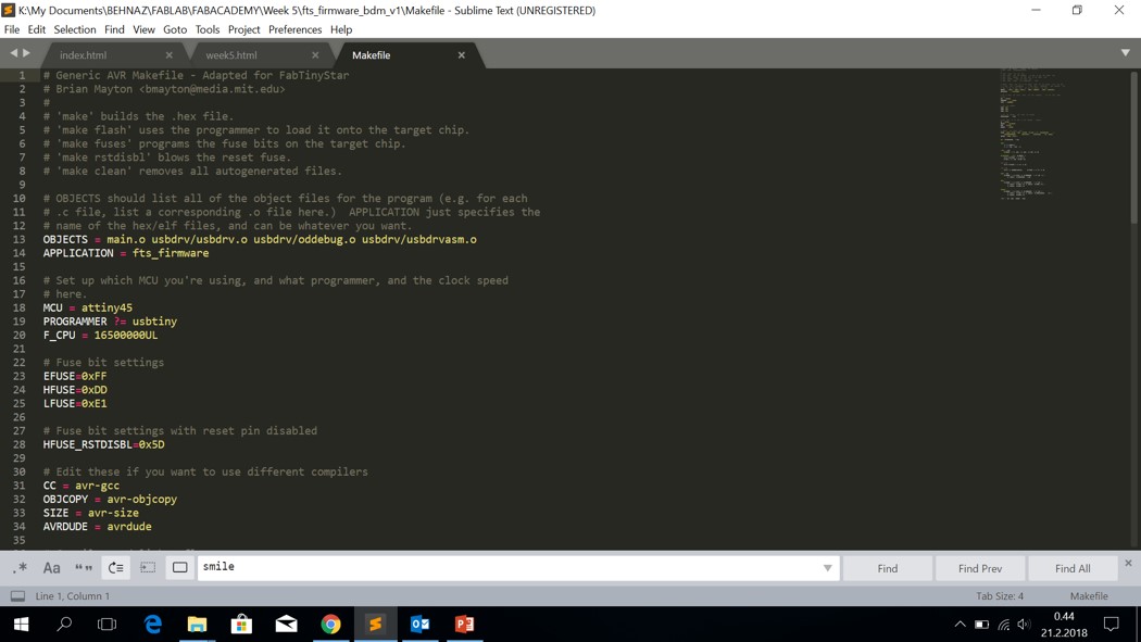
- I opened Makefile (which is in fts_firmware_bdm_v1 folder) with sublime to make sure that the default programmer is defined correct, otherwise I needed to edit it. In this case, it was defined PROGRAMMER ?= usbtiny by default, which was OK and I did not need to edit it.
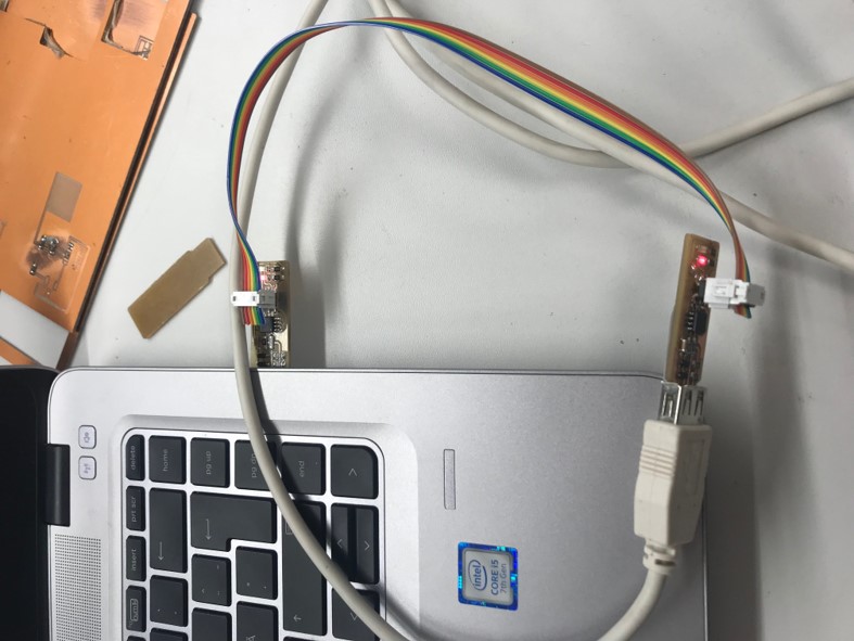
- Then I connected the programmer to the ISP header on my board and plugged them into the USB connector as you see in the picture: (the red LED also lights up)
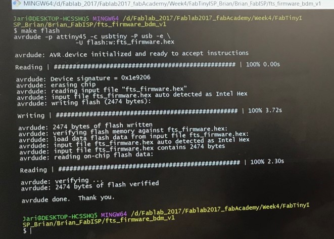
- Then by running make flash command, the target chip was erased, and programed its flash memory with the contents of the .hex file I built before.
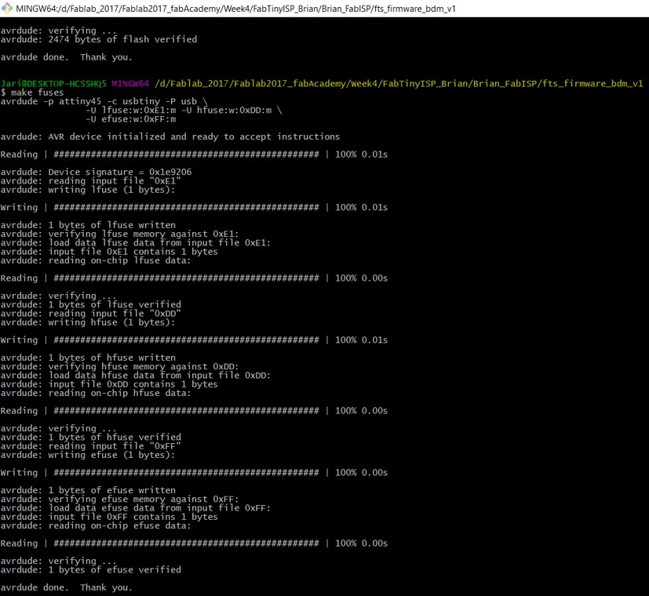
- And now it is time to set the configuration fuses. By running make fuse command, I intended to set all the fuses up except the fuse that disables the reset pin. Because this fuse should be set after making sure that USB works properly.
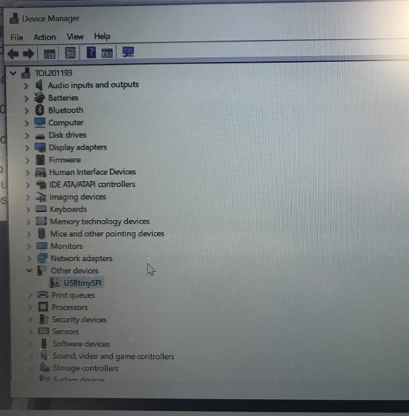
- Then I tested the USB functionality by following this path: Start → Control Panel → System → Device Manager and made sure that USBtiny device shows up here.
- Fortunately everything is working fine :-) And I can do the setting for the fuse that disables the reset pin. This setting enables us to program other boards with this chip and also disables us to program this chip again.
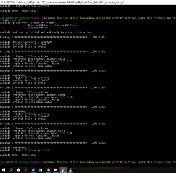
- So I connected the ISP programmer to my board and the I run this command: make rstdisbl. By running this command, I set up all the fuses including the one that disables the reset pin.
- Now it is time to destroy the bridge on the jumper that I created by solder in the soldering stage. In order to turn the board into the programmer, the connection between VCC and Vprog should be removed.
Original Design Files
RML File for Traces of the USBRML File for Outline of the USB