Group assignment
Individual assignment
Learning outcomes:
Have you:
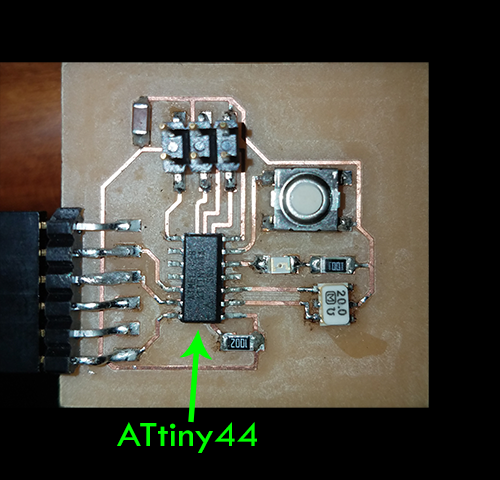
Before starting to program the board you need some knownledge of the components and microprocessor (ATtiny44) you're using and you should read the datasheets to start to understand them. One of the most important things to know abut the microprocessors are what pins do what, and where you connect the components that you are working with.
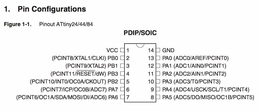
Pin 1: VCC. This is the power applied to the pin. Typically 5 volts DC. This pin has only one function. Red wire from power supply paths to here.
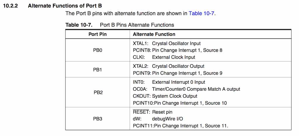
Pin 2: PB0 - PORTB-0 can be connected to an external clock, crystal oscillator input, pin change interrupt, external clock input
Pin 3: PB1 - PORTB-1 can be used for pin change interrupt, crystal oscillator output
Pin 4: PB3 - PORTB-3 can be used for RESET
Pin 5: PB2 - PORTB-2 can be used for an interrupt, clock out, pin change interrupt.
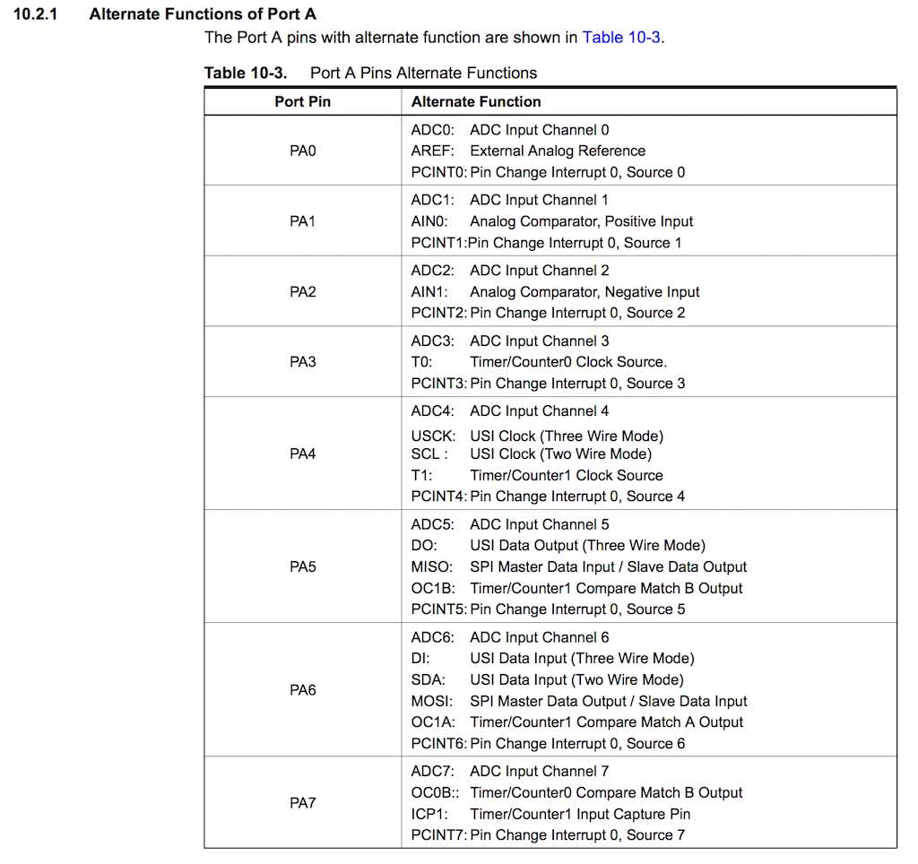
Pin 6: PA2 - PORTA-2 can be used for analog digital converter input
Pin 7: PA6 - PORTA-6 can be used for 3-wire or 2-wire communication input
Pin 8: PA5 - PORTA-5 can be used for three-wire communication output
Pin 9: PA4 - PORTA-4 can be used for analog digital converter input
Pin 10: PA3 - PORTA-3 can be used for analog digital converter input, or timer/counter, or interrupt
Pin 11: PA2 - PORTA-2 can be used for interrupt, analog digital converter input
Pin 12: PA1 - PORTA-1 can be used for interrupt, analog digital converter input
Pin 13: PA0 - PORTA-0 can be used for interrupt, analog digital converter input, and external analog reference
Pin 14: GND - GROUND - 0 volts. Black wire from power supply goes here.
Identical to the ATtiny24 except:
Identical to the ATtiny24 except:
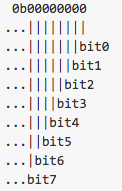
ATtiny family is a series of 8-bit microcontrollers. This means that all the information has to be divided into 8 possible blocks called bits.
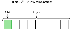
The numeration of the bits in a byte starts from the left. Is important to know that for when you want to modify the registers or send the information.
<< 2 indicates that you are moving the '1' two positions to the left and insetring 0's (like making 1.0 into 100.0)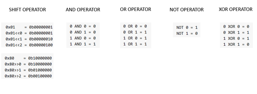
You need to know what port you are going to modify and to create the mask that will be the 'function' that will change your value as desired.
Example:
You want to put a 0 in the 4th bit slot. To do this, you create a Mask that has the shift operator, indicating the 4 positions you want to move. Then, you invert the mask and you apply the and operator. The resulting value will be the one you were looking for, same bits as the initial one but with a 0 in the 4th position.
I used this as a great reference to figuring out different aspects of this week's assignment
Each port pin consists of three register bits: DDxn, PORTxn, and PINxn. As shown in “Register Description” on page 66, the DDxn bits are accessed at the DDRx I/O address, the_PORTxn bits at the PORTx I/O address, and the PINxn bits at the PINx I/O address.
The DDxn bit in the DDRx Register selects the direction of this pin. If DDxn is written logic one, Pxn is configured as an output pin. If DDxn is written logic zero, Pxn is configured as an input pin. If PORTxn is written logic one when the pin is configured as an input pin, the pull-up resistor is activated. To switch the pull-up resistor off, PORTxn has to be written logic zero or the pin has to be configured as an output pin.
The port pins are tri-stated when reset condition becomes active, even if no clocks are running. If PORTxn is written logic one when the pin is configured as an output pin, the port pin is driven high (one). If PORTxn is written logic zero when the pin is configured as an output pin, the port pin is driven low (zero).
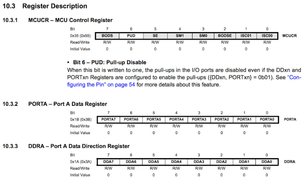
Writing a logic one to PINxn toggles the value of PORTxn, independent on the value of DDRxn. Note that the SBI instruction can be used to toggle one single bit in a port.
.jpg)
There are 3 bytes of permanent storage in the chip called 'fuse low byte', 'fuse high byte' and 'fuse extended byte'. These bytes are called fuses and can be reprogrammed as many times as you want and determines the behaviour of the chip. To do that, their value is not erased when the chip is powered off or reprogrammed.
Each microchip has its own definition for the values that must have the fuses. In this tutorial, we are going to work with the fuses of the Atmel Attiny44A.
| Name | Description | Default Value | Byte | Bit range | Datasheet page |
|---|---|---|---|---|---|
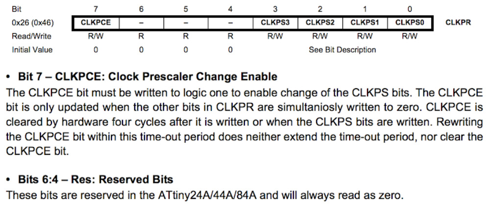
| CKDIV8 | The prescaler feature can be used to change the power consumption when not high performance is required. This feature can be used with any clock source. The prescaler divides the clock frecuency by a defined factor that can be configured using the CLKPS(3...0) register (Datasheet - Table 6-11), being its default value "0011" (divistion factor of 8). | 0 | LOW | (7) | 30 |
| CKOUT | This fuse allows us to use the chip clock as a clock source to drive other circuits. Once this bit is programmed, the PIN B2 will output the clock. | 1 | LOW | (6) | 30 |
| SUT | This fuses determine the Start-up Times for the external clock selection. This time must be long enough to ensure that the MCU is kept in reset mode while the clock is changing (is not stable). Its default value defines the longest Start-up time. | 10 | LOW | (5,4) | 26 |
| CKSEL | The AMTEL Attiny44A can use several clock sources. By default, the clock used is the internal 8MHz oscillator. The available configurations can be found in the datasheet, in table 6-1. | 0010 | LOW | (3...0) | 25 |
| RSTDISBL | When programmed (0), the PB3, instead of being used as a reset pin, it can be used as an I/O pin. | 1 | HIGH | (7) | 3 |
| DWEN | This fuse allows the activation of the 'debug' mode. Once it is programmed, the RESET port is configured as a bidirectional I/O pin with pull-up enabled. | 1 | HIGH | (6) | 150 |
| SPIEN | Fuse that enables serial program and data downloading. Once unprogrammed this fuse, in order to reset its value, you will need a 12V programmer. | 0 | HIGH | (5) | 159 |
| WDTON | A watchdog timer is a mechanism to prevent closed loops and errors in the microchip. It consists on a decreasing counter. If it reaches 0, it generates a timeout signal that triggers an action to restore the system. To avoid this, the program must restart the timer before it times out. | 1 | HIGH | bit range | 41 |
| EESAVE | If programmed (0) the EEPROM memory will be preserved through chip erase. | 1 | HIGH | (4) | 159 |
| BODLEVEL | This fuse controles the Brown-out detector. A Broun-out detector is a circuit that monitors the supply voltage while operating. It compares the supplied voltage to a fixed one. If the supplied voltage decreases blow a fixed one (VBOT-), the Brown-out reset is enabled until the voltage raises above a VBOT+. Then a timer starts; if it times out, the reset is disabled. By default, the Brown-out detector is disabled. In table 20-6 of the Datasheet all the modes are specified. | 111 | HIGH | (2...0) | 159 & 176 |
| SELDPRGEN | This fuse, if programmed, allows to the device the ability to upload a program to the MCU by itself. | 1 | EXTENDED | (0) | 152 |
[As seen, there is just one bit in the Extended byte of the fuses whose value will change the microchip behaviour. The bytes 7...1 should be set with a value of 1.]
CKDIV8 is a prescaler feature to lower the microcontroller clock.
The prescaler feature can be used to change the power consumption when not high performance is required, or to ensure the performance (and programability) at any legal VCC. This feature can be used with any clock source. The prescaler divides the clock frecuency by a defined division factor that can be configured using the CLKPS(3:0) register (Datasheet - Table 6-11), being its default value “0011” (divistion factor of 8).
When CKDIV8 is unprogrammed, CLKPS bits will be reset to “0000”. If CKDIV8 is programmed, CLKPS bits are reset to “0011”, giving a division factor of eight at start up.
****The device is shipped with the CKDIV8 Fuse programmed****
.jpg)
Working in the Arduino Program, the first things we need to do are setting the parameters we are writing in to match the components that we have on our board.
.png)
.png)
.png)
.png)
Making the board say hello via Morse Code seems like the obvious thing to make the "Hello World" board do. So lets check out some Morse Code to see what we need to program:

According to the chart, we need to make sure the delay's of the longer "blinks" are x3 as long as the shorter "blinks". I am also going to have a nice long pause in between each letter for clairty's sake.
Here is the Final Code
.png)