Assignment 5: Electronics Production
Make an in-circuit programmer by milling the PCB, then optionally trying other processes
Learning outcomes:
-
Describe the process of milling, stuffing, de-bugging and programming
-
Demonstrate correct workflows and identify areas for improvement if required
Group assignment:
-
Characterize the design rules for your in-house PCB production process: document feeds, speeds, plunge rate, depth of cut (traces and outline) and tooling.
-
Document your work (in a group or individually).
-
Document your work to the group work page and reflect on your individual page what you learned.
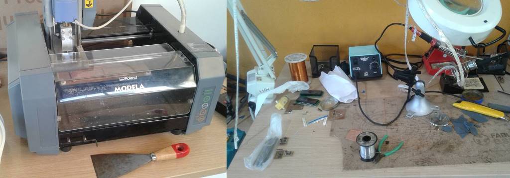
For this assignment we used the Roland Modela MDX 20 machine. This machine has the following technical specifications:
Size table: 220 mm x 160 mm
Size operation area: 203 mm x 152 mm
Maximum resolution: 0.00625 mm/step
Size operation area: 203 mm x 152 mm
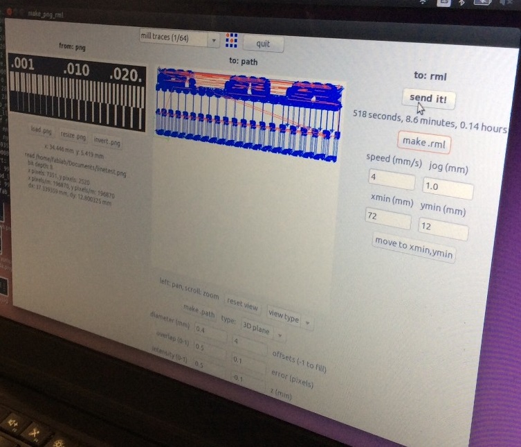
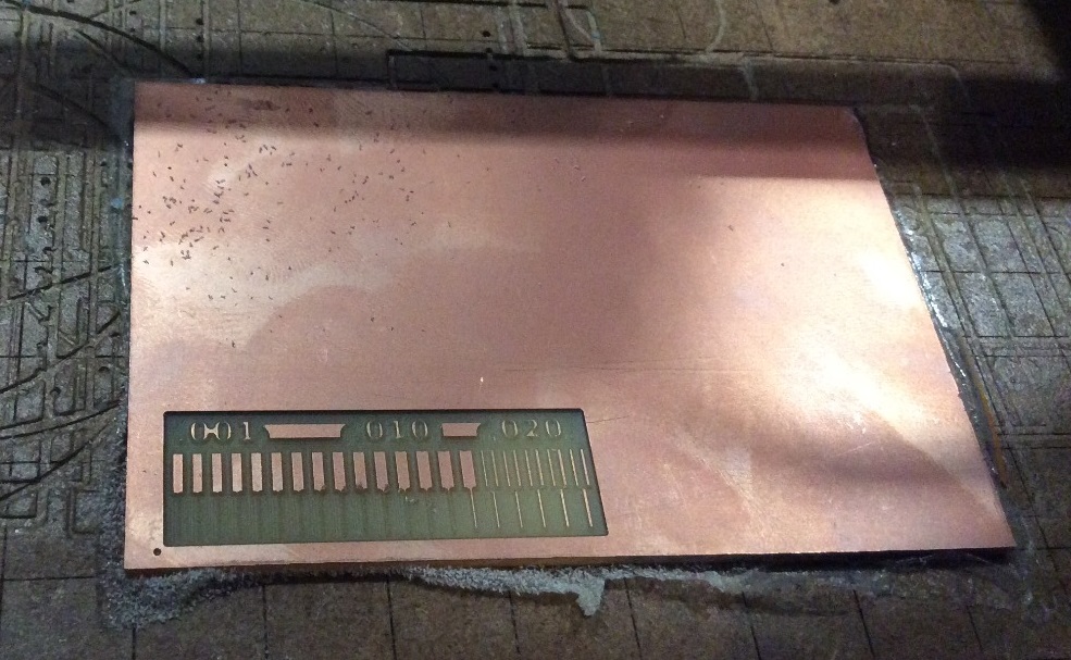
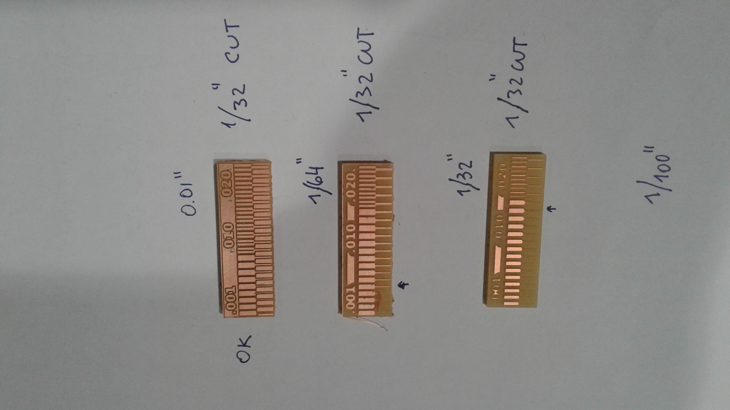
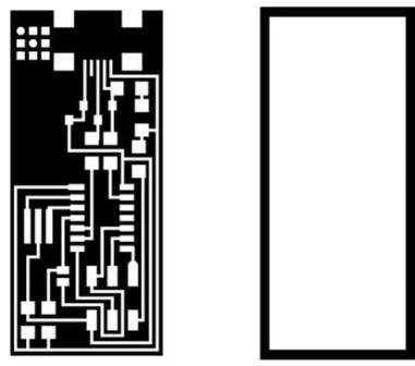
To characterize the design rules, we used an image that we got from the fabacademy webpage. It will be used to set the parameters that should be used while milling our boards. The image can be found at: https://academy.cba.mit.edu/classes/electronics_production/linetest.png
The design features different sizes on the lines. These different sizes must be analyzed and evaluated in order to find the correct measurements or parameters for milling the boards.

The design features different sizes on the lines. These different sizes must be analyzed and evaluated in order to find the correct measurements or parameters for milling the boards.
Making this assignment turned out to be a great challenge for me. I had never worked before with electronics-related subjects before. I had to ask my colleagues and my advisors for help to help me with this new challenge.
Making this assignment turned out to be a great challenge for me. I had never worked before with electronics-related subjects before. I had to ask my colleagues and my advisors for help to help me with this new challenge.
Making this assignment turned out to be a great challenge for me. I had never worked before with electronics-related subjects before. I had to ask my colleagues and my advisors for help to help me with this new challenge.
Making this assignment turned out to be a great challenge for me. I had never worked before with electronics-related subjects before. I had to ask my colleagues and my advisors for help to help me with this new challenge.
Individual assignment:
-
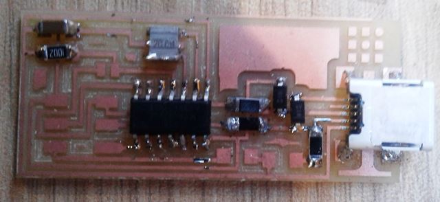
Make an in-circuit programmer that includes a microcontroller by milling and stuffing the PCB, test it to verify that it works.
Making this assignment turned out to be a great challenge for me. I had never worked before with electronics-related subjects before. I had to ask my colleagues and my advisors for help to help me with this new challenge.
Step 1: The first step for this assignment was to receive brief advice on the basics of electronics, electronic cards and the use of equipment to mill and solder the components of an electronic card.
Step 2: Then I download the files for the inside and the outside of the board from the web of the assignment:
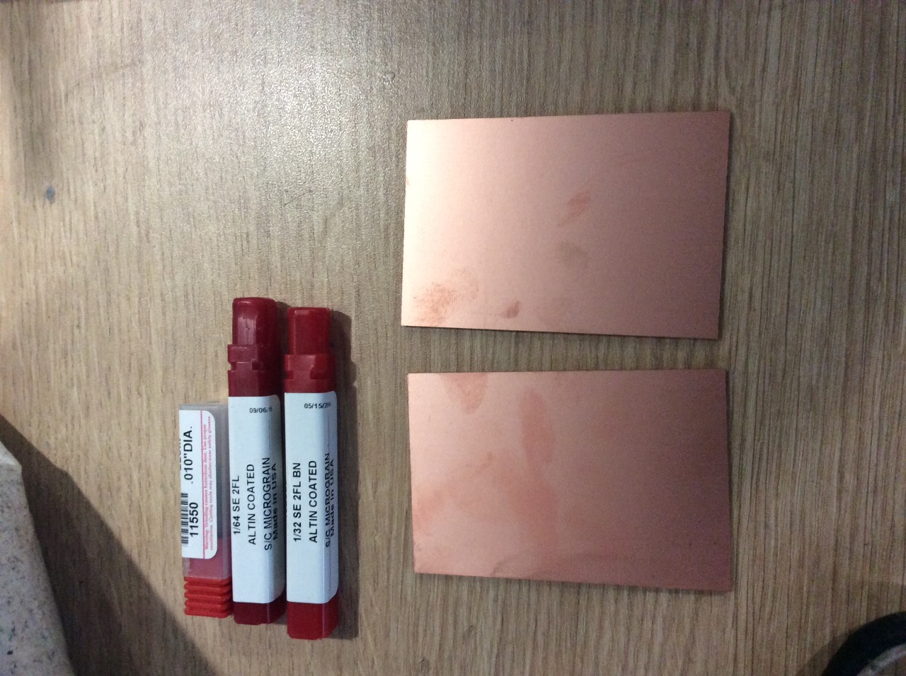
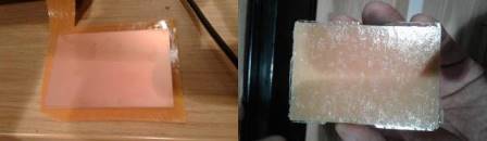
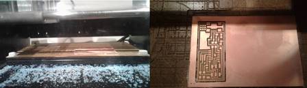
Step 3: Then cut a piece of 2x3-inch PCB bakelite plate. Then I put a glue paper so that the cut of the plate does not move from the work table:
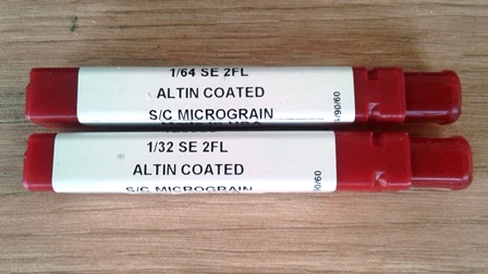
The 1/64 cutter was used for the inner cut and the 1/32 cutter was used for the outer cut:
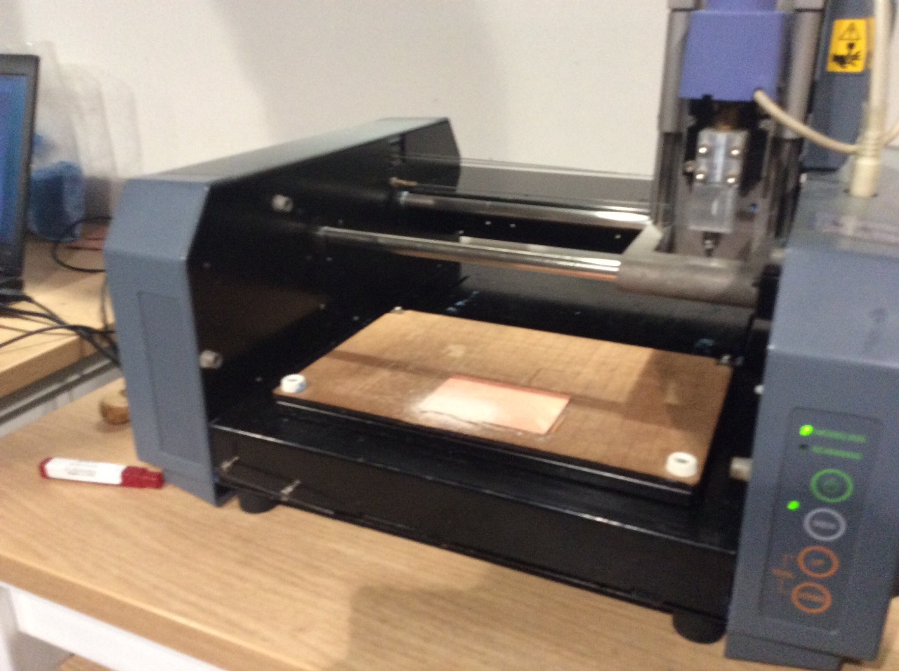
Step 4: Next, the Roland Modela 3D Plotter MDX-20 milling machine was prepared. Then the Modela program was configured for the inner cut and for the outer cut.
Milling process:
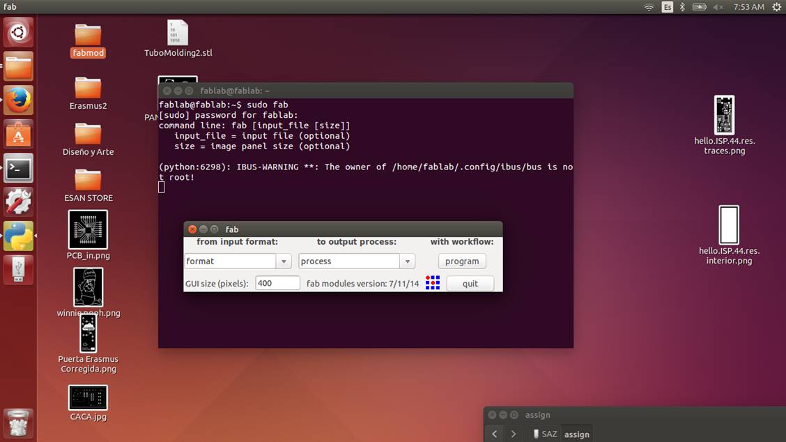
a. Open the milling program with the "sudo fab" command.
b. Select the file with the strokes for the engraving of the tracks.
c. Choose "mill traces (1/64)" for the recording of the tracks.
d. Choose the tolerance parameter: 0.1 error (pixels).
e. Before starting the milling, the height must be calibrated, for this press the view button so that the milling cutter is positioned in position 0,0.
f. Then in the software enter the X and Y coordinates and press the "move to Xmin, Ymin" button and very carefully use the "up" and "down" buttons to bring the bit closer to the surface.
g. Click on the button "Send it!"
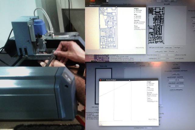
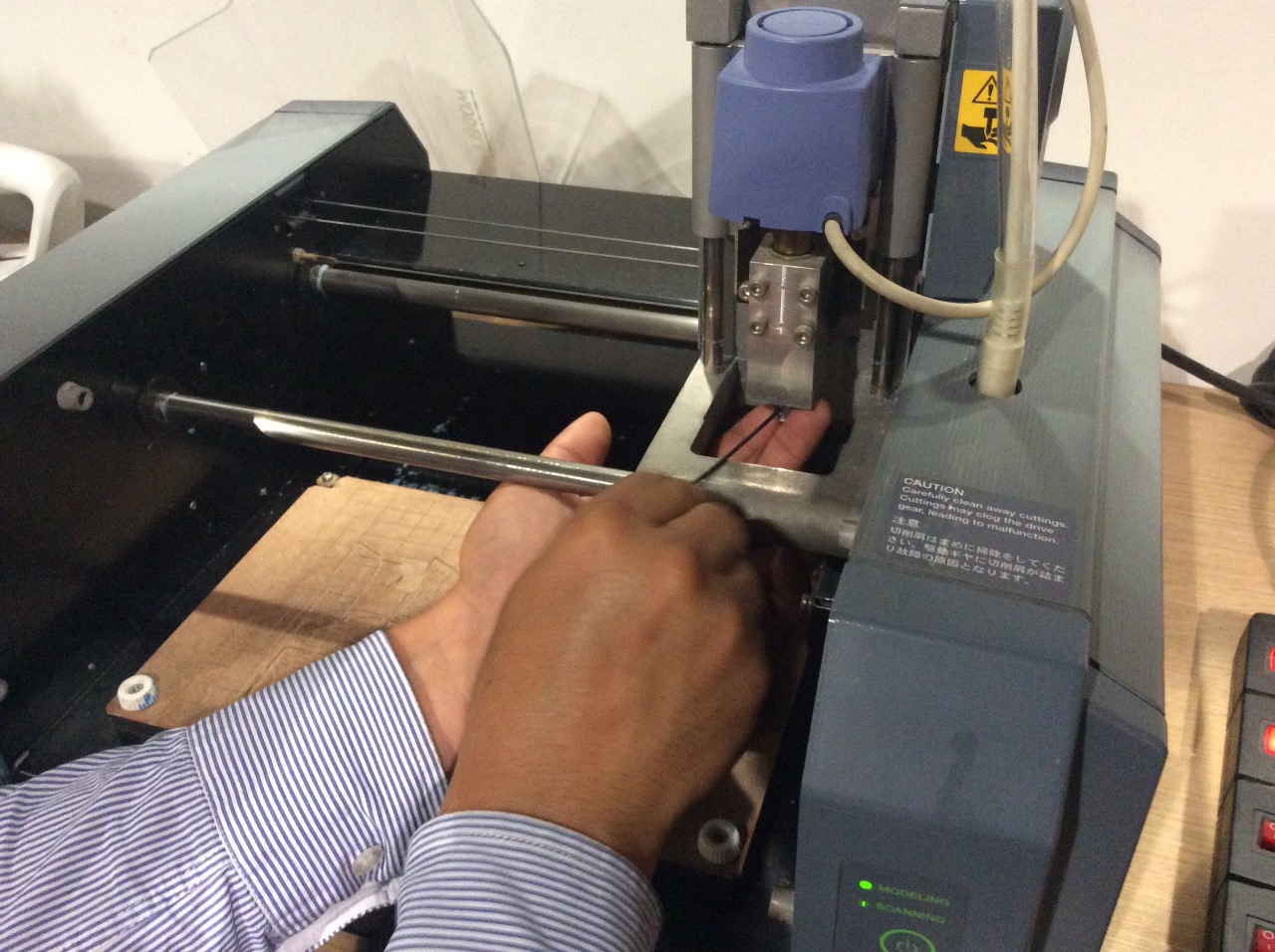
Step 5: I was watching the cutting process with the hope that the configuration was correctly done. If the cutting configuration is not carried out correctly, it is necessary to repeat the whole process. At the end of the cuts I proceeded to clean the remains with an air vacuum:
Step 6: The next step was to request the components of the PCB in the Fab Lab ESAN warehouse. The components were requested according to the diagram of the PCB posted on the website of the Fab Academy
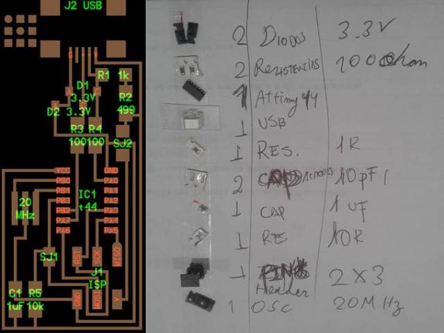
Step 7: The next step was to solder each component of the PCB one by one. This was a slow and prolonged process, it was necessary to have a lot of patience. Sometimes I was about to burn myself with the welding gun, other times I had trouble locating the components in the correct place on the PCB:
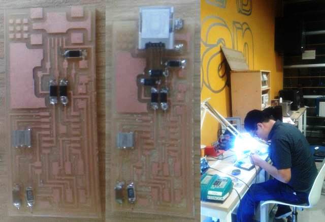
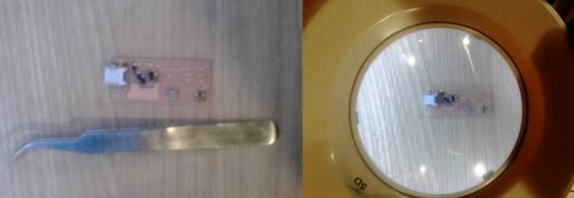
It was necessary to use a clamp and a magnifying lens due to the small size of the components. I needed about three hours to finish welding all the components of the card:
It was a new experience for me. I believe that little by little I will be improving my skills for the cut and the soldier of a PCB:
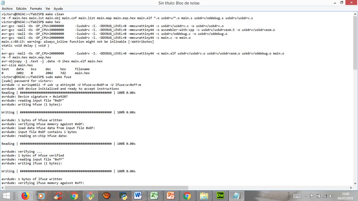
Step 8: The next step was to program the PCB.
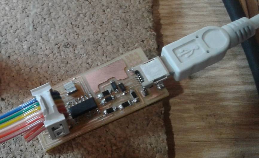
To program the PCB I used the following commands:
victorv@ENIAC:~/fabISP$ make clean
victorv@ENIAC:~/fabISP$ make hex
victorv@ENIAC:~/fabISP$ sudo make fuse
victorv@ENIAC:~/fabISP$ sudo make program
victorv@ENIAC:~/fabISP$ lsusb